You are currently viewing SemiWiki as a guest which gives you limited access to the site. To view blog comments and experience other SemiWiki features you must be a registered member. Registration is fast, simple, and absolutely free so please,
join our community today!
            WP_Term Object
(
    [term_id] => 24
    [name] => TSMC
    [slug] => tsmc
    [term_group] => 0
    [term_taxonomy_id] => 24
    [taxonomy] => category
    [description] =>
    [parent] => 158
    [count] => 585
    [filter] => raw
    [cat_ID] => 24
    [category_count] => 585
    [category_description] =>
    [cat_name] => TSMC
    [category_nicename] => tsmc
    [category_parent] => 158
    [is_post] =>
)

WP_Term Object
(
    [term_id] => 24
    [name] => TSMC
    [slug] => tsmc
    [term_group] => 0
    [term_taxonomy_id] => 24
    [taxonomy] => category
    [description] =>
    [parent] => 158
    [count] => 585
    [filter] => raw
    [cat_ID] => 24
    [category_count] => 585
    [category_description] =>
    [cat_name] => TSMC
    [category_nicename] => tsmc
    [category_parent] => 158
    [is_post] =>
)
I’m looking forward to the 2013 TSMC Open Innovation Platform Ecosystem Forum to be held Oct. 1[SUP]st[/SUP] in San Jose. One paper in particular that has my attention is titled, “An Efficient and Accurate Sign-Off Simulation Methodology for High-Performance CMOS Image Sensors,” by Berkeley Design Automation & … Read More
At TSMC’s OIP on October 1st, Mentor Graphics have 5 different presentations. Collect the whole set!
11am, EDA track. Design Reliability with Calibre Smartfill and PERC. Muni Mohan of Broadcom and Jeff Wilson of Mentor. New methodologies were invented for 28nm for smart fill meeting DFM requirements (and at 20nm me may … Read More
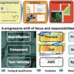
Increasingly, end users in some markets are requiring soft error rate (SER) data. This is a measure of how resistant the design (library, chip, system) is to single event effects (SEE). These manifest themselves as SEU (upset), SET (transient), SEL (latch-up), SEFI (functional interrupt).
There are two main sources that cause… Read More
Almost without exception these days, semiconductor products face strict power and thermal budgets. Of course there are many issues with dynamic power but one big area that has been getting increasingly problematic is static power. For various technical reasons we can no longer reduce the voltage as much as we would like from one… Read More
The history of TSMC and its Open Innovation Platform (OIP) is, like almost everything in semiconductors, driven by the economics of semiconductor manufacturing. Of course ICs started 50 years ago at Fairchild (very close to where Google is headquartered today, these things go in circles). The planarization approach, whereby… Read More
The TSMC Open Innovation Platform® (OIP) Ecosystem Forum brings TSMC’s design ecosystem member companies together to share with our customers real-case solutions for customers’ design challenges and success stories of best practice in TSMC’s design ecosystem.
More than 90% of the attendees last year said “this… Read More
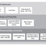
I think by now all of us know, or have heard about 20nm process node, its PPA (Power, Performance, Area) advantages and challenges (complexity of high design size and density, heterogeneity, variability, stress, lithography complexities, LDEs and so on). I’m not going to get into the details of these challenges, but will ponder… Read More
IC designers have been creating with hierarchy for years to better manage large design sizes, however for the test world the concept of hierarchy and emerging standards is a bit newer. TSMC and Synopsys jointly created a webinarthat addresses hierarchical test, so I’ve attended it this week and summarized my findings here.… Read More
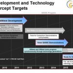
The presentations from the 450mm sessions at SEMICON West are up now. After talking to equipment manufacturers and the foundries I’m fairly confident 450mm wafers will be under our Christmas trees in 2016, absolutely. TSMC just increased CAPEX again and you can be sure 450mm is part of it. SEMI has a 450mm Central landing page HERE… Read More
There is an interesting article on Seeking Alpha, “A More Profitable Semiconductor Company Than Intel”, and for a change the author does not PRETEND to know semiconductor technology. Refreshing! Personally I think the stock market is a racket where insiders profit at the expense of the masses. But if you are going to gamble you … Read More