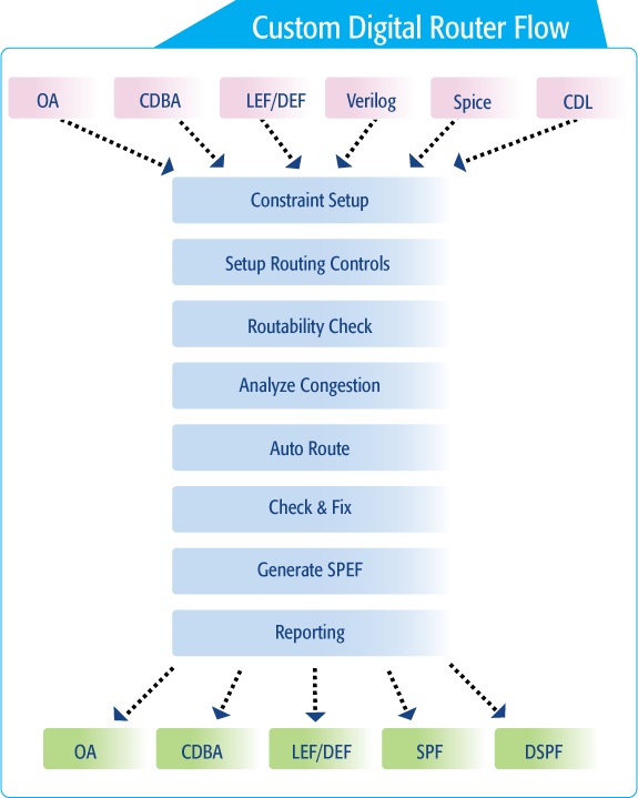
DAC2025 SemiWiki 800x100

An Affordable 3D Field Solver at DAC

An Affordable 3D Field Solver at DAC
by Daniel Payne on 06-17-2011 at 6:35 pm

Intro
Massimo Sivilotti, Ph.D of Tanner EDA showed me their 3D field solver in the HiPer PX extraction tool at DAC last week.

Notes

Tool Suites – schematics, layout, SPICE simulation, DRC/LVS
– HiPer PX: 3D Field solvero Layers, dielectrics,
o Finite element analysis
o Boundary element methods
o 2D mode for pattern matching
o PDK – includes the info for PX extraction
o 3D viewer to see the IC Layout
o Offered for a few years now
o Extract: Devices, parasitic, interconnect
o Produces RC netlist (not L, not s-parameters), coupled C
o Take parasitic from PX extraction then view it in Schematic editor (S-Edit)
 Swap out cell parasitics by changing the view
o Run times are more limited by your simulator, not the extraction
o Built-in netlist reduction algorithms (supply a frequency range), typically the reduced netlist is 10% the size of the original netlist
o Not a multi-core algorithm yet (T-Spice is multi-core for circuit simulation)
o Developed at TU Delft in Europe, licensed technology
o Runs on both PC and Linux (32 or 64bit)
o Comparable accuracy with Assura RX

Licensing – Sentinel
– Dongles
– Commuter
– Time-based
– Rentals
– Even permanent licenses

L-Edit – used for stacked die layout with IC and Mems
– Packaging techniques to locate all pads

3D Solid Modeler
– Used for MEMS Design – have a solid modeler (air or dielectrics)
– Interfaces to Finite Element Analysis
– Optical example with mirror

Summary
Tanner EDA continues to offer affordable IC design tools, HiPer PX offers both 3D and 2.5D extraction depending on the accuracy that you need.


Hardware Configuration Management at DAC

Hardware Configuration Management at DAC
by Daniel Payne on 06-17-2011 at 6:20 pm

Intro
Show me what has changed in my RTL or Schematic since the last time I looked. This task is now automated by Cliosoft with their new hierarchical tool called Visual Design Difference (VDD). Srinath showed me what was new for DAC.


Srinath Anantharaman

Notes
LSI, STMicro – use DesignSync for their DM but use VDD for seeing visual differences.

Visual Diff – Tool introduced just over one year.
– This year it handles hierarchy.
– Can also ignore Cosmetic Changes that have no electrical changes.
– If you make changes to your RTL design, then how do you see what has changed?
– Demo: Compared two versions of a designo Tree widget shows the hierarchy of where to find the changes
o Expand the tree widget, see each difference in logic
o See changes in different colors
o Zoom on changes per pin or net, complete text description
o Standard feature at no extra cost for existing customers
o Can even see property changes along with logical changes

Clients: Virage – started with Springsoft Laker, then Virtuoso, now Custom Designer (stayed with Cliosoft DM throughout)

Summary
If your IC design team has two or more engineers then your job will be made easier with a tool like VDD from Cliosoft.

Also Read

Cadence Virtuoso 6.1.5 and ClioSoft Hardware Configuration Management – Webinar Review

How Avnera uses Hardware Configuration Management with Virtuoso IC Tools

Hardware Configuration Management and why it’s different than Software Configuration Management


Circuit Simulation update from Cadence at DAC

Circuit Simulation update from Cadence at DAC
by Daniel Payne on 06-17-2011 at 6:06 pm

Intro
In the bloggers suite I met with John Pierce of Cadence last Wednesday to get an update on what’s new with circuit simulation at DAC this year.

Notes

News – market is growing, RF CMOS simulation is growing
– Show on RF (MTT – Microwave Technology ) this week, sharing a booth with AWR this week
Recent news with Lorenz (EM tool to create inductors), they’re part of Connections program
– APS RF released on year ago (Parallel in the new engine)
– RF usability improved, able to do s-parameter analysis

Virtuoso APS – continued to improve, up to 16 cores
– December 2010 now you can go distributed, across machines
– No special setup required
– Uses more tokens
– Super Threading: multi-core plus distributed processing (multi-core per box)
– Typical usage: Two machines, 4 cores per machine

UltraSim – looking at next generation technologies
– Usability and speed improvements done and planned
– New developers added
– Did a new RF model

Modeling – how to model FInFET (Tri-gate)?
– Compact Modeling group involvement

Altos – acquired library characterization company
– Integrated with them last year, especially memory characterization
– Works with either Spectre or UltraSim or internal simulator

Growth – Altos had 11 out of 20 top semi companies for library characterization
– Good collaboration over past 12 months too (Jim Mccanney)

Spectre – New in last year is APS and distributed
– Shares models with UltraSim

AMS Designer – transistor simulation plus HDL
– Real number modeling (standard part of SystemVerilog) lets you model analog effects in a logic verification environment
– Did a paper at the ARM conference last year, DVCON this year (assertions plus real number modeling)
o Help ADC test bench verification
– Adoption of real number modeling is driven by the design style more than the technology
– Work with designersguide.com on training the next generation of AMS designers, classes tailored to the client and offer consulting services
– Knowlent went out of business as Analog Verification IP (too limited of an approach, not portable)
– How to influence the next generation, Universities

Parasitic Aware Design – simulation with real parasitic, as early as possible in the flow
– Quickly go from schematic to layout to extracted parasitic, better simulation results
– Virtuoso can help manage the whole parasitic flow

IMS Chips (Germany) – Used Custom Designer, then went back to Virtuoso (Feb 2011)

Wolfson (UK) – Uses SNPS digital tools, and internal analog tools. They evaluated Custom Designer but choose Virtuoso plus digital flows.

Summary
Cadence has plenty of competitors in the circuit simulation space so they continue to update and innovate their tools to stay current. Only three vendors offer an integrated co-simulation between SPICE and a widely-adopted HDL simulator (Cadence, Mentor, Synopsys).


Reduced IC leakage at DAC

Reduced IC leakage at DAC
by Daniel Payne on 06-17-2011 at 5:46 pm

Intro
Neal Carney, VP of Marketing at Tela Innovations provided me an update at DAC last week. Their company partnered with TSMC to reduce leakage in IC designs by biasing the gate lengths on your paths that are non-critical to timing.

Notes

Why do this?
– Reduce leakage
– Increase gate lengths on paths with slack
– Recharacterize cells for change channel length, new performance
– Take the output from Primetime for paths with slack
– Our tool also has a timing engine built into it
– Fine grain optimization for leakage optimization
– Our tool does more cell swaps than other tools do
– Can swap multi vt cells as well
– TSMC has four Vt choices, but with gate biasing you have finer control than just swapping Vt
– Gate biasing doesn’t require another mask
– Optimize for: Performance, leakage, costs
– At 28nm the PowerTrim libraries should become more mainstream
– At 40nm, you can bias the gate length to optimize as well
– Another technique for 28nm is to start with 35nm then use gate biasing
– Customers can ask for design services from Tela, or ask TSMC to use PowerTrim
– Customers: LSI Logic, Melanox, undisclosed (over 50 tapeouts so far)
– Gate biasing can make the device go faster (more leakage) or slower (less leakage)

Summary
If you fab with TSMC and want to reduce your leakage currents, then consider the PowerTrim library approach.


Cadence spinout at DAC

Cadence spinout at DAC
by Daniel Payne on 06-17-2011 at 5:37 pm

Intro
I remember when Celestry was acquired by Cadence because that gave them a hierarchical Fast SPICE simulator to compete with HSIM. In 2007 part of Celestry spun out from Cadence and became Proplus, which now offers a SPICE simulator called NanoDesigner.

Notes
Proplus – US company, founded in 1995 (Used to be Celestry, acquired by Cadence, spun out in 2007)
– R&D in Beijing and Silicon Valley
– NanoDesigner (4 years old): SPICE tool, not Fast SPICEo Compete with: Spectre, FInesim, HSPICE
o Accuracy is the goals
o Statistical SPICE (Monte Carlo technique)
o Customers: Not disclosed
o Pricing: Not disclosed
– IR/EM Verificationo Partnership with Grid Simulation Tech
o Customers: Not yet
Summary
I hadn’t heard of Proplus before last week, so I’ve added it to the list of all SPICE tools on our wiki page.


RLCK reduction tool at DAC

RLCK reduction tool at DAC
by Daniel Payne on 06-17-2011 at 5:23 pm

Intro
Most EDA parasitic extraction tools have built-in RC reduction with no user control however at DAC I learned how Edxact offers a stand-along RLCK reduction tool for IC designers that want more control over what happens to their extracted netlists.


Daniel Borgraeve (on right)

Notes
Edxact
– Started seven years ago
– Fifteen people in the company
– Based in France
– Jivaro: RLCK reduction (RLCC) with user control of results
o Many algorithms to choose from
o Used by Aglient in their GoldenGate tool (RF Simulator)
o Used by Intel
o About 25 customers world wide (Asia, Japan, Korea, US)
o Part of TSMC AMS Reference flow 2.0
o Pricing starts at $100K per license per year

– Comanche:
o Read parasitic
o Create R values point to point, calculate delays
o CAD developers can compare two netlists (Golden versus some extraction tool)
o Parasitic analysis platform
o Used by: AMD, ST Ericsson
o Pricing starts at $100K per license per year
– Partners
o Altos (Library Characterization, used Jivaro)
o Cadence (Integrated into Virtuoso)
o SpringSoft (Integrated into Laker, can annotate parasitic into Laker)
o Mentor (read DSPF, Eldo formats)
o Synopsps (support Star RC and HSPICE syntax)
o TSMC – part of AMS Reference flow
– Runs on: Solaris, Linux, Mac

Summary
If you want more control while reducing RCLK netlists then consider looking at Edxact tools.


Ciranova Update at DAC

Ciranova Update at DAC
by Daniel Payne on 06-17-2011 at 4:55 pm

Intro
Ciranova offers you an alternative for analog layout automation besides Cadence Virtuoso. Mark Nadim provided me an update at DAC last Wednesday.

Notes
New in 2011
– New GUI with schematic, layout and constraints
o Cross probing between all three windows
– Schematic for constraint entry
o Can start with a blank schematic, enter new design
o Read any native OA schematic
o See all the MOS instances in a tree, define layout constraints very quickly
o Drag and drop constraints
o Cross probe between MOS list and Schematic view
o Hierarchy supported
– Helix First Look
o Schematic and Analog constraints in, layout out
o Find in netlist common bulks, get placed together
o Easy way to create initial layout constraints, does auto grouping of layout
– New customers: Marvel
– 28nm migration is important, Helix is an easier way to conform to new design rules
o Auto placement helps on minimum rules
o Read design rules for density and Helix can push transistors apart to reach the rules
– Create many alternative layouts, Extract a netlist, use Calibre parasitics, create fully extracted netlist ready for Berkeley AFS
– Users: Initially the Circuit Designer starts, then handed off to the Layout Designer for completion
– Routing Example: pattern based constraints used, then autoroute between all the rows and columns of placed Devices
– New way to create layout constraints, based on patterns or Python scripts (mostly CAD or Circuit Designers create scripts)

Summary
Ciranova Helix is a tool that can create analog layout using PyCells very rapidly by a Circuit Designer. Demanding IC designers from the largest semiconductor companies in the world use these tools.


EDA Interoperability at DAC

EDA Interoperability at DAC
by Daniel Payne on 06-17-2011 at 4:42 pm

Intro
My Wednesday breakfast at DAC last week was at the Interoperability event sponsored by Synopsys. The Synopsys moderator was so jovial that he reminded me of Jerry Lewis, I was relieved when the guests gave us an update.

Notes
Interconnect Modeling- Open Source Interconnect Technology Format (ITF)o Used by Star RC

– Modeling parasitic of interconnect
– Interconnect Modeling Technical Advisory Board founded, meet twice per year

o Program of IEEE-ISTO
o Andy Brotman, VP Design Infrastructure at GF

IMTAB – foundry perspective
Design starts are slowing in number for each new node (although each new node has more devices)
Need to avoid risks, ensure 1st silicon success
Mistakes are more costly (NRE)
Parasitic variation increases at 20nm, more analysis required
Layout effects need to be simulated earlier
Best in class extraction tools are a must
Standard interconnect tech file used (Star RC, F3D, …)
New layout effects: Orientation dependent width bias

o Rich Laubhan, Engineer and Manager of Signal Integrity at LSI Corporation

User perspective (Used Star RC for 13 years now)
LSI products: HDD controllers, SSD controllers, RAID adapters, networking
Producing 65nm, 40nm, 28nm chips
Many signoff PVT/RC corners
• No real single corner to simulate
Many modes to simulate: functional, scan, BIST, TDF
High speed designs: 500MHz to 2GHz clocks
Can have 200 clock domains
Hierarchical designs with 20M instances
Plot of transistor feature size and number of metal layers (12 layers now)
ITRS plot: total metal interconnect on a chip over time, more resistive effects
No standard test structures to measure R L C values
We use Charge based capacitance measurement (CBCM)
More wires, higher resistance, metal fill effects: designer challenges
LSI Design Flow: Tech File and Design input to Parasitic Extraction, output a SPICE Or SPEF file
• Tech file: cross section, dielectrics, vias, R L C values
Tech File Complexity: IC Cross section with 12 metal layers, dielectrics
• Longer qualification time to meet accuracy goals
• Variation in process causes variation in R L C values
ITF Open source – provides a proven format with support from 130nm to 20nm
ITF Extensions proposed
• Quick process to get ratified
• Layout dependent effects
• TSV
• 28nm and 20nm effects
Desire to use fewer EDA tool formats to keep costs lower
• Changed extraction tools three times for last three technology nodes
Challenges
• Agreement on test structures
• Accurate results

Tenzing Norgay Award
– Surpass common levels of interoperability
– Contribute to overall industry advancement
– Provide a new view of the future
2011 Winner: Shreink Mehta
o Work on UPF, SystemVerilog
o Sun SPARC
o OVI and VHDL
o SPIRIT

IPL & Custom Design
– IPL Constraint 1.0, first standard for interoperable analog design constraints
– OPDK and iPDK are cooperating
– Vincent Varo, Process Design Kit Manager, STMicroelectronicso Desire to reduce effort in PDK development, create one PDK not many, use across all EDA tools
o Device Library, DRC, LVS, PEX, SPICE
o Standardized input to PDK development process from all foundries desired
 Standard DRM, Device Specification format
o Challenge: How to validate an automatically created PDK?
o Mulitple methods to create a single iPDK
o Parasitic Extraction technolog file
 IMTAB, or Si2 OPEX WG
o Desire to be EDA Tool independent
o Next steps
 Automate the PDK validation process
 Design re-use and portability
 AMS design portability
 Designs that are DRC and LVS clean by construction

– Ori Galzur, VP VLSI Design Center, TowerJazzo Largest foundry for speciality technologies
o Total of 4 foundries: Newport Beach, Japan, Israel, China
o Approaching $1B in revenues
o Power, BiCMOS, SiGe, RF CMOS, Image Sensor, Mixed-Signal CMOS, eNVM
 1um to .13um
o Specialty PDK for high voltage process
 Automatic device scaling based upon the voltage levels that you need
 ESD rules added to PCELL
 From schematics a designer gets to choose from a GUI all of the device parameters
o Average PDK has over 120 devices
o Each device can be used in: Standard, Shallow NBL, Deep epi
o All devices are voltage scalable, optimized
o Supporting multiple tool sets takes too much engineering effort
o Want one PDK to focus engineering on other value add efforts
o Choose the best foundry, best EDA tools, not locked into a vendor-specific PDK

Summary
– Demand that your Foundry and EDA vendors support iPDK


One Trillion Transistor IC Layout at DAC

One Trillion Transistor IC Layout at DAC
by Daniel Payne on 06-17-2011 at 4:20 pm

Intro
Micro Magic was the only company at DAC that showed an IC layout editor with 1 Trillion transistors loaded in it, wow.


Karen Mangum

Notes
I chatted with Katherine Hays, a 12 year veteran of Micro Magic about what was new at DAC this year.

Max-3D – Can handle stacked wafers with TSV
– Gary Smith’s list of must-see for 3D
– New for 2011: 3D Floor planner
o Mostly a manual process to do TSV on two or more stacked dies
o 3D Floorplanner automatically finds all thos places
o Autoplace 3D vias (placed on edges in this demo because of density of SRAM on top of processor)
o Demo with 3 stacked die, also autoplace 3D vias
o Tezzaron – customer using Max 3D, designing 3D stacked wafer designs. Doing a 7 stacked chip design.
o 3D DRC – Magma has a tool, you can launch Magma inside of Max-3D and view the results interactively
o Pricing:?

OA – we can read and write it

Large designs – Virtuoso cannot move or work on the largest designs, so it’s time to consider using Max or Max-3D

Max – demo with 1 trillion MOS devices at DAC this year
– Tezzaron read in 100GB GDS II layout database into Max

Customers – Most will not be mentioned because of corporate policy.

Summary
We all know that the big three EDA companies have IC layout editors (Cadence, Synopsys, Mentor) but this lesser known EDA company has capacity and 3D features that I don’t see anywhere else.


Berkeley Design Automation at DAC

Berkeley Design Automation at DAC
by Daniel Payne on 06-17-2011 at 4:01 pm

Intro
Simon Young, Product Marketing manager at BDA gave me an update at DAC last week on their circuit simulator, Analog Fast SPICE (AFS).

Notes

Quarterly release: 2011 Q2 now

Speed Improvements: Still 5 to 10X speed improvement over other SPICE tools

Multi-Threading – 2 to 4 X improvement using 4 to 8 cores.

Device Noise – three ways to compute noise: Transient, PSS/pnoise, Oscillator
– Comparing transient noise with PSS they agree with each one to one (Cannot do that in Spectre, they are different values)

Customers – About 120 logos this year

Distributors – Canada, India and Israel added in past year

Competitors – Spectre, FineSIM, Eldo, HSPICE

Customers – high speed IO design, , PLL/DLL clock synthesis and recovery, data convertors, delta-sigma modulators, full-circuit RFCMOS ICs, memories.

Capacity – 10M elements

Summary
BDA coined the product category Analog Fast SPICE to denote a circuit simulator that is SPICE accurate with a 5X to 10X speed improvement over traditional SPICE algorithms. The other EDA vendors claim to have caught up to BDA’s tool, however you’ll just have to benchmark it on your own circuits to determine the speed, accuracy and capacity claims.

I continue to see BDA in growth mode by adding new staff, so their products must be selling well around the world.