Synopsys IP Designs Edge AI 800x100

Interface IP (USB, PCIe, SATA, HDMI, MIPI, DDRn,…) Survey : the Introduction

Interface IP (USB, PCIe, SATA, HDMI, MIPI, DDRn,…) Survey : the Introduction
by Eric Esteve on 09-11-2012 at 10:00 am

The need to exchange larger and larger amount of data from system to the external world, or internally into an application, has pushed for the standardization of interconnect protocol. This allows interconnecting different Integrated Circuits (IC) coming from different vendors. Some protocols have been defined to best fit certain types of applications, like Serial ATA (SATA) for Storage, and certain protocols are covering a wide range of applications, like Universal Serial Bus (USB) or PCI-Express (PCIe). The wide deployment of these High Speed Serial Interconnect (HSSI) has started at the beginning of the 2000’s (even if the first have appeared during the 90’s with USB, Ethernet and 1394), and the different standard organization are constantly working to define the next step, resulting in an increase of the effective data bandwidth. This evolution has been the guarantee to escape for a product commoditization: a new generation of the protocol is defined every 18 to 30 months. Thus, an IP vendor has the opportunity to release a new upgrade of a standard based product frequently enough to keep the selling price in the high range. This is true for almost all protocols, at least for the standard which will be used for a decent period (say at least 5 to 10 years).

There is so many protocols and so many possibilities of using it, that the real question is not to know if a product will use High Speed Serial Interconnect to exchange data, but which protocol to use, and which generation for a given protocol. If you want to secure your investment, you’d better choosing a protocol supported by a solid roadmap. If your product needs to be interoperable, you need to select a widely spread protocol, also supported by many IP vendors, with Customer Off-The-Shelf (COTS) available…

Quick overview of the existing protocols

The IP market analysis has been organized to start from the well-established market: USB, then PCIe, SATA, HDMI, or DDR, for which Gartner reports results for several years, looking also at emerging protocols like MIPI or DisplayPort, to finish with the smallest, like Serial RapidIO, Hyper Transport or Infiniband, too small in term of IP market size to be reported, being consolidated by Gartner into “others”.

Universal Serial Bus (USB)
USB Standard is by far the oldest protocol, and the most employed, in various applications segment, the most important being PC and Consumer. So far, and before USB 3.0 being deployed, the Market for USB IP was above $60M in 2008. USB3.0 represents a technology break: USB2.0 bit rate was limited to 480 Mb/s although the PHY for USB3.0 supports 5 Gbps, being backward compatible with USB2. It is to be noticed that the specification are very close (but not exactly the same…) from the PCIe Gen-2 specifications, not only because the PHY frequency is the same, but also because USB3.0 protocol has been derived from PCI Express.

PCI-Express (PCIe)
Following the wide adoption of the PCI and PCI-X standard, the PCI-SIG has proposed the PCI-Express, based on high speed bidirectional differential serial link, S/W backward compatible with PCI. The early adopters were the PC chipset and GPU IDM, in 2004, followed by the Add-In-Card manufacturers using the Express Card, then by many OEM in various segments, using either FPGA or ASSP solutions, either ASIC technology. Targeted application for ASIC or ASSP are: PC GPU, PC Add-In-Card and External Disk Drives, Storage Blade servers with Bridges to others standards, Networking (Routers, Switches, Security Internet checks or IDS/IPS), High End Consumer (Gaming consoles). Through the use of FPGA technologies, the PCIe pervasion has also occurred in segments like: Vision and Imaging, Test and Measurement, Industrial and Scientific and Medical.

The main reason for the success of PCIe is the guarantee of interoperability between different systems based on the availability of numerous Customer-Off-The Shelf (COTS) products, FPGA or ASSP.

Serial ATA (SATA)
Serial ATA is by nature an extension of ATA, an application specific standard for Disk Drive Control. SATA is obviously used in HDD, also in Set Top Box (STB), Blue Ray Disk players and Optical Video Disk. The emergent Solid State Disk (SSD) segment has initially used SATA protocol, concurrently with PCI Express to interface to the host, but the recently defined NVM Express standard is probably indicating that SATA will disappear on the midterm as the preferred protocol for SSD. Serial Attached SCSI (SAS) and Network Attached Storage (NAS) IP business is included in SATA.

Fibre Channel (FC)

As no specific Market data are available for FC, it is part of the “Others Interconnect”, or included in the SATA report. This standard supports application being a combination of Storage and Networking, like Storage Area Network (SAN) applications. The FC is also evolving to Fibre Channel over Ethernet (FCoE). As we can see, FC is also an application specific standard, on a niche market if we consider SATA as the parent wide market.

the full article is continued here (search for this picture in the page to find the continuation)

Eric Esteve from IPNEST


17th Si2 Conference – October 9 – Santa Clara, CA

17th Si2 Conference – October 9 – Santa Clara, CA
by Daniel Nenni on 09-11-2012 at 8:30 am

This conference will begin with a keynote address by my good friend Jim Hogan, EDA industry pioneer and venture capitalist. Jim has worked in the semiconductor design and manufacturing industry for more than 35 years and is very candid about his experience and vision for the future of EDA. This keynote and Q&A alone is worth your time.

Silicon Integration Initiative (Si2) is an organization of industry-leading companies in the semiconductor, electronic systems and EDA tool industries. We are focused on improving productivity and reducing cost in creating and producing integrated silicon systems. We believe that through collaborative efforts, the industry can achieve higher levels of systems-on-silicon integration while reducing the cost and complexity of integrating future design systems. The technical sessions will cover the increasingly inter-related areas of OpenAccess, Design for Manufacturability (DFM), Low Power, OpenPDK and Open3D standards.

The technical sessions will cover the increasingly inter-related areas of OpenAccess, Design for Manufacturability (DFM), Low Power, OpenPDK and Open3D standards. This event will also be another opportunity to celebrate the tenth anniversary of OpenAccess. All attendees will receive an OpenAccess 10th Anniversary polo shirt.

Updates on the ongoing enhancements to OpenAccess and its industry adoption will be presented along with status and plans for the future for all coalitions and projects. Semiconductor companies and EDA vendors who have adopted Si2 standards will discuss their advanced capabilities and their experiences.

There will be an OpenPDK session where the soon-to-be-released OPS 1.0 specification will be presented along with on-going work on a tools interface and ESD design methodology. The DFM session will cover the latest status of the projects in the DFM Coalition, such as, the proposed specification for a Unified Layer Model, as well as the plug-ins for OpenDFM parser.

In the Low Power session, the highlight will be the presentation on power contributor modeling while the session on Open3D, there will be presentations in industry perspective and on the upcoming standards to enable 2.5D/3D designs. In the OpenAccess session, there will be presentations from EDA vendors and users showing growing adoption of this ubiquitous standard.

Finally, there will be demos from different companies showcasing their products using Si2 standards during the evening session, dubbed this year as the “OA @ 10 Reception”. This session will also serve as a valuable opportunity for networking with important people like me.

To register on-line: https://www.si2.org/openeda.si2.org/si2_store/#c1

Or a fax/mail form: http://www.si2.org/?page=1254

Full agenda: http://www.si2.org/?page=1583


Verifying Finite State Machines

Verifying Finite State Machines
by Paul McLellan on 09-10-2012 at 2:05 pm

Finite state machines (FSMs) are a very convenient way of describing certain kinds of behavior. But like any other aspect of design, it is important to get everything right. Since finite state machines have been formally studied, there is a lot of knowledge about the types of bugs that a finite state machine might exhibit.

When flipflops were considered extremely expensive, a lot of work was done on optimizing the state encoding to use the minimum number of flops. Unfortunately this tended to mean using the maximum number of gates around the state register, since essentially the state had to be decoded and then the new state re-encoded. Today, many finite state machines are implemented using one-hot encoding, meaning that each state has its own flop and all others should be zero, which is simple to understand and implement and has well-behaved timing. Another common encoding is gray-encoding in which every transition changes just a single bit in the state register, and as a result can have good low power attributes although finding a suitable encoding is not always easy (or even possible).

Although a finite state machine can have a large number of states, this is something best avoided since it makes them hard to create, hard to understand and wasteful of area and power. Almost always it is better to decompose a large finite state machine into multiple communicating smaller ones.

The most common errors in finite state machines are deadlock and unreachable states. A deadlock state is one that once reached, no combination of inputs will cause the state to be exited. An unreachable state is one that can never be entered. Another more subtle problem is handling asynchronous inputs, inputs from a different clock domain from the state machine register clock. This requires some form of synchronizer like other clock domain crossing bugs.

Obvious measures of the complexity of an FSM are the number of states and the number of transitions. A more subtle measure is the depth of the FSM, the maximum number of transitions that are possible from the initial state without re-entering any state. The depth should be kept small if possible to simplify verification.

Generally, an FSM has a single initial state which it enters when the system is powered up or reset (or the FSM itself is reset). If an FSM cannot be reset, then it comes up in an unknown state and this will make verification unnecessarily complex.


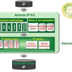
Manually validating the correctness of all but the smallest FSM is complex. Atrenta has developed an extension to its SpyGlass product family to address these FSM design and verification issues. SpyGlass Advanced Lint automatically recognizes FSMs, reports their metrics and checks for deadlock and unreachable states.

For more information read the white paper on Techniques for FSM Design and Verification.


A Brief History of Tensilica

A Brief History of Tensilica
by Daniel Nenni on 09-08-2012 at 7:00 pm

In the late 1990s, a change was going on in chip design. Companies had moved to system-on-chip design, which incorporated a general-purpose control processor plus blocks of logic (often called RTL) to do the hard tasks that the general-purpose processor couldn’t handle.

These blocks of logic were becoming a huge problem because of two major reasons:

[LIST=1]

  • They took a long time to design and even longer to verify that they worked properly. If they didn’t, the chip would have to be re-designed at huge expense.
  • They were inherently fixed-function blocks and couldn’t be programmed as standards or functions changed. When something changed, they had to be redesigned – another lengthy, costly process. And equipment already out in the field would be totally out of date.

    Chris Rowen, Tensilica’s founder, lived this challenge. As one of the founding employees of MIPS, he understood the challenges of designing a one-size-fits-all 32-bit RISC processor. He worked with MIPS’ customers, and understood their challenges designing hardware off-load logic blocks to do the work the processors couldn’t handle. And, as Sr. VP of the Design Re-use Business Unit at Synopsys, he understood the IP licensing business and the types of IP available to customers.

    Nothing like what Tensilica was inventing was available before. A couple of companies had experimented with opening their 32-bit RISC processor architecture to designers, but the designers had to figure out how to modify the processor themselves and then verify that the changes they made were correct. Then they had to modify all of the software tools to take advantage of the changes they had made in the processor. Only heavily trained processor designers and really good software teams could tackle this task.

    If a lot of these blocks of logic were going to be processor based for programmability, the entire way of designing these blocks and processors was going to have to change.

    So Tensilica started to develop an automated process for the development of new processor cores optimized to the intended application so they could take the place of these logic blocks. Tensilica started with a new, efficient 32-bit processor architecture as a base for all of their products, and then developed tools that would let companies optimize this architecture for their own needs.

    Tensilica has invested heavily in this fundamental technology, which also automates the creation of matching software tools that comprehend all customizations made to the processor cores. They guarantee that each core is automatically verified, cutting months off the verification cycle. They’ve been able to take the time to design a new processor core or block or logic down from 18-24 months to as little as a few hours. (To be honest, most of Tensilica’s customers take a few months just to take advantage of all of the optimizations possible – but it still significantly cut the design time and, more importantly, the verification time.)

    By customizing the processor, designers get a unique, one-of-a-kind core, complete with matching tool chain. So when they use it in a product, it can’t be easily copied. This is not a jelly bean processor core – it is part of a company’s intellectual property.

    Processors generated with Tensilica’s technology are used in everything from multi-million dollar central office routers to the latest smartphones. Tensilica’s processors are used for control, digital signal processing (DSP) and dataplane processing – anywhere lots of data needs to be processed quickly and efficiently.

    Tensilica has become the recognized leader in customizable dataplane processors. Dataplane Processor Units (DPUs) consist of performance intensive DSP (audio, video, imaging, and baseband signal processing) and embedded RISC processing functions (security, networking, and deeply embedded control). The automated design tools behind all of Tensilica’s application specific processor cores enable rapid customization to meet specific data plane performance targets.

    Huge companies have invested in Tensilica’s technology. Some of these companies even invested in Tensilica. Others have signed multi-million dollar contracts for Tensilica technology. Tensilica’s DSPs and processors power top tier semiconductor companies, innovative start-ups, and system OEMs for high-volume products including mobile phones, consumer electronics devices (including portable media players, digital TV, and broadband set top boxes), computers, and storage, networking and communications equipment.

    Take a look at the customer profiles page on the new Tensilica website. Almost 200 licensees with more than 2 billion cores shipped? The question is: when will Tensilica IPO? The answer will come next year I’m thinking.


  • Intel’s Haswell and the Tablet PC Dilemma

    Intel’s Haswell and the Tablet PC Dilemma
    by Ed McKernan on 09-07-2012 at 12:26 pm

    Paul Otellini’s greatest fear in his chase to have Intel win the Smartphone and Tablet space is that he opens the door to significant ASP declines in his current PC business. This is the Innovator’s Dilemma writ large. In 2011, Intel’s PC business (excluding servers) was $36B at an average ASP of $100. Within that model is an Ultra Low Voltage (ULV) product line that powers the Apple MAC Air and upcoming ultrabooks that sell for over $200. For 15 years, Intel placed a significant premium on low power because they yielded from the top speed bins and they were for a time, quite frankly, a nuisance. With the Ultrabook push, Intel was looking forward to being able to increase ASPs because they would garner more of the graphics content and not have AMD around as competition. However, Apple’s success with the iPAD using a $25 part at less than half of Ivy Bridge’s performance and running on older process technologies is upsetting Intel’s model. What comes next?
    Continue reading “Intel’s Haswell and the Tablet PC Dilemma”


    A brief history of Interface IP, the 4th version of IPNEST Survey

    A brief history of Interface IP, the 4th version of IPNEST Survey
    by Eric Esteve on 09-07-2012 at 5:17 am

    The industry is moving extremely fast to change the “old” way to interconnect devices using parallel bus, to the most efficient approach based on High Speed Serial Interconnect (HSSI) protocols. The use of HSSI has become the preferred solution compared with the use of parallel busses for new products developed across various segments. These new Interface functions are differentiated from the parallel bus based Interface like PCI by the use of High Speed Serial I/O, based on a multi-gigabit per second SerDes, this analog part interacting with the external world – the PHY. Another strong differentiation is the specification of packet based protocols, coming from the Networking world (think about ATM or Ethernet), requiring using a complex digital function, the Controller. PHY and Controller can be designed in-house, but both being at the leading edge of their respective technologies – Analog and Mixed-Signal (AMS) or Digital – the move to external sourcing of IP functions is becoming the trend.

    The list of the Interfaces technologies we will review is becoming longer almost every year: USB, PCI Express, HDMI, SATA, MIPI, DisplayPort, Serial RapidIO, Infiniband, Ethernet and DDRn. In fact, Infiniband and DDRn do not exactly fit with the definition given above, as the data are still sent in a parallel way, and the clock as a specific signal. But, the race for higher data bandwidth has pushed DDR4 bandwidth specification up to 2,133 Gb/s, which lead in practice to use a specific hard wired I/O (PHY) and require to use a controller, like for the other serial interfaces.

    IPNEST has proposed the first version of the “Interface IP Survey” back in 2009, as this specific IP market was already weighting $230 million in 2008, and was expected to grow with 10%+ CAGR for the next 5 to 7 years. The Interface IP was, and still is, a promising market (large size and still growing), attracting many new comers and generating good business for established companies like Synopsys, Denali (now Cadence) as well as for smaller companies like Virage Logic (now Synopsys), ChipIdea (now Synopsys), Arasan or PLDA, to name a few. The success of the survey came last year, with the 3[SUP]rd[/SUP] version, which has been sold to major IP vendors, but also to the smaller vendors, to ASIC Design Services companies and also to Silicon foundries, as well as to IDM and Fabless companies.

    What type of information could be found in the survey, and in the latest version, the 4[SUP]th[/SUP], issued these days? In fact, IPNEST is not only providing the market share information, protocol by protocol and year by year for 2006 to 2011 (when relevant), but do a real research work, in order to answer many other questions, which are the questions you try to answer when you are Marketing Manager for an IP vendor (I was in charge of this job for IP vendors), or when you are in charge of the Business development for an ASIC (Design Service or Foundry) company (that I did for TI and Atmel a while ago), or when you need to take the make-or-buy decision when managing a project for an IDM or fabless chip maker – and if the decision is finally to buy, who should I buy and at what price? The type of answers IPNEST customers find in the “Interface IP Survey” are:

    • 2012-2016 Forecast, by protocol, for USB, PCIe, SATA, HDMI, DDRn, MIPI, Ethernet, DisplayPort, based on a bottom-up approach, by design start by application
    • License price by type for the Controller (Host or Device, dual Mode)
    • License price by technology node for the PHY
    • License price evolution: technology node shift for the PHY, Controller pricing by protocol generation
    • By protocol, competitive analysis of the various IP vendors: when you buy an expensive and complex IP, the price is important, but other issues count as well, like

      • Will the IP vendor stay in the market, keep developing the new protocol generations?
      • Is the PHY IP vendor linked to one ASIC technology provider only or does he support various foundries?
      • Is one IP vendor “ultra-dominant” in this segment, so the success chance is weak, if I plan to enter this protocol market?

    These are precise questions that you need to answer before developing an IP, or buying it to integrate it in your latest IC, in both cases you’re most important challenge, whether you are IP vendor or chip maker. But the survey also address questions, for which a binary answer does not necessarily exist, but which gives you the guidance’s you need to select a protocol, and keep sure your roadmap will align with the market trends, and your customer needs. For example, if you develop for the storage market, you will not ignore SSD technology. But, when deciding to support SSD, will you interface it with SATA, SATA Express, NVM Express or homemade Nand Flash controller? Or, if you develop a portable electronic device for Consumer electronic market, should you jump start integrating MIPI technology now? For many of these questions, we propose answers, based on a 30 years industry experience, acquired in the field… That’s why also we have built for each survey a 5 years forecast, based on a bottom-up approach, that we propose with a good level of confidence to our customers, even if we know that any economic recession could heavily modify it.

    You probably better know why IPNEST is the leader on the IP dedicated surveys, enjoying this long customer list:

    For those who want to know more, you can read the height pages Introduction, extracted from the 4[SUP]th[/SUP] version of the “Interface IP Survey”, issue in August 2012, and proposed to Semiwiki readers very soon here.

    Eric Esteve from IPNEST –

    Table of Content for “Interface IP Survey 2006-2011 – Forecast 2012-2016” available here


    Have You Ever Heard of the Carrington Event? Will Your Chips Survive Another?

    Have You Ever Heard of the Carrington Event? Will Your Chips Survive Another?
    by Paul McLellan on 09-06-2012 at 9:07 pm

    In one of those odd coincidences, I was having dinner with a friend last week and somehow the Carrington Event came up. Then I read a a piece in EETimesabout whether electrical storms could cause problems in the near future. Even that piece didn’t mention the Carrington Event so I guess George Leopold, the author, hasn’t heard of it.

    It constantly surprises me that people in electronics have not heard of the Carrington Event, the solar storm of 1859. In fact my dinner companion (also in EDA) was surprised that I’d heard of it. But it is a “be afraid, be very afraid” type of event that electronics reliability engineers should all know about as a worst case they need to be immune to.

    Solar flares go in an 11-year cycle, aka the sunspot cycle. The peak of the current cycle is 2013 or 2014. This cycle is unusual for its low number of sunspots and there are predictions that we could be in for an extended period of low activity like the Maunder minimum from 1645-1715 (the little ice age when the Thames froze every winter) or the Dalton minimum from 1790-1830 (where the world was also a couple of degrees colder than normal). Global warming may be just what we need, it is cooling that causes famines.

    But for electronics, the important thing is the effect of coronal mass ejection which seems to cause solar flares (although the connection isn’t completely understood). Obviously the most vulnerable objects are satellites since they lack protection from the earth’s magnetic field. There was actually a major event in March but the earth was not aligned at a vulnerable angle and so nothing much happened and the satellites seemed to survive OK.

    But let’s go back to the Carrington Event. It took place from August 28th to September 2nd 1857. It was in the middle of a below average solar cycle (like the current one). There were numerous solar flares. One on September 1st, instead of taking the usual 4 days to reach earth, got here in just 17 hours, since a previous one had cleared out all the plasma solar wind.

    On September 1st-2nd the largest solar geomagnetic storm ever recorded occurred. We didn’t have electronics in that era to be affected but we did have telegraph by then. They failed all over Europe and North America, in many cases shocking the operators. There was so much power that some telegraph systems continued to function even after they had been turned off.

    Aurora Borealis (Northern Lights) was visible as far south as the Caribbean. It was so bright in places that people thought dawn had occurred and got up to go to work. Apparently it was bright enough to read a newspaper.

    Of course telegraph systems stretch for hundreds or thousands of miles so have lots of wire to intercept the fields. But the voltages involved seemed to be huge. It doesn’t seem that different from the magnetic pulse of a nuclear bomb. And these days, our power grids are huge, and connected to everything except our portable devices.

    Imagine the chaos if the power grid shuts down, if datacenters go down, if chips in every car’s engine-control-unit fries or and all our cell-phones stop working. And even if your cell-phone survives and there is no power, you don’t have that long before its battery is out. It makes you realize just how dependent we are on electronics continuing to work.

    In 1859 telegraph systems were down for a couple of days and people got to watch some interesting stuff in the sky. But from a NASA event last year in Washington looking at what would happen if another Carrington Event occured:In 2011 the situation would be more serious. An avalanche of blackouts carried across continents by long-distance power lines could last for weeks to months as engineers struggle to repair damaged transformers. Planes and ships couldn’t trust GPS units for navigation. Banking and financial networks might go offline, disrupting commerce in a way unique to the Information Age. According to a 2008 report from the National Academy of Sciences, a century-class solar storm could have the economic impact of 20 hurricane Katrinas.

    Actually, to me, it sounds a lot worse than that. More like Katrina hitting everywhere, not just New Orleans. That’s a lot more than 20. To see how bad a smaller event can be:In March of 1989, a severe solar storm induced powerful electric currents in grid wiring that fried a main power transformer in the HydroQuebec system, causing a cascading grid failure that knocked out power to 6 million customers for nine hours while also damaging similar transformers in New Jersey and the United Kingdom.

    Wikipedia on the Carrington Event is here. The discussion at NASA here.


    Built to last: LTSI, Yocto, and embedded Linux

    Built to last: LTSI, Yocto, and embedded Linux
    by Don Dingee on 09-06-2012 at 8:30 pm

    The open source types say it all the time: open is better when it comes to operating systems. If you’re building something like a server or a phone, with either a flexible configuration or a limited lifetime, an open source operating system like Linux can put a project way ahead.

    Linux has always started with a kernel distribution, with a set of features ported to a processor. Drivers for common functions, like disk storage, Ethernet, USB, and OpenGL graphics were abstracted enough so they either dropped in or were easily ported. Support for new peripheral devices usually emerged from the community very quickly. Developers grew to love Linux because it gave them, instead of vendors, control.

    Freedom comes with a price, however. In the embedded world, where change can be costly and support can be the never-ending story over years and even decades, deploying Linux has not been so easy. Mind you, it sounds easy, until one thing becomes obvious: Linux has been anything but stable when viewed over a period of years. Constant innovation from the community means the source tree is a moving target, often changing hourly. What was built yesterday may not be reproducible today, much less a year from now.

    The first attempts at developing embedded Linux involved “freezing” distributions, which produced a stable point configuration. A given kernel release with support for given peripherals could be integrated, built and tested, and put into change control and released. In moderation this worked well, but after about 100 active products showed up in a lab with 100 different frozen build configurations, the scale of juggling became problematic. Without the advantage of being able to retire obsolete configurations, Linux started becoming less attractive for longer lifecycles, and embedded developers were forced to step back and look harder.

    In what the folks at The Linux Foundation have termed “the unholy union of innovation and stability”, best brains are trying to bring two efforts – defining what to build and how to build it – to bear to help Linux be a better choice for embedded developers.

    LTSI, the Long Term Support Initiative, is backed by many of the companies we discuss regularly here, including Intel, Mentor Graphics, NVIDIA, Qualcomm, and Samsung. LTSI seeks to create a stable tree appropriate for consumer devices living 2 to 3 years, and yet pick up important new innovations in a road-mapped effort. The goal is to “reduce the number of private [Linux] trees current in use in the CE industry, and encourage more collaboration and sharing of development resources.”

    The Yocto Project focuses on tools, templates, and methods to build a Linux tree into an embedded distribution. This doesn’t sound like a breakthrough until one considers that almost all embedded development on Linux has been roll-your-own, and as soon as a development team deviates and does something project specific to meet their needs, they lose the benefits of openness because they can’t pull from the community without a big retrace of their steps. The Yocto Project recently announced a compliance program, with Mentor Graphics among the first companies to comply, and Huawei, Intel, Texas Instruments and others participating and moving toward compliance. Yocto has also announced a joint roadmap with LTSI.

    With software becoming a larger and larger part of projects – some say 70% and growing – and open source here to stay, these initiatives seek to help Linux be built to last.


    The GLOBALFOUNDRIES Files

    The GLOBALFOUNDRIES Files
    by Daniel Nenni on 09-06-2012 at 9:58 am

    There’s a new blogger in town, Kelvin Low from GLOBALFOUNDRIES. Kelvin was a process engineer for Chartered Semiconductor before moving on to product marketing for GF. His latest post talks about the GF 28nm SLP which is worth a read. There was quite the controversy over this Gate-First HKMG implementation of 28nm that IBM/GF/Samsung uses versus the Intel and TSMC Gate-Last implementation. One of the benefits of the GF version being very low power:

    SLP targets low-power applications including cellular base band, application processors, portable consumer and wireless connectivity devices. SLP utilizes HKMG and presents a 2x gate density benefit, but is a lower cost technology in terms of the performance elements utilized to boost carrier mobilities.

    Anyway, Kelvin is a great addition to GF’s Mojy Chian and Michael Noonan. I look forward to reading more about customer applications at 28nm and beyond.

    28nm-SLP technology – The Superior Low Power, GHz Class Mobile Solution
    Posted on September 4, 2012
    By Kelvin Low
    In my previous blog post, I highlighted our collaborative engagement with Adapteva as a key factor in helping them deliver their new 64-core Epiphany-4 microprocessor chip. Today I want to talk about the second key ingredient in enabling their success: the unique features of our

    28nm-SLP technology: Enabling Innovation on Leading Edge Technology
    Posted on August 30, 2012
    By Kelvin Low
    It’s always great to see a customer celebrate their product success, especially when it’s developed based on a GLOBALFOUNDRIES technology. Recently, one of our early lead partners, Adapteva, announced sampling of their 28nm 64-core Epiphany-4 microprocessor chip. This chip is designed on our 28nm-SLP technology which offers the ideal balance of low power, GHz class performance and optimum cost point. I will not detail the technical results of the chip but will share a quote by Andreas Olofsson, CEO of Adapteva, in the recent company’s press release…

    Innovation in Design Rules Verification Keeps Scaling on Track
    Posted on August 28, 2012
    By Mojy Chian
    There is an interesting dynamic that occurs in the semiconductor industry when we talk about process evolution, roadmaps and generally attempt to peer into the future. First, we routinely scare ourselves by declaring that scaling can’t continue and that Moore’s Law is dead (a declaration that has happened more often than the famously exaggerated rumors of Mark Twain’s death). Then, we unfailingly impress ourselves by coming up with solutions and workarounds to the show-stopping challenge of the day. Indeed, there has been a remarkable and consistent track record of innovation to keep things on track, even when it appears the end is surely upon us…

    Breathing New Life into the Foundry-Fabless Business Model
    Posted on August 21, 2012
    By Mike Noonen
    Early last week, GLOBALFOUNDRIES jointly announced with ARM another important milestone in our longstanding collaboration to deliver optimized SoC solutions for ARM® processor designs on GLOBALFOUNDRIES’ leading-edge process technology. We’re extending the agreement to include our 20nm planar offering, next-generation 3D FinFET transistor technology, and ARM’s Mali™ GPUs…

    Re-defining Collaboration
    Posted on July 18, 2012
    By Mojy Chian
    The high technology industry is well known for its use – and over-use – of buzzwords and jargon that can easily be rendered meaningless as they get saturated in the marketplace. One could argue ‘collaboration’ is such an example. While the word itself may seem cliché, the reality is that what it stands for has never meant more…


    Wireless Application: DSP IP core is dominant

    Wireless Application: DSP IP core is dominant
    by Eric Esteve on 09-06-2012 at 5:32 am

    If we look back in the early 90’s, when the Global System for Mobile Communication (GSM) standard was just an emerging technology, the main innovation was the move from Analog to the Digital Processing of the Signal (DSP), allowing to make unlimited manipulation to an Analog signal, once digitized by the means of a converter (ADC). To run the Digital baseband Processing (see picture), the system designer had to implement the Vocoder, Channel codec, Interleaving, Ciphering, Burst formatting, Demodulator and (Viterbi) Equalizer. Digital Signal Processing science was already heavily used for military application like Radar, but was emerging in telecommunication. The very first GSM mobile handset built based on standard part (ASSP) were using no less than three TI 320C25 DSP, each of them costing several dozen of dollar!

    Very quickly, it appears that the chip makers developing IC for mobile handset baseband processing should rely on ASIC technology rather than using ASSP, for two major reasons: cost and power consumption. As one company was dominating the DSP market, Texas Instruments, the mobile handset manufacturers, Ericsson, Nokia and Alcatel had to push TI to propose a DSP core, which could be integrated into an ASIC, developed by the above mentioned OEM. During the years 1995 to early 2000’s, thanks to their dominant position in DSP market, TI was the undisputed leader in manufacturing the baseband processor, through ASIC technology, for the GSM handset OEM, who also developed the IC, at that time.

    But a small company named DSP Group, had appeared in the late 90’s, proposing a DSP IP core, not linked to any existing DSP vendor (TI, Motorola or Analog Devices), and even more important, to any ASIC technology vendor. The merge of the IP licensing division of DSP Group and Parthus has been named CEVA and CEVA’ DSP was specially tailored for the wireless handset application. TI competition (VSLI Technology, STMicroelectronics and more) was certainly happy as they could propose an alternative solution to the Nokia et al., but it took some time before these OEM decide to move the S/W installed base from TI DSP to CEVA DSP IP core, that they had to do if they decide to move from TI to another supplier. It was a long route, but CEVA is enjoying today most of the Application Processors chip maker leaders in their customer list, namely:

    This help to understand why CEVA has enjoyed 70% market share for DSP IP products in 2011, according with the Linley Group. A 70% market share simply means that CEVA’ DSP IP have been integrated into 1 billion IC shipped in production in 2011! If the Teak DSP IP core was the company flagship in early 2000, the ever increasing need for digital signal processing power associated with 3G and Long Term Evolution (LTE or 4G) has led to propose various new products, the latest being CEVA XC4000 DSP IP core:

    And, by the way, the XC4000 target various applications, on top of the wireless handset:

    • Wireless Infrastructure

    A scalable solution for Femtocells up to Macrocells

    • Wireless connectivity

    A single platform for: Wi-Fi 802.11a/b/g/n/ac, GNSS, Bluetooth and more

    • Universal DTV Demodulator

    A programmable solution targeting digital TV demodulation in software
    Target standards: DVB-T, DVB-T2, ISDB-T, ATSC, DTMB, etc.

    • SmartGrid

    A single platform for: wireless PAN (802.11, 802.15.4, etc.), PLC (Power Line Communication), and Cellular communication (LTE, WCMDA, etc.)

    • Wireless Terminals

    Handsets, Smartphones, Tablets, data cards, etc.
    Addressing: LTE, LTE-A, WiMAX, HSPA/+, and legacy 2G/3G standards

    If we look at the Wireless handset market, it appears that Smartphone and Media tablet, both being based on the same SoC, the Application Processor, will represent the natural evolution, and the analysts forecast the shipment of one billion Smartphone and 200 million Media tablets in 2015. If you look more carefully, you will discover that at least 50%, if not the majority of these devices will be shipped in ASIA, and to be more specific, in China for most of these. An IP vendor neglecting China today would certainly decline in a few years. Looking again at CEVA’s customer list, we can see that many of the Application Processor chip makers selling in these new “Eldorado” markets have selected CEVA. This is a good sign that CEVA will maintain their 70% market share of the DSP IP market in the future!

    Like ARM IP core is coming in mind immediately when you consider a CPU core for Application Processor wireless handset phone or smartphone, CEVA DSP IP is the dominant solution for the same. Just a final remark: CEVA is claiming to have design-in their DSP IP in the Chinese version of the Samsung Galaxy S3, which will probably be the most selling smartphone on a world-wide basis…

    Eric Esteve from IPNEST