Synopsys IP Designs Edge AI 800x100

Designing with FinFETs

Designing with FinFETs
by Daniel Payne on 10-08-2012 at 6:13 pm

Intel is the number one semiconductor company in the world and has taken the lead in bringing FinFET (aka Tri-Gate) silicon to market at the 22nm node starting in May 2011, so now we see the pure play foundries playing catch-up and start talking about their own FinFET roadmaps. IC designers and layout engineers want to know how their design methodology will change as they consider using a FinFET process compared to a planar process.

Jamil Kawa
at Synopsys has just written a new White Paper, Designing with FinFETs: The Opportunities and the Challenges. This blog summarizes the major points of the White Paper on FinFETs and how it effects the IC design process.


Source: Intel

There’s a bit of marketing hype in the Intel statement of transistors now entering the third dimension because all planar transistors have three dimensions, it’s just that the FinFET is notably taller than planar CMOS transistors.


Simplified transistor comparison not drawn to scale, Planar vs FinFET

Attractive features of the FinFET transistors include:

  • Lower leakage currents caused by a fully depleted channel region
  • Reduced short-channel effects
  • More transistors/unit area due to 3D layout
  • Less variation effects from dopant fluctuation
  • Lower Line Edge Roughness (LER) variation
  • Improved performance margins
  • Lower retention voltage in SRAMs


Intel’s 22nm Tri-Gate technology showing a wider performance advantage at lower VDD
Source: Mark Bohr, Intel. May 2011.

Negative consequences of using FinFET devices are:

  • Quantized channel widths, fewer choices compared to planar CMOS
  • More complex SPICE models, longer simulation run times
  • More complex extraction rules and longer extraction run times
  • Body-biasing techniques lose their effectiveness
  • Additional Restricted Design Rules (RDR)
  • New Layout Proximity Effects (LPE)
  • Reliability concerns, Negative-Bias Temperature Instability (NBTI) and Positive-Bias Temperature Instability (PBTI)


Stress simulation of FinFETs


Parasitics model of the FinFET

With the increased number of layout rules for FinFET devices you want to use a rule-driven layout flow, instead of the old sequential flow of: Schematic design, Layout design, batch rule check, iterate until correct.

EDA Tool Flow
Synopsys has seven EDA tools used to implement FinFET-based IC designs:

[TABLE] style=”width: 500px”
|-
| EDA Category
| EDA Tool
|-
| TCAD modeling
| Sentaurus
|-
| Parasitic extraction
| StarRC
|-
| SPICE circuit simulation
| HSPICE, CustomSim
|-
| IC schematic and layout editing
| Custom Designer
|-
| DRC and LVS checking
| IC Validator
|-
| Implementation (Logic Synthesis, P&R)
| Galaxy
|-
| Mask synthesis
| Proteus
|-

Summary
Intel started using FinFET devices at the 22nm node in 2011 while other foundries have announcements for FinFETs at 14nm nodes coming up in 2013 and later. EDA tool flows have been updated to account for the new FinFET issues, so the big question that remains is silicon pricing and yield compared to planar technology.

Read the complete White Paper here after a brief registration process.

Related Reading


ReRAM Cell Switching and Trends

ReRAM Cell Switching and Trends
by Ed McKernan on 10-08-2012 at 11:41 am


Confused by the way a ReRAM cell behaves? Looking for a clear definition of the various terms used? Then check out Blogs at ReRAM-Forum.com. on recent publications appearing in the IEEE journals. The latest Blog discusses a paper published by Professor Daniele Ielmini of the Politecnico di Milano in Italy on the Resistive Switching by Voltage-Driven Ion Migration in Bipolar RRAM. The paper repays a careful read and the Blog captures some of the highlights particularly with respect to the way that ReRAM cell set and reset processes interact. For more information, head over to www.ReRAM-Forum.com


SOI need a large IP Ecosystem, 100% Reliable Novocell NVM IP is now part of IBM SOI 32nm ecosystem

SOI need a large IP Ecosystem, 100% Reliable Novocell NVM IP is now part of IBM SOI 32nm ecosystem
by Eric Esteve on 10-08-2012 at 9:16 am

When a company develops chip for the military industry, I would prefer these chips to be using a 100% reliable technology. I am sure that you too! For certain application, 99%, or even 99.99% rate of confidence is not enough. Would you accept to fly in an airplane if you still have 1 out of 10,000 chances to crash? Would you accept living in an area which could be destroyed by one of this very “efficient” atomic bomb, even knowing at 99.99% that it shouldn’t happen?

That’s why it’s good to hear that a “United States military contractor has decided to adopt the 100% reliable Smartbit™-based non-volatile memory (NVM), a one-time programmable (OTP) antifuse product from Novocell, taped out in a 32nm SOI process at IBM’s foundry”. All Novocell Smartbit-based NVM IPproducts avoid the limitations of traditional embedded NVM technology by utilizing the patented design and dynamic programming and monitoring process of the Novocell Smartbit bit cell, ensuring that 100% of customers’ embedded bit cells are fully programmed. The result is Novocell’s unmatched 100% yield and unparalleled reliability, guaranteeing customers that their data is fully programmed initially, and will remain so for an industry-leading 30 years or more. We have explained in Semiwiki the mechanisms allowing Novocell to claim this 100% reliability: “breakdown detector” circuitry, checking that hard breakdown as effectively occurred.

The point to be highlighted is that Smartbit technology has been ported on chips based on IBM’s 32nm, Silicon-on-Insulator (SOI) technology, which was jointly developed with GLOBALFOUNDRIES and other members of IBM’s Process Development Alliance, with early research at the University at Albany’s College of Nanoscale Science and Engineering. The technology vastly improves microprocessor performance in multi-core designs and speeds the movement of graphics in gaming, networking, and other image intensive, multi-media applications. The SOI process was used to build the microprocessor that powered IBM Watson, the question-answering computer that won the Jeopardy! quiz show in early 2011.

When I look back at my very first job in SC industry, it was with Philips Research Lab (LEP), trying to identify and characterize EL2 traps in GaAs substrate by measuring current flow within a handmade diode (I remember I had to hard wire the diode using a golden wire soldered under a microscope!…FYI, the picture is of the very first integrated circuit handmade by Jack Kilby).

When I asked my manager why Philips was spending so much money on GaAs although Silicon was much easier to process, the answer was: because the electron mobility was higher by a factor of five (I already knew it from University), allowing running the devices at higher frequency, AND because GaAs substrate is nonconductor, or, if you prefer insolent. What are the benefits? At first, no leakage current in the substrate, this part of the power consumption which tend to be higher when the technology node decrease. We can see today with the latest technologies (28 or 20 nm) that the power dissipation tends to stay flat instead of decreasing, due to this effect.

The second benefit, I could really appreciate it when doing my PhD later on, studying the parasitic resistor and capacitor on CMOS (Silicon) technology: the delay in any interconnects wire can be simply modeled as an RC delay. To change the resistivity value (the R) you can change the wire material, but the capacitor value is directly linked with the substrate conductivity: it will be much lower if the substrate is insolent. At the time I was measuring and modeling this effect, the delay lost in interconnects was about a few % of the gate delay. The impact of the delay spent in interconnects has dramatically increased in proportion: the technology feature size has decreased by a factor of 100 (2um to 20nm), so approximately the gate delay, when the interconnect delay tend to stay flat. Thus, the proportion has passed from a few % to a few times! If you could suppressed or strongly decrease the capacitance (the “C” in the RC), you could better benefit from the technology downscaling (Moore’ law).

As a matter of fact, Philips Research Lab could never successfully create a GaAs oxide (like SiO2, easy to create for the Silicon), thus the GaAs usage to build Large Scale of Integration (LSI) device was not practically possible, and the technology has only been used to process discrete devices, but unfortunately not to process SoC. If you want to build a SoC and benefit from an insolent substrate, the Silicon On Insulator (SOI) technology is the only route today. But, if you want the technology to be successful, you need to benefit from an IP Ecosystem as large as possible, and Smartbit is one piece of this Ecosystem.

Eric Esteve from IPNEST –


Silicon Correlation, Not EDA Marketing Sparkles!

Silicon Correlation, Not EDA Marketing Sparkles!
by Daniel Nenni on 10-07-2012 at 9:00 pm

It’s all about the silicon. It’s all about silicon correlation. TSMC Open Integration Platform should be renamed TSMC Silicon Correlation Platform or TSMC SCP. One of the problems I have with EDA technical papers today is that they are not silicon based. Anybody can put up slides with marketing sparkles on them but if you want qualified people to attend your presentation SHOW US THE SILICON CORRELATION!

Looking at the TSMC OIP papers this year you will see a trend of silicon correlation. TheBDA paper with Analog Bits for example. No marketing sparkles here, this one is on production high speed 28nm silicon:

Design Methodology for SiliconAccurate Jitter Analysis
for 28nm Interface IP for 100GB Applications

The successful design of a SerDes for 100GB Ethernet applications requires providing accurate quadrature outputs from a highperformance PLL at very low dissipated power levels. This paper describes the design and verification methodology of a 14GHz SerDes PLL for 100GB applications fabricated in TSMC 28nm technology which produces quadrature outputs and a measured output clock jitter < 0.3ps rms in under 12mW of power. The circuit verification methodology used to complete the jitter analysis relies on Berkeley Design Automation Analog FastSPICE (AFS) Platform and includes analysis of all device noise contributions, sensitivity analysis, RC parasitics, PVT and mismatch variations. The AFS Platform is certified in TSMC SPICEQualification Program, and AFS device noise subflow validated in TSMC AMS Reference Flow 2.0.

In this paper, we first review the design requirements for a SerDes IP macro for 100GB Ethernet applications, the OIFCEI28G*specifications, and the corresponding requirements on the highperformance PLL to meet the stringent jitter specifications. We describe the key effects that must be captured in any analysis to provide an estimate of the phase noise and jitter expected in TSMC 28nm technology. These include the impact of device noise, the identification of the top noise contributors, the capture of all postlayout effects, comprehensive PVT, and mismatch analysis using the AFS Platform.

We compare the alternate methods available to analyze phase noise and jitter (both random and deterministic) and summarize the advantages and disadvantages of each method. We first begin by looking at a traditional blocklevel analysis approach, using postlayout analysis results for each of the key components and using a linear transfer function model to complete the analysis. We then look at a new fullloop simulation approach using transient noise analysis. By using a systematic approach using new characterization techniques availble in the AFS Platform, we are able to achieve a fast turnaroundtime to complete a comprehensive analysis.

We then present the results for phase noise and jitter analysis and illustrate the excellent results obtained via the new fullloop simulation approach using AFS Transient Noise analysis. We demonstrate phase noise results with excellent correlation to silicon measurements to within 3 dB in the frequency ranges of interest. The resulting methodology extending simulationtosilicon correlation is now a standard practice for the development of our 28nm and 20nm interface IPs.


The TSMC Open Innovation Platform® (OIP) Ecosystem Forum brings TSMC’s design ecosystem member companies together to share with our customers real-case solutions for customers’ design challenges and success stories of best practice in TSMC’s design ecosystem.

More than 90% of the attendees last year said “this forum helped them better understand the components of TSMC’s Open Innovation Platform” and “they found it effective to hear directly from TSMC OIP member companies.”

This year, the forum will feature a day-long conference starting with executive keynotes from TSMC and ARMin the morning plenary session to outline future design challenges and roadmaps, as well as discuss a recent collaboration announcement, 30 selected technical papers from TSMC’s EDA, IP, Design Center Alliance and Value Chain Aggregator member companies, and an Ecosystem Pavilion featuring up to 80 member companies showcasing their products and services.


TSMC OIP Ecosystem Forum 2012

TSMC OIP Ecosystem Forum 2012
by Daniel Nenni on 10-07-2012 at 7:11 pm

The TSMC Open Innovation Platform® (OIP) Ecosystem Forum brings TSMC’s design ecosystem member companies together to share with our customers real-case solutions for customers’ design challenges and success stories of best practice in TSMC’s design ecosystem.


More than 90% of the attendees last year said “this forum helped them better understand the components of TSMC’s Open Innovation Platform” and “they found it effective to hear directly from TSMC OIP member companies.”

Please introduce yourself if you see me. It would be a pleasure to meet you!

REGISTRATION

This year, the forum will feature a day-long conference starting with executive keynotes from TSMC and ARMin the morning plenary session to outline future design challenges and roadmaps, as well as discuss a recent collaboration announcement, 30 selected technical papersfrom TSMC’s EDA, IP, Design Center Alliance and Value Chain Aggregator member companies, and an Ecosystem Pavilion featuring up to 80 member companies showcasing their products and services.

Agenda

San Jose Convention Center,
Tuesday , October 16th, 2012

[TABLE] cellpadding=”4″ style=”width: 97%”
|-
| colspan=”4″ align=”center” | Plenary Session
|-
| style=”width: 15%” | 08:00
| colspan=”3″ | Registration Opens
|-
| 09:00 – 09:10
| colspan=”2″ | Welcome Remarks
| style=”width: 29%” | TSMC NA Executive
|-
| 09:10 – 09:40
| colspan=”2″ | An Ecosystem for Innovation
| TSMC Executive
|-
| 09:40 – 10:10
| colspan=”2″ | TSMC Design Technology Update
| TSMC Executive
|-
| 10:10 – 10:40
| colspan=”2″ | ARM Feature Talk
| Inviting Executive Level Speaker
|-
| 10:40 – 11:00
| colspan=”3″ align=”center” | Coffee Break
|-

[TABLE] cellpadding=”4″ style=”width: 97%”
|-
| align=”center” style=”width: 15%” | [TABLE] cellpadding=”10″ style=”width: 100%”
|-
| align=”center” |
|-

| align=”center” width=”27%” | EDA Track
| align=”center” width=”29%” | IP Track
| align=”center” width=”29%” | EDA/IP/Services Track
|-
| 11:00 – 11:30
| align=”center” valign=”top” | [TABLE] cellspacing=”3″ style=”width: 100%”
|-
| align=”center” valign=”top” | A Platform for the CoWoS Reference Flow
|-
| align=”center” valign=”top” | Mentor Graphics
|-

| align=”center” valign=”top” | [TABLE] cellspacing=”3″ style=”width: 100%”
|-
| align=”center” valign=”top” | TSMC IP Kit V2.0 – Enhancing Soft IP Quality Standards
|-
| align=”center” valign=”top” | Atrenta
|-

| align=”center” valign=”top” | [TABLE] cellspacing=”3″ style=”width: 100%”
|-
| align=”center” valign=”top” | SiP, 3D-IC & IPD Complement Flexible ASICs
|-
| align=”center” valign=”top” | GUC
|-

|-
| 11:30 – 12:00
| align=”center” valign=”top” | [TABLE] cellspacing=”3″ style=”width: 100%”
|-
| align=”center” valign=”top” | How to Manage Variability and Double
Patterning at 20nm
|-
| align=”center” valign=”top” | Cadence
|-

| align=”center” valign=”top” | [TABLE] cellspacing=”3″ style=”width: 100%”
|-
| align=”center” valign=”top” | 1T-OTP – Non-Volatile Memory for
Mobile and Other Low-Power Applications
|-
| align=”center” valign=”top” | Sidense
|-

| align=”center” valign=”top” | [TABLE] cellspacing=”3″ style=”width: 100%”
|-
| align=”center” valign=”top” | Timing Sign-off and Technology Migration Using Functionalized Timing Reports
|-
| align=”center” valign=”top” | IMEC
|-

|-
| 12:00 – 12:30
| align=”center” valign=”top” | [TABLE] cellspacing=”3″ style=”width: 100%”
|-
| align=”center” valign=”top” | Finding and Fixing Double Patterning Errors in 20nm Design
|-
| align=”center” valign=”top” | Mentor Graphics &
TSMC

|-

| align=”center” valign=”top” | [TABLE] cellspacing=”3″ style=”width: 100%”
|-
| align=”center” valign=”top” | Implementing and Optimising Graphics IP in SoCs
|-
| align=”center” valign=”top” | Imagination Technologies
|-

| align=”center” valign=”top” | [TABLE] cellspacing=”3″ style=”width: 100%”
|-
| align=”center” valign=”top” | Truly Differentiated Memory Subsystems on TSMC’s Advanced Technology Nodes
|-
| align=”center” valign=”top” | eSilicon
|-

|-
| 12:30 – 13:30
| colspan=”3″ align=”center” valign=”top” | Lunch
|-
| 13:30 – 14:00
| align=”center” valign=”top” | [TABLE] cellspacing=”3″ style=”width: 100%”
|-
| align=”center” valign=”top” | Enabling 20nm Custom Design in Laker
|-
| align=”center” valign=”top” | Springsoft
|-

| align=”center” valign=”top” | [TABLE] cellspacing=”3″ style=”width: 100%”
|-
| align=”center” valign=”top” | Advanced Silicon Design Methodology For Achieving 20nm Ready, Physical IP
|-
| align=”center” valign=”top” | Synopsys
|-

| align=”center” valign=”top” | [TABLE] cellspacing=”3″ style=”width: 100%”
|-
| align=”center” valign=”top” | Publishing Innovation through IP Targeting TSMC Technology
|-
| align=”center” valign=”top” | Design & Reuse
|-

|-
| 14:00 – 14:30
| align=”center” valign=”top” | [TABLE] cellspacing=”3″ style=”width: 100%”
|-
| align=”center” valign=”top” | 3D-IC Silicon Interposer IC Design Flow Using Cadence Encounter Digital Implementation (EDI) System
|-
| align=”center” valign=”top” | Cadence
|-

| align=”center” valign=”top” | [TABLE] cellspacing=”3″ style=”width: 100%”
|-
| align=”center” valign=”top” | Comprehensive Embedded NVM Solution in Trusted Technology and Capacity Platform
|-
| align=”center” valign=”top” | eMemory
|-

| align=”center” valign=”top” | [TABLE] cellspacing=”3″ style=”width: 100%”
|-
| align=”center” valign=”top” | TMI: A Unified Compact Model Development Platform for 28nm & Beyond
|-
| align=”center” valign=”top” | Synopsys &
TSMC

|-

|-
| 14:30 – 15:00
| align=”center” valign=”top” | [TABLE] cellspacing=”3″ style=”width: 100%”
|-
| align=”center” valign=”top” | Verification of Power, Signal, and Reliability Integrity for 3D-IC/Silicon Interposer Designs
|-
| align=”center” valign=”top” | ANSYS / Apache
|-

| align=”center” valign=”top” | [TABLE] cellspacing=”3″ style=”width: 100%”
|-
| align=”center” valign=”top” | Novel Low-Power Audio CODEC from 180nm to 28nm with Moore and More!
|-
| align=”center” valign=”top” | Dolphin Integration
|-

| align=”center” valign=”top” | [TABLE] cellspacing=”3″ style=”width: 100%”
|-
| align=”center” valign=”top” | Design Methodology for Silicon-Accurate Jitter Analysis for 28nm Interface IP for 100GB Applications
|-
| align=”center” valign=”top” | Berkeley Design Automation &
Analog Bits

|-

|-
| 15:00 – 15:30
| colspan=”3″ align=”center” | Coffee Break
|-
| 15:30 – 16:00
| align=”center” valign=”top” | [TABLE] cellspacing=”3″ style=”width: 100%”
|-
| align=”center” valign=”top” | TSMC Certification for Cadence 20nm RTL-to-GDSII Flow
|-
| align=”center” valign=”top” | Cadence
|-

| align=”center” valign=”top” | [TABLE] cellspacing=”3″ style=”width: 100%”
|-
| align=”center” valign=”top” | Solving ESD, EOS and Latch-Up Requirements
– For Analog Interfaces in Advanced CMOS
– For Automotive Applications in TSMC’s BCD Platforms
|-
| align=”center” valign=”top” | SOFICS
|-

| align=”center” valign=”top” | [TABLE] cellspacing=”3″ style=”width: 100%”
|-
| align=”center” valign=”top” | Comprehensive Simulation and Modeling Solutions for TSMC’s RF Platforms
|-
| align=”center” valign=”top” | Agilent / EEsof
|-

|-
| 16:00 – 16:30
| align=”center” valign=”top” | [TABLE] cellspacing=”3″ style=”width: 100%”
|-
| align=”center” valign=”top” | Double-Patterning Technology and Impact on 20nm Designs
|-
| align=”center” valign=”top” | Synopsys
|-

| align=”center” valign=”top” | [TABLE] cellspacing=”3″ style=”width: 100%”
|-
| align=”center” valign=”top” | Enabling Design with Advanced Node Design IP for TSMC
|-
| align=”center” valign=”top” | Cadence
|-

| align=”center” valign=”top” | [TABLE] cellspacing=”3″ style=”width: 100%”
|-
| align=”center” valign=”top” | Silicon-Accurate Mixed-Signal Fractional-N PLL IP Design
|-
| align=”center” valign=”top” | Berkeley Design Automation &
Silicon Creations

|-

|-
| 16:30 – 17:00
| align=”center” valign=”top” | [TABLE] cellspacing=”3″ style=”width: 100%”
|-
| align=”center” valign=”top” | Improved Design for Reliability Using Calibre PERC
|-
| align=”center” valign=”top” | Mentor Graphics
|-

| align=”center” valign=”top” | [TABLE] cellspacing=”3″ style=”width: 100%”
|-
| align=”center” valign=”top” | Kilopass Roadmap for Advanced TSMC Processes
|-
| align=”center” valign=”top” | Kilopass
|-

| align=”center” valign=”top” | [TABLE] cellspacing=”3″ style=”width: 100%”
|-
| align=”center” valign=”top” | Chip-Partitioning Trends in Systems Using Ultra Deep-Submicron SoCs
|-
| align=”center” valign=”top” | Cosmic Circuits
|-

|-
| 17:00 – 17:30
| align=”center” valign=”top” | [TABLE] cellspacing=”3″ style=”width: 100%”
|-
| align=”center” valign=”top” | Automated Approach for Waiving Physical Verification Errors at IP
|-
| align=”center” valign=”top” | Mentor Graphics &
LSI

|-

| align=”center” valign=”top” | [TABLE] cellspacing=”3″ style=”width: 100%”
|-
| align=”center” valign=”top” | Using Latest-Generation DDR4, LPDDR3 and
Wide-IO DRAM Devices with Chips in TSMC’s
Advanced 28nm and 20nm Processes
|-
| align=”center” valign=”top” | Cadence
|-

| align=”center” valign=”top” | [TABLE] cellspacing=”3″ style=”width: 100%”
|-
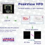
| align=”center” valign=”top” | CMOS Silicon Millimeterwave Design Closure on
Integrated Fullwave Electromagtic Simulation and
Extraction Platform with a Real Silicon Design Case
|-
| align=”center” valign=”top” | Lorentz &
Stanford University

|-

|-
| 17:30 – 18:00
| colspan=”3″ align=”center” | Networking and Reception
|-

Legal Notice:TSMC is not responsible for the content, accuracy, or reliability of any of the presentations at the TSMC Open Innovation Platform Ecosystem Forum. Furthermore, posting the presentation abstracts on TSMC’s corporate website does not constitute an endorsement of the content of those presentations by TSMC. Any liability arising from the contents of any of the presentations is the responsibility of the presenter itself, and not TSMC.


Apache Dimensions of Electronic Design Seminars

Apache Dimensions of Electronic Design Seminars
by Paul McLellan on 10-07-2012 at 1:17 pm

Coming up are ANSYS/Apache seminars on Dimensions of Electronic Design. Watch the video where Arvind Shanmugavel gives some details about why you should attend. Probably most readers are in Silicon Valley, and the seminar here is on 18th at the Hyatt (next to Santa Clara convention center).

The seminars are free to qualified attendees. However, seating is limited so you must sign up in advance. The registration page is here.

There are four seminars currently scheduled:

  • Thursday October 11th at Sheraton Framingham MA. Detailed agenda.
  • Thursday October 18th at Hyatt Regency Santa Clara CA. Detailed agenda.
  • Wednesday October 24th at Manhattan Beach Marriott CA. Detailed agenda.
  • Thursday November 1st at Hyatt Regency Austin TX. Detailed agenda.


Design Automation Conference 2013 Austin, Texas Call for Papers!

Design Automation Conference 2013 Austin, Texas Call for Papers!
by Daniel Nenni on 10-07-2012 at 9:00 am

DAC’s technical program offers the best-in-class solutions that promise to advance Electronic Design Automation (EDA) and Embedded Systems and Software (ESS). DAC 2013 is seeking submissions that deal with design technologies and algorithms, addressing all aspects of electronic design across several submission categories.

The Design Automation Conference (DAC) is recognized as the premier event for the design of electronic circuits and systems and for electronic design automation (EDA) and silicon solutions. Since 1964, a diverse worldwide community of many thousands of professionals has attended DAC. They include system designers and architects, logic and circuit designers, validation engineers, CAD managers, senior managers and executives as well as researchers and academicians from leading universities. Close to 60 technical sessions selected by a committee of electronic design experts offer information on recent developments and trends, management practices and new products, and methodologies and technologies.

A highlight of DAC is its exhibition and suite area featuring leading and emerging EDA, silicon, intellectual property (IP) and design services providers. The conference is sponsored by the Association for Computing Machinery (ACM), the Electronic Design Automation Consortium (EDA Consortium), and the Institute of Electrical and Electronics Engineers (IEEE), and is supported by ACM’s Special Interest Group on Design Automation (ACM SIGDA).

Sign Up for the DAC Austin email list

DAC FAQs: Are available on each of the individual submission pages

CALL FOR CONTRIBUTIONS PDF

Special Session Proposals – OPEN!Technical and Pavilion Panel Proposals – OPEN!Tutorial Proposals – OPEN!

TOPIC AREAS:
In addition to well established EDA and ESS subjects, special focus areas in 2013 include embedded software and architectures, multi-core, security, virtualization, energy harvesting, emerging devices, cloud computing, parallelization, 3-D, design for manufacturability, cyber-physical systems, bio interfaces, bio sensors, and bio design automation.

SUBMISSION CATEGORIES:
Electronic Design Automation (EDA)
Embedded Systems and Software (ESS)
Designer/User Track

The Design Automation Conference (DAC), celebrating its 50th year as the premier conference devoted to the design and automation of electronic systems (EDA), is the oldest and largest conference focused on EDA, embedded systems and software (ESS), and intellectual property (IP). The first DAC was held in 1964 in Atlantic City, New Jersey. Half a century later, DAC 2013 is a not-to-miss occasion for the worldwide community of system designers, system architects, IC designers, validation engineers, CAD managers, senior managers, executives, researchers and academics. I hope to see you there!


Exclusive Sneak Peek: Cadence at TSMC OIP Ecosystem Forum 2012

Exclusive Sneak Peek: Cadence at TSMC OIP Ecosystem Forum 2012
by Daniel Nenni on 10-05-2012 at 8:37 am

The TSMC Open Innovation Platform® (OIP) Ecosystem Forum brings TSMC’s design ecosystem member companies together to share with our customers real-case solutions for customers’ design challenges and success stories of best practice in TSMC’s design ecosystem. More than 90% of the attendees last year said “this forum helped them better understand the components of TSMC’s Open Innovation Platform” and “they found it effective to hear directly from TSMC OIP member companies.”

Cadence and TSMC have a long history of collaborating to deliver solutions that ensure our joint customers’ success. Along with design ecosystem partners such as ARM, Cadence and TSMC team up on TSMC’s Open Innovation Platform to optimize design and manufacturing efficiencies to ensure your design’s success.

While at TSMC OIP 2012, be sure to schedule your time to catch all the activities and sessions that Cadence is hosting. Here is your schedule for all things Cadence at OIP.

At 12:30, enjoy lunch courtesy of Cadence, your official lunch sponsor for TSMC OIP 2012.

After the morning keynotes, Cadence will deliver detailed technical sessions in both the IP and EDA tracks.

  • 11:30 AM: How to Manage Variability and Double Patterning at 20nm (EDA track)
  • 2:00 PM: 3D-IC Silicon Interposer IC Design Flow Using Cadence Encounter Digital Implementation (EDI) System (EDA track)
  • 3:30 PM: TSMC Certification for Cadence 20nm RTL-to-GDSII Flow (EDA track)
  • 4:00 PM: Enabling Design with Advanced Node Design IP for TSMC (IP track)
  • 5:00 PM: Using Latest-Generation DDR4, LPDDR3 and Wide-IO DRAM Devices with Chips in TSMC’s Advanced 28nm and 20nm (IP track)

Cadence demonstrations will be available throughout the day. Visit Cadence in Booth 414 to see demonstrations of how Cadence and TSMC collaborate to help you optimize PPA. Demonstrations include:

  • 3D-IC Design Infrastructure Enablement Supporting CoWoS
  • Virtuoso 20nm Certified Technologies
  • 20nm Certified High Performance Technologies
  • Custom Design Qualified Reference Flow
  • Certified Signoff Technologies for Advanced Nodes
  • Design IP for DDR4 and 28nm

Win a Kindle Fire Visit two demo stations in Cadence booth 414 and have your entry form from your registration bag stamped at each demo station. Drop off your completed entry form at Cadence booth 414 before 6:00PM. The winner will be drawn before the end of the networking reception.


A Brief History of RTDA

A Brief History of RTDA
by Paul McLellan on 10-05-2012 at 7:06 am

Andrea Casotto, the CEO of RTDA, started the company in Alameda in 1995, initially by himself, to market the FlowTracer software technology.

The early version of the technology was created as part of his PhD thesis at UC Berkeley, when Andrea sought automated ways to help engineering students who were having problems using EDA tools in the wrong order. In 1993 he co-authored a paper with Alberto Sangiovanni-Vincentelli titled “Automated Design Management Using Traces”. And with the support of highly regarded EDA luminaries he decided to start Runtime Design Automation.

The first commercial sale of FlowTracer was in March 1996. From then through about 1999 RTDA continued to add customers. One challenge those days was that customers could not appreciate the full potential of the technology, since they viewed design flow methodology to be their proprietary competitive advantage. But a few early adopter visionaries hacked their way through early versions of FlowTracer and managed to greatly shorten their design cycles.

Through these early adopters, FlowTracer evolved into a product that enables customers to capture their proprietary methodology knowhow, turbocharge it, and proliferate it to end users. By using FlowTracer, customers can capture their expertise in design methodology by implementing efficient flows on top of their existing EDA tools and IT infrastructure, and then standardize them throughout the company.

One challenge is that customers regard using the product as a competitive advantage and refuse to go on the record as references. In fact, everyone at RTDA was surprised when I managed to persuade AMD to say how they used the product (although a certain amount of “editing” was suddenly required, most of my blog post about AMD survived the corporate blender).

One thing that early RTDA customers kept asking for was to use part of the technology to offer a lower cost, multi-user workload scheduling system. So, in 2002 RTDA created NetworkComputer, a high-performance small footprint job-scheduler that is aware of EDA licenses, This proved to be a more scalable architecture for complex chip design applications compared to general purpose workload management systems.

As customers adopted NetworkComputer they discovered that it kept internally lots of cool info related to tool license usage, which could be extended to all licenses, not just those managed by the scheduler. This led to the creation in 2005 of LicenseMonitor, which provides a lot of insight into software license utilization, helping customers make smarter decisions in capacity provisioning.
Today, based on its unified architecture and full suite of tools, RTDA is helping customers to manage design resources and accelerate design flow process execution. RTDA has morphed from the technology vision of the mid 90’s, into a potential force in the infrastructure enabled application markets for the engineering enterprise. RTDA’s customers using the full RTDA suite can make better trade-offs in managing resource capacity utilization and design flow process turnaround time, a first step toward optimizing complex design environments.

RTDA has been completely self-funded. Apart from Andrea, the other employees were users of RTDA products. Like that guy that bought the Remington Micro-screen razor, they liked the product so much they joined the company. The company has been independent for the 17 years of its existence and, unsurprisingly, there have been various offers to acquire it (which have never obviously come to closure).


From Berkeley’s R&D labs, to the tiny office in Alameda, to its first customer in 1996 and all the way to its current headquarters in Santa Clara and several international distributors, RTDA has come a long way. I’m not allowed to name RTDA customers, but the company has grown from about 10 customers in the late 90’s to over 80 of them today. These include some Fortune 50 and several well-known semiconductor and electronic systems companies.

RTDA today has three products sharing the same scalable architecture:

  • LicenseMonitor, a system to report real-time and historical license usage
  • NetworkComputer, an extremely high-performance job-scheduler
  • FlowTracer, a platform for developing and accelerating complex design flows

EDA User: Rafaela Novais from TowerJazz Semi

EDA User: Rafaela Novais from TowerJazz Semi
by Daniel Payne on 10-04-2012 at 8:10 pm

While reading an article on DeepChip I found an interesting comment from Rafaela Novais, a Design Support Manager at TowerJazz Semi and decided to interview her to learn more about her experience as an IC designer and EDA tool user.

Continue reading “EDA User: Rafaela Novais from TowerJazz Semi”