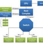
As an engineer I learn new concepts best by seeing a demonstration, in this case it was a demo of how to optimize SoC performance by using an ASIC prototyping debug process. SoC designers that use FPGAs to prototype their new ASIC often encounter debug issues, like:
- Limited observability of internal nets required for debug, maybe only 1,000 nets for 1,000 clock cycles
- Adding new internal probes requires a re-run of logic synthesis, causing delays of 8 or more hours
- Partitioning RTL to fit into FPGAs automatically or manually can be error prone, or non-optimal
The demo on YouTube comes from the embedded instrumentation group at Tektronixand shows how their technology adds observability into your FPGA prototype that remove the three debug bottlenecks listed above. The product name for this technology is called Certus, and with it you can:
[LIST=1]
Demo Steps
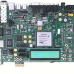
An FPGA prototype was created using the Xilinx ML509 development board, and contains:
- A 32 bit microprocessor, the SPARC V8
- Ethernet MAC
- JTAG port
- Compact Flash
- AMBA bus
- DDR2 DRAM Controller, 256 MB of DRAM
- SVGA output
- Serial ports for keyboard and mouse
- UART
- LCD controller
- PROM controller
Performance Optimization
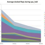
The system level goal was to minimize the round trip time from issuing a Ping command, to when packets are received.
To start this optimization a ping command is issued which starts the Ethernet traffic, and the connected router triggers the condition that we specified. Certus Analyzer captures about 6 seconds of realtime data from our SoC (millions of clock cycles), then presents it as VCD waveforms. Zooming into the waveform viewer we can see the trigger condition where the cursor points to the red line, and validate that the trigger address we requested is displayed as well:
System-level values like the latency between transmit packet and receive packet can be debugged in great detail, allowing measurements down to each clock edge. With this type of debugging you can now start to optimize your SoC to reduce latency because you can fully see all RTL signals and see from the waveforms what the bottlenecks are in the system.
Debugging State Machines
Now that we know more about our Ethernet MAC signals, we next focus our attention to a new set of signals, like the state machine signals. With just a few clicks in Certus Analyzer you can change the group of signals and in a few seconds start to analyze state machine signals for the Receive FSM:
Selected signals can be grouped together into a configuration, and for this design there were four configuration groups. You can quickly jump to a new configuration and immediately debug:
The CPU Pipeline stage configuration is selected, and we trigger when the state goes to run:
Summary
ASIC prototyping with FPGA devices is a great way to debug your new SoC design and then optimize the hardware and software. The SoC debug process can be significantly improved if you have full RTL-level visibility with millions of clock cycles and can correlate across multiple clock domains and FPGAs. The Certus technology from Tektronix is unlike anything else out there.
DAC
To see Certus at DAC visit Booth #819, or for more info send an email to EIG-info@tektronix.com
lang: en_US