DAC 2013 is closing in fast now…and if you haven’t made your plans for what you want to see and do, you’d better get going! Of course, I’m happy to help you out with a few suggestions…starting with that most important objective—conference swag. Stop by the Mentor Graphics booth (#2046, for those of you who actually look at your floor maps) any time Monday through Wednesday to pick up your plush Congress Bridge bat. And if you get the chance, go out one night and watch the real thing (take your camera!).
For those who like a bit of anticipation, we also have daily drawings. Prizes this year include an Apple iPad[SUP]®[/SUP]Mini, a Nintendo Wii U™, and a GoPro[SUP]®[/SUP]camera. You get an entry for every Mentor suite session you attend, and drawings will be held every day at our Happy Hour open bar, which starts at 4:00 pm. You don’t have to be present to win, but you must pick up your prize in person before the close of DAC.
If a lively bit of discussion is your thing, Mentor is participating in or hosting a number of panels at DAC. Join us for any or all. No advance registration is required.
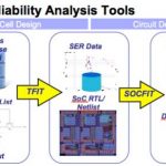
Achieving IC Reliability in High Growth Markets
Monday, June 3, 3:00-4:00 (Mentor Booth #2046)
Will Data Explosion Blow Up the Design Flow?
Monday, June 3, 3:15-4:00 (DAC Pavilion Panel, Booth #509)
Advanced Node Reliability: Are We in Trouble?
Tuesday, June 4, 10:30-12:00 (DAC Technical Panel, Room 16AB) requires full conference access
Marrying More than Moore
Tuesday, June 4, 3:00-4:00 (Mentor Booth #2046)
No Fear of FinFET
Wednesday, June 5, 3:00-4:00 (Mentor Booth #2046)
It’s also worth noting that the Mentor Booth panels are followed immediately by the Mentor Happy Hour—great chance to mingle with like minds, while enjoying an adult beverage!
As for those suite sessions—as usual, we’ll be hosting a variety of presentations at the Mentor booth. Below are just a few that might appeal to the Design to Silicon crowd, but you can check out the full list any time. Registration is required to attend a suite session—click on the session title to get to our registration page.
Reliability Checks for Multiple Markets(Presented in Mandarin)
Monday, June 3, 10:00-11:00, Mentor booth #2046
你說中文嗎? 你说中文吗? Calibre PERC provides a fully automated and comprehensive EDA design platform to check ESD, latch-up, EOS, ERC and other design issues in both design and stream out databases. In this session, presented in Mandarin, Mentor Graphics and SMIC discuss reliability checking with Calibre PERC. Want to hear it in English? Sign up for one of the Comprehensive Circuit Reliability with Calibre PERC sessions (Monday, 2:00 or Wednesday, 10:00) in the Mentor booth.
Best Practices for 20nm Design
Monday, June 3, 2:00-3:00, Mentor booth #2046
If you’re planning or contemplating a move to 20nm, you need to be in the seats for this session. TSMC and Mentor present best practices learned from their experience helping leading-edge customers with the transition to 20nm. This vital knowledge will help you smoothly tapeout your designs for TSMC’s advanced processes.
Advancing Circuit Reliability at TowerJazz with Calibre PERC Rule Decks
Tuesday, June 4, 2:00-3:00, Mentor booth #2046
Intended for advanced Calibre users, this presentation demonstrates how TowerJazz uses Calibre PERC rule decks and the Calibre PERC product’s unique ability to combine schematic (netlist) and physical layout information to perform circuit reliability verification during signoff. ONE TIME ONLY, LIMITED SEATING.
Preparing for Pervasive Photonics
Tuesday, June 4, 2:00-3:00, Mentor booth #2046
Silicon photonics is coming—are you ready? This session discusses the impact photonics will have on today’s IC design and manufacturing processes, the tool requirements for SP, foundry options, new applications that SP will open up, and new challenges it will present to IC designers.
Of course, we won’t just be hanging out at the Mentor booth the whole time. Calibre experts will be speaking at our partners’ booths as well. We have a full list of partner activities, but here’s one technical presentation you won’t want to miss:
Identifying Critical Design Features from Silicon Results
Tuesday, June 4, 10:00-11:00, GLOBALFOUNDRIES Booth #1314
Ken Amstutz (Senior Application Engineer) will be talking about the collaboration between Mentor Graphics and GLOBALFOUNDRIES to rapidly identify systematic defects and critical design features based on silicon data. Layout-aware diagnosis identifies the location and classification of defects causing manufacturing test failures. Specialized statistical analysis coupled with design profiling data (such as critical feature analysis) then determines the root cause of yield loss and separates design- and process-induced defects. LIMITED SEATING – REGISTRATION REQUIRED
For a full round-up of Mentor activities at DAC, and to register for any of our suite sessions in advance, you can check us out at Mentor@DAC 2013. See you in Austin!!