Through my contacts at SemiWiki I was introduced to a mixed signal IP company named SilabTech, and then decided to interview the founder and CEO, Sujoy Chakravarty.
Sujoy Chakravarty, CEO and Founder
Continue reading “AMS IC Design at SilabTech”


Through my contacts at SemiWiki I was introduced to a mixed signal IP company named SilabTech, and then decided to interview the founder and CEO, Sujoy Chakravarty.
Sujoy Chakravarty, CEO and Founder
Continue reading “AMS IC Design at SilabTech”

A SemiWiki member mentioned CircuitLaba few months back so I took a look at it today and share my first impressions.
At the onset of SoCs with multiple functionalities being packed together at the helm of technologies to improve upon performance and area; power, which was earlier neglected, has become critical and needs special attention in designing SoCs. And there comes reliability considerations as well due to multiple electrical and physical effects coming into existence at lower nodes and high density of SoCs. Both, power and reliability of chips need specific focus to analyze and fix issues at the earliest in the design phase.
I was all ears to a webinar presented by N. Kannan of Freescale Semiconductorwho talked in great detail about how they are tackling the challenges of power and reliability in their advanced automotive and networking SoCs; and also on how they are leveraging Apachetools like RedHawk[SUP]TM[/SUP], Totem[SUP]TM[/SUP], CPM[SUP]TM[/SUP], PathFinder[SUP]TM[/SUP], PowerArtist[SUP]TM[/SUP], Sentinel[SUP]TM[/SUP]and others for these purposes. It extremely impressed me knowing about various capabilities of these tools and prudence being exercised at Freescale in designing SoCs. It’s my pleasure to introduce below just a glimpse of those.
Automotive SoCs typically have on-chip Flash, Power Management Unit (PMU) and Analog IPs with multi-power domain and require PCB-Package-Die sign-off for electromagnetic compliance. Networking SoCs, on the other hand, have very large design sizes with multiple cores running at high frequencies, thereby requiring high peak and average power consumption. Package-Die sign-off for power integrity, signal integrity, simultaneous switching output and thermal conduction is a must for these SoCs.
RedHawk[SUP]TM[/SUP]is used for electrical as well as physical modelling. In case of standard cells, modelling of current and capacitance can be done by using Apache Power Library (APL) format. Current de-rating due to voltage drop is captured in the model. In case of Multi-Bit Flops, RedHawk[SUP]TM[/SUP]simplifies the modelling by approximation to the tune of just n characterizations for an n-bit flop. In case of a memory, RedHawk[SUP]TM[/SUP] is able to recognize bit-cell array regions inside the memory and provide more accurate distribution of currents and capacitances.
[Electrical Modelling Options]
Depending on size and nature of the design any or all of these three options can be used for electrical modelling. Option-1 is very simplistic model based on approximation; option-2 is most commonly used where full simulation data is used and option-3 is most expensive on run time where transistor level modelling is done using Totem[SUP]TM[/SUP]. This provides full simulation based analysis and is used in cases such as Flash where uniform current distribution is required.
RedHawk[SUP]TM[/SUP] provides extensive checks for connectivity and reliability such as weak spots in the grid, resistance bottlenecks (through short path tracing), missing vias, EM violations, IR drop bottlenecks, current hot-spots and so on; and provides what-if scenario analysis on IR and EM by using region based power assignment.
As an example, a long wire high resistance is pointed out during PG weakness check and a PAD consuming very high current during PAD placement quality check. PAD placement needs to be optimized with respect to average current ratio.
Similarly, clock buffers may be clustered in a particular region, leading to high switching and power density there, which needs to be fixed.
EM violations in regions of high current sourcing such as PAD locations and hot-spots due to excessive dynamic IR drop in regions with high activity logic clustering need fixes.
CPM[SUP]TM[/SUP](Chip Power Model) is used to do compact abstraction of full chip Power Distribution Network (PDN). Chip, package or board level simulation can be done. Frequency spectrum of chip current demand can be obtained. Time domain analysis can be done for the chip-package. High frequency noise associated with high peak current and corresponding layout regions can be identified and corrected for EM compliance.
Kannan also talks about reliability sign-off done by using Totem[SUP]TM[/SUP]on standard cells. They are also working on using PathFinder[SUP]TM[/SUP]for ESD and current density checks and PowerArtist[SUP]TM[/SUP]for RTL power estimation and reduction. They are working with Sentinel[SUP]TM[/SUP] for Chip Power density and Thermal Map analysis.
The actual delivery of the webinar is very exhaustive, containing details about various problems and the ways to fix them. This presentation was also done in DAC2013. Thanks to Apache and Freescale for making it freely available for our larger community. The webinar, titled “Power, Noise and Reliability Consideration for Advanced Automotive and Networking ICs” can be found here.

The US Executive Forum hosted by the Global Semiconductor Alliance is coming up on September 25th at the beautiful Rosewood Sand Hill Hotel in Menlo Park. Over 150 executives from the semiconductor and technology industry will attend creating a truly unique opportunity to listen to some of the world’s foremost speakers address topics such as US competitiveness and innovation. More importantly, you get the opportunity to meet the attendees themselves. Take a look at this LIST! CEOs, CTOs, the Who’s Who of the semiconductor industry ready to meet and greet you at the VIP reception.
As if that isn’t enough, the keynote speaker is Dr. Condoleezza Rice. She served as the 66th United States Secretary of State and is currently a faculty member of the Stanford Graduate School of Business and a director of its Global Center for Business and the Economy. Dr. Rice will share her unparalleled expertise on how America’s policies influence international trade relations and global affairs. Following her keynote address, Dr. Rice will engage the audience in an interactive Q&A session.
Clearly WHO you know in this business is as important as WHAT you know so do not miss this opportunity to expand your horizons. GSA is the unifying body of the global semiconductor industry. Membership spans the entire ecosystem, representing the world’s best IDMs, fabless companies, and their suppliers. If your company is not a member it should be.
[TABLE] cellpadding=”5″ style=”width: 100%”
|-
| style=”width: 149px” | Time
| style=”width: 1218px” | Activity
|
|-
| valign=”top” | 12:00 p.m.
| Networking Lunch
| style=”width: 35px” |
|-
| valign=”top” | 12:45 p.m.
| Opening Remarks
|
|-
| colspan=”3″ align=”center” valign=”top” | Connected Services in the Digital Era
|-
| valign=”top” | 1:00 p.m
| Keynote Address
This Keynote Address will capture the technological landscape in the next decade and discuss its impact on consumers’ lives.
David Small, Chief Platform Officer, Verizon Enterprise Solutions
|
|-
| valign=”top” | 1:30 p.m.
| Panel Discussion
This Panel Discussion will address game-changing trends stemming from the Internet boom, with a focus on superior content delivery via today’s burgeoning network and appliances.
|
|-
| valign=”top” |
| Panelists:
|
|-
| valign=”top” |
|
|
|-
| valign=”top” |
|
|
|-
| valign=”top” |
|
|
|-
| valign=”top” | 2:30 p.m.
| Networking Break
|
|-
| colspan=”3″ align=”center” valign=”top” | Championing Economic Growth
|-
| valign=”top” | 3:00 p.m.
| Keynote Address
This Keynote Address will unveil insight on enabling private sector growth, innovation and competitiveness amid today’s political and economic landscape.
|
|-
| valign=”top” | 3:30 p.m.
| Panel Discussion
This Panel Discussion will spotlight CEOs from leading semiconductor companies as they discuss amongst other things, the toughest challenges facing our industry today and what reforms can be made to address those challenges.
Moderator: Dr. Aart de Geus, Chairman & Co-CEO, Synopsys
Panelists:
|
|-
| valign=”top” |
|
|
|-
| valign=”top” |
|
|
|-
| valign=”top” |
|
|
|-
| valign=”top” |
|
|
|-
| valign=”top” | 4:30 p.m.
| Networking Break
|
|-
| valign=”top” | 5:00 p.m.
| Keynote Address and Interactive Q&A with Dr. Condoleezza Rice, Secretary of State (2005-2009)
Widely considered as one of the most influential and powerful people in the world, Dr. Condoleezza Rice will share her unparalleled expertise on how America’s policies influence international trade relations and global affairs. Following her keynote address, Dr. Rice will engage the audience in an interactive Q&A session.
| valign=”top” |
|-
| valign=”top” | 6:00 p.m.
| Closing Remarks and Reception
|
|-
Have questions about this Forum? Please contact:
Nicole Bowman
O 972.866.7579 ext. 129
M 972.814.6866
E nbowman@gsaglobal.org
lang: en_US
If you are my age, you know that the most influential book in that era on VLSI design was Carver Mead and Lynn Conway’s textbook, blah VLSI blah. Nobody can remember exactly what its title was, it was just referred to as Mead and Conway. In my opinion it was the most influential book on semiconductor design ever. It opened up VLSI design to computer scientists, and since they understood complexity they eventually won out over the EE guys as designs got insanely complicated…10,000 gates, how can we cope?
Lots of us (and even you youngsters who came later) owe a lot to Mead & Conway. So who were they? Carver Mead was a professor at CalTech and Lynn Conway was a researcher at Xerox PARC (Palo Alto Research something-beginning-with-C probably Center). But Lynn Conway had a deep secret that in those days she wasn’t ready to reveal.
She started life as a guy.
S/he had a hugely successful research career as a young researcher at IBM on supercomputing stuff that even today is part of the techniques in the most modern microprocessors, basically the foundations of out-of-order execution. But she was a woman trapped in a man’s body and eventually she decided she had to do the whole thing and do gender reassignment surgery. This was too much for IBM at the time (and let me be the first to point out that today’s IBM would never do this) so they fired him/her. She is private about what her real name was back then to protect lots of people from her family to her then-friends, and uses the name Robert Sanders for that period of her life.
So she was basically screwed, with no family, friends or job. She got some positions as a contract programmer. OK, let’s face it, she was an incredibly good contract programmer. But how do you get from A to B.
The guys at PARC, which was just starting up, noticed her at Memorex, where she was working, and recruited her. PARC in that era was the most innovative computer science location in the world, blowing away Bell Labs and places like that, as well as every academic department from Stanford to MIT. A huge proportion of the top computer scientists in the world worked there. Including Lynn Conway.
I met her last summer at a party for the first time, at Dick Lyon’s house (inventor of the first optical mouse) although we’d exchanged a few emails.
This June, Lynn went to the White House to celebrate LBGT pride month. I live in San Francisco so this is a big deal here every year. But Lynn’s story is something even more of a big deal. The guys at PARC recruited her. Think how different the world might have been if that had not happened. Moore’s law would have advanced and presumably someone else would have tamed the complexity in some way. But Carver Mead and Lynn Conway were just in the right place at the right time to lead people like me into what became the VLSI world.
Lynn’s reminiscences here. Huffpost article by Lynn from last week here.

RTL coding using languages like Verilog and VHDL have been around since the 1980’s and for almost as long a time we’ve been hearing about High Level Synthesis, or HLS that allows an SoC designer to code above the RTL level where you code at the algorithm level. The most popular HLS languages today are C, C++ and SystemC. Several EDA vendors have tools in this space, and one of them is Forte Design Systems, founded in 1998.
My question today is, “What applications implement best with HLS?”
Let’s take a look at three application categories that make sense to use an HLS approach.
Digital Media
I love to view or create digital media with my devices:
Each new generation of graphics processing in a tablet is increasing throughput by about 4X, creating smoother experiences. With all of the increase in pixel counts and frame rates, designers must still meet more competitive battery life times which means controlling power throughout the design process.
Hardware acceleration of algorithms is the way to make your consumer devices stand out, instead of using software-based approaches on a general purpose CPU.
If you insist on coding at the RTL level it will simply take you much longer to explore, refine and implement a given algorithm. For example an IC designer coded a motion estimator block using C code in just 1/4th the time compared with using RTL code.
Digital media designers can code in C their algorithms directly:
Security
I’ve done some web programming where sensitive credit card data needed to be encrypted and decrypted so I used a PHP function for the MD5 algorithm. Likewise, an SoC can have this same algorithm in hardware
Here’s a list of security algorithms well suited for HLS:
To get a feel for what the SystemC code looks like for any of these algorithms visit the OpenCores web site which also shows the same code in Verilog.
Wireless
The final application area well suited to use HLS is wireless, driven by consumer electronics devices and the IoT (Internet of Things). Instead of coding in RTL and then getting surprised when the specification changes which can add weeks to your SoC schedule, you can code at the algorithm level and update your code then re-synthesize in days or hours.
Examples of wireless applications include:
Summary
HLS is here to stay and there’s a growing list of applications that will benefit from coding algorithms in SystemC. Forte offers an HLS tool called Cynthesizer that is well-used in the industry for Digital Media, Security and Wireless applications.
lang: en_US

At Semicon I met with Applied Materials to learn about epitaxy. This is when a monocrystalline film is grown on the substrate which takes on a lattice structure that matches the substrate. It forms a high purity starting point for building a transistor and is also the basis of the strain engineering in a modern process.
Since holes have lower mobility than electrons, p-type transistors are inherently lower performance than n-mos transistors (which is why before we had CMOS, semiconductor was dominated by NMOS and its variants, n-type transistors with some sort of pull-up resistor/transistor). Since epitaxy improves performance, it was first used for the p-type transistors.
Basically, the source and drain are etched out to form a pit and then the pit is filled by depositing epitaxial silicon (with Applied Materials equipment in most cases). It is actually deposited until the source/drain is proud of the surrounding silicon. Adding small amounts of impurities that are larger than silicon, such as germanium, during deposition induces strain in the lattice which turns out to enhance mobility in the channel. It increases transistor speed but does so, unlike many other things we might do, without increasing leakage and so without increasing static power.
But now, at 22/20nm nodes, epitaxy is needed to get extra performance out of the n-type transistors too, an contribution of around 20% of the mobility.
As usual, almost anything associated with p-type transistors is the other way around for n-type. So to improve performance, strain needs to be tensile. To induce tensile strain in n-type transistors the impurities need to be smaller than silicon, such as carbon or phosphorous atoms. Carbon is 62% smaller than a silicon atom, for example. This increases electron mobility and thus n-type transistor performance.
There are several advantages of epitaxy especially when it is used for both transistor types:
Applied are the leader in equipment for epitaxy having shipped over 500 systems (and more every week). Their revenue in this area increased by 80% over the last 5 years. Looking forward, the market is moving towards new channel materials such as III-V elements which have inherently higher electron mobility.
The bottom line message: nMOS epitaxy is essential for faster transistors inside next-generation mobile processors. It boosts transistor speed by the equivalent of have a device node without increasing off-state power consumption. What’s not to like? That is why it is coming to a 20/22nm process near you.
More details here.
How reliable is your cell-phone? Actually, you don’t really care. It will crash from time to time due to software bugs and you’ll throw it away after two or three years. If a few phones also crash due to stray neutrons from outer space or stray alpha particles from the solder balls used in the flip-chip bonding then nobody cares.
How about your heart pacemaker? Or the braking system in your car? Or the router at the head of a transpacfic fiber-optic cable? OK, now you start to care.
iRocTech provides audit services at the system level for these sort of situations. However, at the system level, the overall reliability depends, obviously, on the reliability of the various components. One big problem is that the component suppliers are not always co-operative. In some cases they simply don’t know the reliability of their components. But also they tend to want to provide the best possible data so that it cannot be used against them. It is as if we went to TSMC and asked about cell-timing and got given the typical corner and then were told that they hadn’t a clue when we asked about a worst case corner because they didn’t want anyone to know just how slow the process might get.
The problem is actually getting worse. For all the same reasons that we want to put 28nm and 20nm silicon into cell-phones (especially low dynamic and low leakage power, lots of gates, performance), engineers designing implantable medical electronics and aviation electronics want to do so to. But the leading edge processes and foundries are driven by the mobile industry which is probably the industry the least concerned with reliability of all semiconductor end-markets (well, OK, birthday cards that play a tune when you open them, $5 calculators, but these are not really markets). This means that there is not as much focus on reliability and measuring it as the markets outside of mobile require.
The big markets that iRoC works on for system reliability are:
What these industries would like to do is to push down their system reliability requirements to the component vendors, but compared to mobile they don’t have enough influence, at least in the short term. A second best solution is to find out the reliability of the components and back it up to a system reliability number.
One end-market that is not on the list is cloud computing. At the level of big data centers, events that we consider rare on our own computer (a disk drive fails, the processor melts, the power-supply blows up) are everyday occurrences and so the infrastructure has to be built to accommodate this. For example, GFS (Google File System) never stores any file on less than three separate disks in different geographical locations (Google is actually prepared for a meteor hit on a datacenter that permanently destroys it without impacting service). I don’t want to imply Google is special, I’m sure Facebook and Amazon and Apple are all the same, just that I know a little more about Google since they have published more in the open literature (and I have done some consulting for them).
Since some measurable problems especially latchup and single event failure interrupt (SEFI) are actually very rare, they are hard to measure. If only a short period of measurement is done then the numbers may look deceptively good. However, the reality is that the mean might be good but the standard deviation is enormous. A better reliability measure than the mean alone is the mean plus one standard deviation. To get that measure to look good, extensive measurement is required to get the standard deviation down to something manageable along with a better estimate of the mean. Single event upsets (SEE) which can be accelerated with a neutron beam (as I wrote about here) are much more common and so the standard deviation is much narrower.
Of course, once there is a measure, the question is what to do about it. It is a well-known proverb that a chain is only as strong as the weakest link. But a corollary is that there is no point in having especially strong links, in particular there is no point in strengthening links other than the weakest. Identifying the lowest reliability component and improving it is how overall system reliability can be improved.
iRoc Technologies website is here.

This week, I had a nice opportunity meeting Charu Puri, Corporate Marketing and Sushil Gupta, V.P. & Managing Director at Atrenta, Noida. Well, I know Sushil since 1990s; in fact, he was my manager at one point of time during my job earlier than Cadence. He leads this large R&D development centre, consisting about 200 people at Atrenta’s Noida facility. In fact, they have just moved into a new building, yet to be inaugurated. I will write more about it and various development stories when the inauguration happens.
[Sushil Gupta]
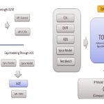
Coming back to Atrenta’s product and technology edge; it was an intriguing discussion on how Atrenta is solving today’s SoC problems. Sushil talked about Atrenta’s SpyGlass being deployed for SoC designs across the complete mobile ecosystem; rightly, as what we have on a PC or laptop today has shifted to the handheld smart phone. And that has been possible with the advent of SoCs where multiple functionalities have been squeezed into the same chip. However it’s not so simple a road to ride as there are tremendous challenges considering the very small window of opportunity for a design, the complexities of verifying and integrating multiple blocks and IPs from different origins, process bottlenecks and physical effects at small geometries, performance-power-area optimization and so on. The only viable option is to reduce long iterative loops in the design flow and introduce shorter and faster loops, early in the cycle, to set the design right. That would significantly reduce the possibility of re-spins and also provide an edge for time-to-market.
So, there comes Atrenta’s philosophy of pulling up the sign-off process at the earliest possible opportunity, i.e. at the register transfer level (RTL). Well, that cannot completely eliminate layout sign-off, however can definitely and significantly reduce long iterative loops from layout to earlier stages and enable the designer to achieve faster convergence of the design. Traditionally, sign-off is done at the last stage prior to fab, i.e. layout.
As is evident, post layout sign-off is too late and too risky.
Atrenta’s guiding methodology is to do RTL sign-off before proceeding further. And Atrenta provides a complete platform for RTL sign-off. That’s amazing!!
As we can see, the platform contains all the ingredients to realise an SoC that includes a complete design flow, IP flow and integration, debug and optimization. In fact, Atrenta has also collaborated with TSMCand provides an IP Kit which validates and qualifies any soft IP as per TSMC process before they are integrated into SoCs.
I will talk more about Atrenta’s individual products/technologies and their capabilities in my future articles. But I must share my remembrance that when I had a first read (about two years ago) of the Atrenta SoC Realization whitepaper, I had talked about it with Sushil in his earlier office. And today, to my excitement, Atrenta has really further strengthened that realization!!

For those taking a quick look at the various MIPI Interface specification, the first reaction is to realize that they will have to look at MIPI more closely, and that it will take them longer than expected to make sure they really understand the various specifications! Let’s start with the PHY. One specification defines the D-PHY, up to 1 Gbps (1.5 Gbps is also defined, but not really used), another defines the M-PHY, to support higher data bandwidth and higher speed. Look simple? In fact, we did not mention the various “gear” supported by M-PHY (per lane): Gear 1 is up to 1.25 Gbps, Gear 2 up to 2.5 Gbps when gear 3 is defined up to 5 Gbps. In fact there are many more differences between D-PHY and M-PHY, if you take a look at MIPI Org web site, you will find this comprehensive picture:
Now, you clearly understand the various MIPI PHY, and you know that a PHY is nothing without a Controller, the digital part of the function in charge of processing the protocol layers, like “Link Layer”, “Transport Layer” and so on. Let’s stay with the M-PHY example. If life would be simple, you would attach one MIPI Controller to this M-PHY. But, if we are (more or less) well paid engineers, it’s because SC related life is not simple… Just take a look at the picture below:
In order to ease SoC integration, M-PHY can support up to six different protocols. This means that when a chip maker decides to integrate several MIPI protocols on the same chip, he wills also instantiates several times the same PHY IP, and the various controllers attached. All controllers are not made equal: DigRF (interfacing with RF chip), LLI (interfacing the SoC and a modem chip, to share a unique DRAM) and SSIC (SuperSpeed USB IC protocol, for board level inter-chip connection) can be plugged directly with the M-PHY. But, another group of Controllers (CSI-3, DSI-2 and UFS) require another piece of IP, UniPro, to be inserted between M-PHY and, for example, MIPI CSI-3 controller (Camera Serial Interface specification).
When a chip maker designs an Application Processor for smartphone or media tablet, he is integrating over 100 IP, from ARM A9 to I2C or SRAM. Such a chip maker will certainly appreciate the fact that Synopsys propose a complete Camera Serial Interface 3 (CSI-3) host solution, including the new DesignWare MIPI CSI-3 Host Controller IP combined with the MIPI UniPro Controller and multi-gear MIPI M-PHY IP. With support for up to four lanes in Gear1 to HS-Gear3 operation, the CSI-3 host solution simplifies the system-on-chip (SoC) interface for a wide range of image sensor applications, giving SoC designers maximum flexibility to increase throughput while reducing pin count requirements and integration risk.
I agree with Joel Huloux, MIPI Alliance Chairman when he says: “IP supporting the MIPI CSI-3 v1.0 specification, along with a HS-Gear3 M-PHY, gives designers the ability to rapidly build host configurations into their SoCs,”. “Synopsys’ DesignWare MIPI CSI-3 Host Controller promotes the MIPI ecosystem while furthering the realization and reach of the latest MIPI specifications.” Working in the IP business for about 10 years, I have realized how important it is for a chip maker who decides to outsource a certain function, split into PHY and Controller, to have the opportunity to acquire a complete solution with a single supplier. This is the guarantee that the function has already been integrated (by the vendor), and also validated and verified before he will integrate it. In this case of a Camera solution, we are talking about three different functions! Last but not least, this new MIPI CSI-3 Host Controller, simplifying CSI-3 image sensor interface integration, is a low power solution.
By Eric Esteve from IPNEST
lang: en_US