Hierarchical IC design has been around since the dawn of electronics, and every SoC design today will use hierarchy for both the physical and logical descriptions. During the physical implementation of an SoC you will likely run into EDA tool limits that require a re-structure of the hierarchy. This re-partitioning will cause a change to the logical hierarchy and require some functional verification re-runs.
Kathryn Kranen Wins UBM Lifetime Achievement Award 2013
UBM’s EETimes and EDN today announced Kathryn Kranen as the lifetime achievement award winner for this years ACE awards program. Kathryn, of course, is the CEO of Jasper (and is also currently the chairman of EDAC). Past winners exemplify the prestige and significance of the award. Since 2005 the award was given to Gordon Moore, then the Chairman emeritus of Intel, Wilf Corrigan, the Chairman of the board of LSI, Chung-Mou Chang the Founding Chairman of TSMC and Pasquale Pistorio the honorary Chairman of ST.
As CEO of Jasper, Kathryn has taken Jasper’s formal approaches to verification from a niche to a mainstream tool, managed to raise a round of funding in a very difficult environment, and put Jasper on the path to success.
Prior to Jasper, Kathryn was CEO of Verisity. While serving as CEO of Verisity Design, Kathryn and the team she built created an entirely new market in design verification. (Verisity later became a public company, and was the top-performing IPO of 2001, and subsequently was acquired by Cadence).
Prior to Verisity, Kathryn was vice president of North American sales at Quickturn Systems. She started her career as a design engineer at Rockwell International, and later joined Daisy Systems, an early EDA company. In 2009, Kathryn was named one of the EE Times’ Top 10 Women in Microelectronics. In 2012, she became a member of the board of trustees of the World Affairs Council or Northern California. She is currently serving her sixth term on the EDA Consortium board of directors, and was elected its chairperson in 2012. In 2005, Kathryn was recipient of the prestigious Marie R. Pistilli Women in Electronic Design Automation (EDA) Achievement Award. She graduated summa cum laude from Texas A&M University with a B.S. in Electrical Engineering.
You may know that over on the DAC websitewe are running a “my DAC moment” series of stories. Kathryn has set the bar so high that it is hard to beat. She got engaged at DAC. Here is her story:My favorite DAC memory: Las Vegas in 1996. I was working for Quickturn at the time, and my now-husband Kevin worked for Synopsys. On the Wednesday morning of DAC, Kevin “popped the question”, and I eagerly accepted his proposal. We then both rushed off to our various DAC meetings.
I was mesmerized by my diamond engagement ring, sparkling under the huge lights in the exhibit hall. It was great fun to share our happy news with hundreds of EDA friends and co-workers. That evening, some friends and Kevin and I looked for an Elvis wedding chapel, thinking a fake wedding photo would be a fun way to spring the engagement news on our parents. Alas, all the Elvis wedding chapels were booked *on a Wednesday!
Cell Level Reliability
I blogged last month about single event effects (SEE) where a semiconductor chip behaves incorrectly due to being hit by an ion or a neutron. Since we live on a radioactive planet and are bombarded by cosmic rays from space, this is a real problem, and it is getting worse at each process node. But just how big of a problem is it?
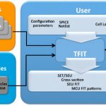
TFIT is a tool for evaluating all the cells in a cell-library, or the cells in a memory (or memory compiler) to calculate just how vulnerable they are to SEE causing a failure-in-time (FIT). It is very fast and the test results are within 15% for any type of cells. Within 15% of what? Within 15% of the actual value, which is determined by going to Los Alamos and putting real chips in a beam of neutrons so that damage is accelerated (or similar tests with alpha particles). IROC provide this as a service, btw, but that is a topic for another blog.
Since manufacturing silicon and bombarding it while designing a cell-library is not practical, TFIT is the way to get a “heat map” of where cells are vulnerable, in just the same way as we use circuit simulation to characterize the timing performance of the cells without having to manufacture them. Vulnerable transistors in the flop above, for example, are highlighted. The color corresponds to different linear energy transfer (LET) values. High energy particles only need to hit anywhere in the outer black rings, but, as you would intuitively expect, lower energy particles have to hit more directly as shown in red.
TFIT takes as input process response models (which today usually comes directly from the foundry since foundry A doesn’t really want foundry B analyzing their reliability data in detail). These are available for most recent processes in production at both TSMC and Global plus more generic models for older processes at 180nm, 90nm and 65nm. Along with that is iROC’s secondary particles nuclear database. The cell requires both layout and a spice netlist.
Memory analysis is a bit more complex since the bit cells are so small that a single particle can impact multiple bits, known as a multi-cell upset (MCU). The reliability data can then be used to decide on appropriate error correcting codes and how to organize the bits. Again, results are within 15%.
The tool can be run interactively on a single cell but it is often used in batch mode to characterize the vulnerability of an entire cell library. To analyze a single impact on an SRAM cell takes just a few seconds. The only comparable way to do analysis is to use TCAD which takes 4-8 hours. For more detail, which requires analyzing more than a single impact or a whole library, the TCAD approach is just not practical.
Rare earth syndrome: PHY IP analogy
If you ask to IP vendors selling functions, PHY or Controller, supporting Interface based protocols which part is the master piece, the controller IP only vendors will answer: certainly my digital block, look how complex it has to be to support the transport and logical part of the protocol! Just think about the PCI Express gen-3 specification, counting over 1000 pages… Obviously, the PHY IP vendor will claim to procure the essential piece: if the PHY does not work 100% according with the specification, nothing works! Now, would you ask me to answer this question, I will reply… by a question: do you know anything about the rare earth element case?
Rare earth metals are a set of seventeen chemical elements in the periodic table, specifically the fifteen lanthanides plus scandium and yttrium, which are used, even in very tiny amount, in almost every electronic systems, and most certainly in advanced systems, from iPhone to catalytic converters, from energy efficient lighting to weapons systems, and many more. To make a long story short, for short term consideration (I mean stock market dictated view, where the long term is the end of the fiscal year), rare earth extraction and sales are at 95% concentrated into a single country, when every high tech industry need to access it.
Hopefully, nothing similar has happened with the PHY, except that it’s an essential piece of modern semiconductor industry, and like CPU or DSP IP core, and that you find it in most of the ASIC and ASSP, providing the chip has to communicate through a protocol (PCIe, MIPI, USB, SATA, HDMI, etc.) or address an external DRAM at data rate over 1 Gb/s. By the way, I have answered your question: to me, the PHY IP is the master piece of the protocol based function. Developing high speed digital controller certainly require talented design architect, able to read and really understand the protocol specification, then to manage a digital design team implementing the function, and interfacing with a Verification team in charge of running the VIP to check for protocol compliance. But at the end, if the design team was mediocre, the IP will probably still work at spec, even if the latency could be too long, or the area or the power larger than what was optimally possible to reach.
Because PHY design is still heavily based on mixed-signal design techniques, developing first time right function is a much more challenging task requiring highly experienced designers. Would you follow a mediocre design approach, this will lead to failing result: there are simply too many reasons why a design could fail. So, creating a PHY design team requires to find highly specialized design engineers, the type of engineers starting to do a decent job after five or ten years of practice, and being good after fifteen or twenty years’ experience! This is the reason why, even if you look all around the world, you will only find a handful (maybe two if you take into account the chip makers) of PHY design capable teams. That’s why I am happy to welcome Silab Tech, one of these talented PHY IP vendors!
The PHY IP market, during the last couple of years, has consolidated:
- Synopsys has acquired in 2012 MoSys PHY IP division (former Prism Circuit bought by MoSys in 2009),
- Gennum (parent company of Snowbush, well known PHY IP vendor) was acquired by Semtech at the end of 2011 and the company decided to keep Snowbush PHY for their internal use, or to address very niche market.
- VSemiconductor was developing Very High Speed PHY (up to 28 Gbps) for Intel foundry, finally Intel decided that it was even easier to buy the company, at the end of 2012.
- Very recently, Cadence bought Cosmic Circuits, another mixed-signal IP vendor also selling MIPI and USB 3.0 PHY.
Consolidation is the mark for mature market, but the PHY part of the Interface IP market still has a strong growth potential: the overall (PHY and Controller) IP market has weighted $300M in 2012, but it should pass $500M in 2016. Moreover, if the Interface IP market revenue sharing was 50/50 in 2008 between PHY and Controller in value, the PHY IP share has been above 60% in 2012 and the trend will go on this way! Welcoming a new PHY IP vendor is certainly good news for chip makers, a diversified offer allowing better flexibility, offering more design options when selecting optimum technology node for a specific circuit.
As I mentioned earlier in this paper, to start a successful PHY and analog IP vendor, you need to rely on a strong, talented and experienced design team. As we can see on the above chart, Silab Tech founders have acquired most of their experience when working for TI. TI is known to be an excellent company to develop engineering competency, it is also a company where technical knowledge is valued at the same level than managerial. When, in many companies, the only way to progress is to become a manager, a good technical engineer can get the same level of reward than a good manager when working for TI. That’s the reason why Silab Tech’s management team exhibit various domain of expertize like PLL, DPLL, High Speed serial interface or ESD…
By the way, these are precisely the area of expertize you need to develop high speed PHY IP, like this you can see in the picture labeled “PHY: 2 lanes example”, extracted from a Silab Tech test chip recently taped out. To create an efficient PHY IP design team, the managers need to rely on a strong experience, but this is also true for the design engineers, and this is the case with Silab Tech, where most of the engineers have long analog design background, similar to the management team. No doubt that Silab Tech name will become very popular for the chip makers involved in large SoC design, like was Snowbush in the early 2010’s. But the difference with Silab Tech is that they are in the IP business to stay, develop the company and serve their customers.
By Eric Esteve from IPnest
Phil Kaufman Award Recipient 2013: Chenming Hu
This year’s recipient of the Kaufman Award is Dr Chenming Hu. I can’t think of a more deserving recipient. He is the father of the FinFET transistor which is clearly the most revolutionary thing to come along in semiconductor for a long time. Of course he wasn’t working alone but he was the leader of the team at UC Berkeley that developed the key structures that keep power under control and so allow us to continue to scale process nodes.
In the past, the Kaufman Award recipient has been finalized in the summer and actually awarded at a special dinner in the fall. This year is different. The award will take place at DAC in Austin on Sunday evening. The award will be presented by Klaus Schuegraf, Group Vice President of EUV Product Development at Cymer, Inc.
A quick bio of Dr Hu:In a professional career spanning four decades, including over thirty years as a professor of electrical engineering and computer science at UC Berkeley, Dr. Hu has advanced semiconductor technologies through his nearly one thousand research publications including four books, led or helped build leading companies in the industry, and trained hundreds of graduate students. His students occupy leadership positions in industry and academia. Dr. Hu received a bachelor degree from National Taiwan University, masters and PhD degrees from UC Berkeley. He has served on the faculty of MIT and UC Berkeley as well as the chief technology officer for TSMC, the world’s largest semiconductor foundry. He founded Celestry Design Technologies, an EDA company that was later acquired by Cadence Design Systems. He was elected to the US National Academy of Engineering in 1997, the Academia Sinica in 2004, and the Chinese Academy of Sciences in 2007. He received the IEEE Andrew S. Grove Award, the Don Pederson Award and the Jun-Ichi Nishizawa Medal for his contributions to MOSFET device, technology and circuit design. Among his many other awards is UC Berkeley’s highest honor for teaching, the Berkeley Distinguished Teaching Award. Dr. Hu served as a board chairman of the nonprofit East Bay Chinese School and currently serves on the board of the nonprofit Friends of Children with Special Needs.
Often the Kaufman award is for work that had a major influence on EDA or semiconductor many years ago, although of course like Newton (Isaac, not Richard) almost said, today’s EDA stands on the shoulders of yesterday’s giants. Certainly Dr Hu’s work on device modeling has had that sort of effect. But it is hard to imagine a more timely award than this, nor to better what Aart de Geus, chairman of the award selection committee, said:
“Recognizing Chenming Hu the very year in which the entire EDA, IP, and Semiconductor industry is unleashing the next decade of IC design through the 16/14nm FinFET generation is not a coincidence, but illustrates how a great contributor can impact an entire industry!”
The full press release is on the EDAC website here.
TSMC to Talk About 10nm at Symposium Next Week
Given the compressed time between 20nm and 16nm, twelve months versus the industry average twenty four months, it is time to start talking about 10nm, absolutely. Next Tuesday is the 19th annual TSMC Technology Symposium keynoted of course by the Chairman, Dr. Morris Chang.
Join the 2013 TSMC Technology Symposium. Get the latest on:
- TSMC’s 20nm, 16nm, and below process development status including FinFet and advanced lithography insights
- TSMC’s new High-Speed Computing, Mobile Communications, and Connectivity & Storage technology development
- TSMC’s robust Specialty Technology portfolio that includes CMOS Image Sensor (CIS), Embedded Flash, Power IC and MEMS
- TSMC’s GIGAFAB™ programs and improvements that enhance time-to-volume
- TSMC’s 18-inch manufacturing technology development
- TSMC’s Advanced Backend Technology for 3D-IC, CoWoS (Chip-on-Wafer-on-Substrate), and BOT (Bump-on-Trace)
- New Design Enablement Flows and Design Services on TSMC’s Open Innovation Platform®
TSMC takes this opportunity each year to let customers know what is coming and get feedback on some of the challenges we will face in the coming process technologies. I remember 2 years ago when TSMC asked customers openly if they were ready for FinFETs. The answer was mixed, the mobile folks definitely said yes but the high performance people were not as excited. Here we are, two years later, with FinFET test chips taping out. So yes, these conferences are important. This is the purest form of collaboration and SemiWiki is happy to be part of it.
TSMC will also let us know that 20nm is not just on schedule but EARLY. They have been working around the clock to make sure our iPhone6s arrive on time so don’t expect any 20nm delays. In fact, recent news out of Hsinhcu says TSMC will begin installing 20nm production equipment in Fab 14 two months early of the June 2013 target. 20nm is also the metal fabric for 16nm FinFETs so expect no delays there either.
The COWOS update will be interesting. Liam Madden, Xilinx Vice President of FPGA development, did the keynote at the International Symposium on Physical Systems (ISPD) last month and three-dimensional integration was the focus on the kickoff day. EETimes did a nice write up on it: 3-D Integration Takes Spotlight at ISPD:
“For many years, designers kept digital-logic, -memory and analog functions on separate chips—each taking advantage of different process technologies,” said Madden. “On the other side are system-on-chip [SoC]solutions, which integrate all three functions on the same die. However now there is a third alternative that takes advantage of both worlds—namely 3-D stacking.”
3D transistors plus 3D IC integration will keep the fabless semiconductor moving forward at a rapid pace. If you would like to learn more, Ivo Bolsens, CTO of Xilinx, will be keynoting the Electronic Design Processing Symposium in Monterey, CA this month. The abstract of his keynote is HERE.
There is also a 3D IC panel “Are we there yet?” moderated by Mr 3D IC himself Herb Reiter. Herb will be joined by Dusan Petranovic of Mentor Graphics, Brandon Wang of Cadence, Mike Black of Micron, and Gene Jakubowski of E-System Design. Abstracts are HERE. Register today, room is limited!
Intelligent tools for complex low power verification
The burgeoning need of high density of electronic content on a single chip, thereby necessitating critical PPA (Power, Performance, Area) optimization, has pushed the technology node below 0.1 micron where static power becomes equally relevant as dynamic power. Moreover, multiple power rails run through the circuit at different voltages catering to analog as well as digital portions of the design. Pins in a gate can be driven by power rails at different voltages. IP blocks such as ARM micro-processors typically come with multiple power rails and also in-built power domains for power management of the blocks. The network according to its logical portions driven by particular supply nets is divided into different power domains, all of which may not be active at the same time. Any un-required domain can remain off hence saving the power. Various techniques and different types of multi-rail cells such as level shifters, power switches, isolation cells etc. are employed to manage power.
Tools must be capable of dealing with multiple power rails and intelligently associating logic with their respective supply nets. That would mean relating to the voltage levels at various nodes at which the design is operating. Also the connectivity and constraint between supply net and power pin, which depend on the context in which the multi-rail cell has been instantiated, needs to be captured. IPs can have separate internal power switches and logic divided into multiple power regions complicating the matter further.
Synopsys’s Eclypse Low Power Solution provides state-of-the-art verification tools MVSIM and MVRC and necessary infrastructure for complete low power verification. MVSIM accurately verifies all power transitions in succession through various voltage levels. MVRC statically checks for correct implementation of power management scheme. The system provides a comprehensive solution for verifying multi-rail cells at RTL, netlist and at PG-netlist stages of the design flow.
Eclypsecaptures cell level information such as logic to power pin association in Synopsys’s existing Liberty format enhanced with standard low power attributes thus providing consistent, integrated platform for the overall design flow enabling designers work independently at different levels such as chip, RTL or cell level in the flow. Chip level information such as chip-level power rail connection with cell-level power pins is provided in power intent file using UPF (Unified Power Format, IEEE 1801 standard). By using UPF a designer can define complete power architecture of the design; partition the design and assign blocks to various power domains which enable MVSIM and MVRC to infer power pin connections with associated logic. For hierarchical flow, Eclypse provides simple commands to associate inputs and outputs of a block to its power pins.
[Example – multi-rail design]
MVSIM accounts for right analog levels of voltages at various pins and hence can simulate different power techniques such as power gating, dynamic voltage scaling, state retention etc. For IPs it can detect available power-aware models and automatically replace the non-power-aware simulation models with the corresponding power-aware models. It also provides option to choose between power-aware or non-power-aware mode depending on the simulation requirement.
[MVSIM output of multi-rail design – with island_V3 off, instance3 output is corrupted]
MVRC verifies static power management of the design taking care of right connection between pins and their supply nets, right insertions and connections of low power structures like level shifters, power switches, retention registers etc. At RTL level, it combines the cell level information from the library with the chip level information available in the UPF format to determine the associated supply net for each node in the design and report any architectural issues or missing/redundant isolation/level-shifter policies in UPF. Similarly it can check netlist after synthesis or post layout for right power pin connectivity and missing/redundant cells with respect to policies defined in UPF.
A very nice detailed description about the methodology has been provided by Synopsys in its white paper located at Low Power Verification for Multi-rail Cells
Considering analog and digital designs to co-exist with increasing design size and complexity, operating at different voltage levels, it’s inevitable to go without multi-rails that introduce its own challenges to low power verification. Eclypse along with MVSIM and MVRC incrementally adds that extra intelligence into their system of library and chip level infrastructure including UPF to provide a comprehensive solution for static and dynamic power simulation and verification of multi-rail low power circuits.
What really means high reliability for OTP NVM?
Normal operation range for a Semiconductor device is not made equal for systems… If you consider a CPU running inside an aircraft engine control system, this device should operate at temperature ranged between -55°C and +125°C, when an Application Processor for smartphone is only required to operate in the 0°C to +70°C range. When Sidense announce that their OTP macros are fully qualified for -40ºC to 150°C read and field-programmable operations for TSMC’s 180nm BCD 1.8/5V/HV and G 1.8/5V processes, this represent a design challenge probably as difficult to meet that, for example, pushing a Cortex A9 ARM CPU embedded in a 28 nm Application Processor to run at 3 GHz instead of 1.5 GHz.
My very first job was in a characterization department and, even if the technology was CMOS 2 micron, the physics’ laws are still the same today, on a 28 nm or 180 nm technology. Both Temperature and Voltage are used to stress Silicon devices, in order to push it to their operating limits much faster. If you increase ambient temperature, a circuit will operate at lower frequency (and performance), and will be degraded much faster. Increasing the operating voltage will also “help” degrading the chip faster. The type of defects generated by Temperature and Voltage stress are for example:
- Electro-migration, affecting the metal lanes in charge of connecting transistors; the metal atoms are physically moving as a consequence of the Electric field, leading interconnects to break. The temperature acting as an accelerator.
- Oxide breakdown,affect the Silicon thin oxide (SiO2) located between the gate and the channel, at the hearth of the transistor. Both Temperature and Voltage accelerates oxide breakdown. This is a defect in regular transistors, but this effect is also used in a positive way in Non Volatile Memory (NVM), as you will program the memory cell by trapping charges in an isolated location, by breaking the oxide one time, and one time only, so the name One Time Programmable (OTP).
- Leakage current:increasing the ambient temperature will increase the Brownian motion, so the leakage current. Leakage current is usually the first enemy of NVM, because the memory cell capability of retaining charge for a long time has a direct impact on the NVM reliability, the amount of alien charge joining -or leaving- the cell due to leakage current could change the stored value, “0” becoming “1” and reverse. But not for Sidense 1T-OTP NVM cell:
In fact, Sidense 1T-Fuse™ technology is based on a one transistor non-volatile memory cell that does not rely on charge storage, rendering a secure cell that can not be reverse engineered. The 1T-Fuse™ is smaller than any alternative NVM IP manufactured in a standard-logic CMOS process. The OTP can be programmed in the field, during wafer or production testing. In fact, the trimming requirement becomes more important as process nodes shrink due to the increased variability of analog circuit performance parameters at smaller processes, due to both random and systematic variations in key manufacturing steps. This manifests itself as increasing yield loss when chips with analog circuitry migrate to smaller process nodes since a larger percentage of analog blocks on a chip will not meet design specifications due to variability in process parameters and layout.
Examples where trimming is used include automotive and industrial sensors, display controllers, and power management circuits. OTP technology can be implemented in several chips used to build “life critical” systems: Brake calibration, Tire pressure, Engine control or temperature or even Steering calibration… The field-programmability of Sidense’s OTP allows these trim and calibration settings to be done in-situ in the system, thus optimizing the system’s operation. You can implement trimming and calibration of circuits such as analog amplifiers, ADCs/DACs and sensor conditioning. There are also many other uses for OTP, both in automotive and in other market segments, including microcontrollers, PMICs, and many others.
Sidense 1T-OTP has been fully qualified for automotive temperature range, supporting AEC-Q100 Grade 0 applications on TSMC 180nm BCD process. That means that Sidense NVM IP can support applications that require reliable operation and long-life data retention in high-temperature environments. We have seen on the few above examples how Electromigration, Oxyde Breakdown or leakage current can severely impact semiconductor devices under high temperature and/or high voltage conditions. This qualification of Sidense 1T-OTP is a great proof of robustness for this NVM IP design. We can expect the automotive segment chip makers to adopt it, because they have to select a qualified IP, and we also think that chip makers serving other segments should also take benefit of such a robust and proven design, even if they will implement the NVM IP in smaller technology nodes, down to 40 nm.
Eric Esteve from IPNEST
TSMC Tapes Out First 64-bit ARM
TSMC announced today that together with ARM they have taped out the first ARM Cortex-A57 64-bit processor on TSMC’s 16nm FinFET technology. The two companies cooperated in the implementation from RTL to tape-out over six months using ARM physical IP, TSMC memory macros, and a commercial 16nm FinFET tool chain enabled by TSMC’s open innovation platform (OIP).
ARM announced the Cortex-A57 along with the new ARMv8 instruction architecture back at the end of October last year, along with the Cortex-A53 which is a low-power implementation. The two cores can be combined in the big.LITTLE configuration to combine high performance with power efficiency.
Since the beginning, ARM processors have been 32 bit, even back when many controllers in markets like mobile were 16 bit or even 8 bit. This is the first of the new era of 64-bit ARM processors. These are targeted at datacenters and cloud computing, and so is a much more head-on move into Intel’s core market. Of course, Intel is also trying, with Atom, to get into mobile where ARM remains the king. I doubt that this processor will be used in mobile for many years. There is a rule of thumb that what is used on the desktop migrates into mobile 5 years later.
TSMC have been working with ARM for several process nodes over many years. At 40nm they had optimized IP. Then at 28nm they taped out a 3GHz ARM Cortex-A9. At 20nm it was a multi-core Cortex-A15. Now, at 16nm, a Cortex-A57.
This semiconductor process is basically one with the power and drive advantages of FinFET transistors, but with the more mature 20nm metal fabric that does not require excessive double patterning and the attendant extra cost. This process is 2X the gate density of 28nm with 30+% speed improvement and power at least 50% less. This 16FF process enters risk-production at the end of this year. Everything needed for doing design from both TSMC and its ecosystem partners is available now for early adopters.
As I talked about last week when Cliff Hou of TSMC presented a keynote at SNUG, modern processes don’t allow all the development to be serialized. The process, the design tools and the IP needs to be developed in parallel. This test chip is a big step, since it is a tapeout of an advanced core very early in the life-cycle of the process. In addition to being a proof of concept it will offer opportunities to learn all the way through the design and manufacturing process.
Last year, TSMC had capacity to produce 15.1 million 8-inch equivalent wafers. If my calculation is correct that is over 1000 acres of silicon. That’s a pretty big farm.
GF, Analog and Singapore
The world is analog and despite enormous SoCs in the most leading-edge process node being the most glamorous segment of the semiconductor industry, it turns out that one of the fastest growing segments is actually analog and power chips in older process technologies. Overall, according to Semico, analog and power ICs, including discretes, are a $45B market today and growing at close to a 15% CAGR, faster than the overall semiconductor market.
As a business, analog is especially attractive. Not just because it is growing faster than the overall semiconductor market, but also because, except for the most advanced mixed-signal SoCs (such as cell-phone modems), analog typically doesn’t use the most advanced semiconductor manufacturing technology. Accuracy rather than raw speed is typically what makes an analog design difficult. Analog design is more of an art than a science, with some of the smartest designers. This makes it impossible to move a design quickly from one fab to another or from one technology node to the next. So the analog business is characterized by long product cycles sometimes measured in decades.
In digital design, most of the differentiation in the product is in the design rather than in the semiconductor process itself. That is not true in analog where a good foundry can partner with its customers to create real value in the silicon itself. This will continue due to the increasing need for power-efficient analog, increased density and generally providing a higher quality product at lower cost.
Many markets that require a high analog and power content are heavily safety oriented. Most obviously, medical, automotive and mil-aero. This puts a premium on having solid manufacturing technology that can pass stringent quality and reliability qualification.
Further, there is increasingly a voltage difference between the SoCs that perform the major computation, which typically are running below 1V today, and the sensors, actuators, antennas and power supplies which require anything from 5V up to hundreds of volts. This creates an opportunity for analog using non-CMOS processes such as BCD (Bipolar-CMOS-DMOS) and for varieties that support even higher voltages for segments such as lighting, as the switch from incandescent to LED gradually takes place.
GLOBALFOUNDRIES addresses these markets with a platform-based product strategy accompanied with an investment strategy to put appropriate capacity in place to build a large scalable analog business. This is a part of its long-term strategic initiative called “Vision 2015.”
The two primary analog platforms are:
- 0.18um modular platform, with analog, BCD, BCDlite and 700V power
- 0.13um modular platform with analog, BCD and BCDlite
These platforms are modular in the sense that different capabilities can be added to a base platform depending on what devices are actually required in the final product, and especially how high a voltage is required to be supported. This creates a scalable manufacturing process that has flexibility to mix and match devices while at the same time being able to pass the highest standard qualifications. The modular aspect also enables manufacture at the lowest cost, only using fabrication steps that are actually required for the devices on that wafer batch.
These analog platforms will run in Singapore in 200mm and 300mm fabs, which will also run 55nm and 40nm digital production.
GLOBALFOUNDRIES has already announced plans to strengthen its 300mm manufacturing capability in Singapore by increasing the capacity to be on a trajectory of nearly one million wafers per year. The expansion is planned to be complete by the middle of 2014.
I will be hosting a webinar on the analog and power markets, and the capital plans to support manufacture, on Tuesday April 9th. Join the webinar here. OOPS: forgot to say it is at 10am Pacific