Tell us a little bit about yourself and your company.
I’m Mahesh Tirupattur. I’ve been with the company for over 20 years. Recently I took the role of CEO, where I drive business partnerships, IP licensing, and joint venture development. This change was a mutual decision between Alan Rogers and I. Alan wants to focus on technology innovation and he will be able to do that as President and CTO. I have a vision for taking the company to the next level and I will focus on that in my new role as CEO.
Analog Bits is truly a unique company. Through many customer and foundry partnerships we’ve become the leader at developing and delivering low-power integrated clocking, sensor and interconnect IP that are pervasive in virtually all of today’s semiconductors.
What was the most exciting high point of 2024 for your company?
This is a difficult one. There were many exciting achievements this past year, both with our foundry partners and our customers. If I had to pick one, I would say the introduction of advanced analog and mixed signal IP at cutting edge technologies. We presented proven results at 3nm, and we are moving to 2nm next.
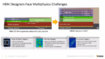
For many years, analog IP was typically developed in older nodes. There have been many advances over the past few years that have changed this paradigm. Today, sensing and communication must be integrated on-chip with cutting edge technology. Analog Bits has met this challenge with a broad range of IP to address the needs of the latest AI and data center chip designs.
What was the biggest challenge your company faced in 2024?
The best way to describe this is a multi-dimensional balancing act. We need to deliver high-speed, high-precision IP that runs at the most advanced nodes with the lowest possible power. Achieving that combination requires a lot of analyses and tradeoffs.
How is your company’s work addressing this biggest challenge?
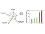
There are technical achievements that are certainly needed. For example, thermal considerations are top of mind for many design teams. To help with that we’ve developed a comprehensive on-die sensing IP portfolio. This technology helps to manage power, enhance reliability, and improve yield. Timing glitches are also becoming more prevalent in advanced designs. We also have a portfolio of glitch detection IP to address this growing problem. There are many more areas we cover, you get the idea.
But there is also an industry-level shift in thinking that is coming. For a long time, analog IP choices were made at the end of the design process. It was something of an afterthought to finish the design. I liken this to package design. For many years, the package for a monolithic chip was done near the end of the design to finish things up. With the growth of multi-die design, the package team is now an integral part of the system development team – the choices made impact and enable the entire project.
In the new multi-die environment, enabling IP that unlocks optimal power distribution, high-speed communication and eases thermal stress becomes a cornerstone item for system design. This is the IP that Analog Bits provides, and I am making changes to the company’s structure to allow us to be part of the system architecture team, ensuring all demands can be met early in the architectural definition phase. You will be hearing more details of how Analog Bits is moving upstream to address substantial challenges as early as possible.
What do you think the biggest growth area for 2025 will be, and why?
Thanks to the huge increase in data center expansion and AI application development, energy efficiency with superior performance and latency are an absolute requirement. To achieve these requirements, superior clocking, sensing, I/O and SerDes communication are all needed. This will be a big growth area, and these are all sweet spots for Analog Bits.
How is your company’s work addressing this growth?
Beyond design excellence, we focus on partnering with foundries and leading suppliers. A good example of this is the work we’ve done with Arm.
We worked on several integrated power management and clocking IPs with the company. Arm’s customers can readily use these solutions in N3P and soon in N2P. LDO regulator IPs were also part of the effort to efficiently manage the large absolute and dynamic current supplies to Arm CPU cores.
A case study of how CPU cores seamlessly integrate with Analog Bits LDO and Power Glitch Detector IPs, along with integrated clocking capabilities was presented at TSMC OIP in 2024. The implication of this work is substantial for advanced data center applications.
And our focus on working with system design teams early will clearly have a positive impact as well.
What conferences did you attend in 2024 and how was the traffic?
Beyond the usual industry trade shows such as DAC, Analog Bits supports many of the events of our foundry partners. We attend all the worldwide events for the TSMC Technology Symposium, TSMC OIP Ecosystem Forum, Samsung SAFE Forum, GlobalFoundries Technology Summit and Intel Foundry Services Direct Connect events. Each event brings us closer to key customers and our foundry partners, so we view them as all quite valuable.
Will you attend conferences in 2025? Same or more?
Each event we attended last year allowed us to reach an important segment of our customer base and partner network. I expect we will have a similar program this coming year. You can view the current plans on our website at https://www.analogbits.com/events/.
How do customers engage with your company?
As discussed, we are at a lot of shows. You can come by our booth, get the latest information and start a conversation with us. We also joined the Silicon Catalyst In-Kind Partner Ecosystem last year, so if you’re a startup in that incubator it’s easier to work with us. We also opened a new design center in Prague last year. You can also get things started by dropping a note to info@analogbits.com.
Additional questions or final comments?
2024 was a great year for Analog Bits and we’re excited to see the expansion on the horizon in 2025. If you’re working on advanced data center or AI applications, things just got a bit easier. If power management, performance or communication are challenges we can help.
Also Read:
Analog Bits Builds a Road to the Future at TSMC OIP