You are currently viewing SemiWiki as a guest which gives you limited access to the site. To view blog comments and experience other SemiWiki features you must be a registered member. Registration is fast, simple, and absolutely free so please, join our community today!
It is well-known that AI is upending conventional wisdom for system design. Workload-specific processor configurations are growing at an exponential rate. Along with this is an exponential growth in data bandwidth needs, creating an urgency for 1.6T Ethernet. A recent SemiWiki webinar dove into these issues. Synopsys and Samtec explored many of the challenges to face on the road to extreme data bandwidth.
An example is the critical role of 224G SerDes in enabling high-speed data transfers and the importance of rigorous interoperability testing across all parts of the channel. Other topics are covered, including a look at what comes after 1.6 Terabits per second (Tbps). A replay link is coming but first let’s look at what’s discussed in the webinar – Achieving Seamless 1.6 Tbps Interoperability with Samtec and Synopsys.
The Speakers
The quality of most webinars is heavily influenced by the expertise of the speakers. For this webinar, there are two knowledgeable, articulate presenters that provide a great deal of valuable information.
Madhumita Sanyal
Madhumita Sanyal is the director of technical product management for the high-speed Ethernet, PCIe, and D2D IP portfolio at Synopsys. She has over 20 years of experience in ASIC design and the application of logic libraries, embedded memories, mixed-signal IPs, and design methodology for SoCs in high-performance computing, automotive, and mobile markets.
Matthew Burns
Matt Burns develops go-to-market strategies for Samtec’s Silicon-to-Silicon solutions. Over the course of 25 years, he has been a leader in design, applications engineering, technical sales and marketing in the telecommunications, medical and electronic components industries. He currently serves as Secretary at PICMG.
Topics Covered
The webinar focused on the requirements for SoC design to achieve interoperability for the high bandwidth, high-performance computing required for AI/ML workloads. Madhumita and Matt cover a lot of topics, but they get through all of it in about 40 minutes. Very efficient. This is followed by approximately 15 minutes of live questions from the webinar audience. The topics covered are:
Introduction
Triggering new protocols like UAL for scale-up, and UEC for scale-out with an underlying line-rate of 224
Why ecosystem enablement is important
What capabilities in 224G SerDes can help achieve industry requirements for scale-up and scale-out
Interconnect needed to build 224G data center system topologies
Interop setup and demo
448G channel look-ahead
Synopsys summary
Samtec summary
Q&A
Before I get into some more details, a definition of scale-up and scale-out would be useful.
Scale-up, also known as vertical scaling involves adding more resources to existing infrastructure to handle increased workloads. Scale-out, also known as horizontal scaling involves distributing workloads across multiple resources.
What follows are some highlights of the topics covered in the webinar.
Madhumita began with an overview of the substantial bandwidth demands of new AI architectures. She referred to the bandwidth gap, as shown in the figure on the right. This increase cannot be addressed by doing more of what was done before. New architectures supported by new protocols are required as systems are both scaled-up and scaled-out.
She then provides a lot of details on how approaches such as Ultra-Ethernet and UALink_200 can help to address the challenges ahead. Madhumita provides details regarding various architectures that can achieve both scale-up and scale-out requirements. She discusses the various characteristics of passive copper cable, active copper cable and optical modules and where each fit.
Both short and long reach capabilities for 224G channels are explored in detail with specific requirements for SerDes technology. Architectural details and waveforms are shared. She also covers the specific requirements of the simulation environment and the requirements of the models to drive the process. Madhumita concludes with an overview of the interoperability requirements of the Synopsys SerDes and the pallet of solutions offered by Samtec to complete the implementation. She shares a list of technologies that are used for interoperability validation that includes:
224G loopback with Samtec Si-Fly® HD Near Chip Cable Assembly 64 port, 40dB+ channels
24G loopback with 1m DAC + MCBs
224G electrical loopback with Samtec Si-Fly® HD Near Chip Cable Assembly 32 port, 40dB+ channels
224G electrical loopback with Samtec Bulls Eye® ISI Evaluation Boards
Matt then discusses the changes Samtec is seeing in system topologies in the data center, including disaggregated memory. Scalable, flexible, high-performance interconnect becomes a critical requirement. This is where Samtec is focused. Matt began with the diagram below that summarizes the various Samtec interconnect products that facilitate 224 Gbps PAM4 operation from the front panel to the backplane.
He spends some time explaining the various components in this diagram, both optical and copper as well as the benefits of Samtec Flyover® technology. The benefits of Samtec’s Si-Fly® HD co-packaged copper interconnects are also discussed. Some of the features Matt discusses in detail include:
Ultra-high-density co-packaged substrate-to-cable
Highest density interconnect supporting 224 Gbps PAM4 (170 DP/in2)
Designed for high density interconnect (HDI) & package substrates
Matt then provides detailed performance data for various Samtec interconnect configurations along with the architectural benefits of each approach. Both short and long reach configurations are discussed. Matt describes some of the work Samtec is doing with its OEM and OSAT partners to prove out various configurations.
Matt then provides details of a recent live demonstration with Synopsys to illustrate the interoperability of Synopsys communication IP and Samtec channel solutions.
Joint Synopsys/Samtec Demo @ SC24
Matt concludes with a discussion of the work underway for 448 Gbps channels. While still in development, Matt shares some details of what to expect going forward. Both Matt and Madhumita then finish with an overview of the capabilities of each company to address high-speed channels, both now and in the future. This is followed by a spirited Q&A session with questions from the live audience.
It Takes a Village
I had the opportunity to chat with Matt Burns a bit after the webinar. I’ve known Matt for a long time and always enjoy hearing his perspectives on the industry since Samtec typically looks at system design challenges a bit differently than a chip company. Matt began our discussion with this statement:
“If I’m an OEM or an ODM and I’m trying to implement 1.6T ports, there’s no one solution provider I can go to for the whole thing. It takes a village.”
Matt went on to describe the types of IP, physical channels, simulation models and methodology required to get the job done. In this situation, interoperability is key and that’s why working with leading companies like Synopsys is so important to Samtec. This is how real-world solutions are proven and adopted in the market. Matt felt a lot of the details of this formidable task are covered in the webinar, so now it’s time to access the webinar replay.
To Learn More
If AI is part of your next design, you will face the need for high-performance channels and the Samtec/Synopsys webinar delivers a lot of the details you will need. You can access the webinar replay here. And that’s the webinar – Achieving Seamless 1.6 Tbps Interoperability with Samtec and Synopsys.
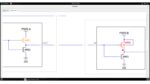
In the realm of mixed signal design for integrated circuits (ICs), level shifters play a critical role for interfacing circuits that operate at different voltage levels. A level shifter converts signal from one voltage level to another, ensuring compatibility between components. Figure 1 illustrates a missing level shifter between power domains.
Figure 1. Missing level shifter between two power domains is a common mistake that is being encountered in the analog-digital mixed signal design.
It’s not uncommon for a member of the design team to miss a level shifter while designing a largeIC. . Although a seemingly obvious mistake, there are a plethora of pragmatic factors that may contribute towards a mistake like this in a large complex design. Some are them are assumption of voltage levels, lack of documentation of specifications, time constraints, complexity of design, inexperienced designers, inadequate simulation and testing and using a previous design as reference.
Depending upon the design team and company size, and the time constraints and resources available for a particular project, one or more of these checkpoints may or may not be available. If absent, the likelihood of design mistakes to inadvertently slip through before fabrication significantly increases.
The difficulty of accurately identifying the need for a missing level shifter, despite all kinds of checkpoints, presents an opportunity for the electronic design automation (EDA) industry to provide a more robust solution that can avoid these all too common human mistakes.
Consequences of a missing level shifter
A missing level shifter in an IC design can have profound consequences that may completely compromise the integrity, performance and even power consumption of the design. Some examples of the consequences that may occurs due to missing level shifter somewhere in the design are:
Signal integrity issues
Damage to devices
Increased power consumption/leakage
Reduce performance
Compatibility issues
Noise sensitivity
Figure 2 shows a diagram of an IP with two power domains. When both power domains are powered-up and the voltage difference between the power domains is less than a threshold value (which you can set in the simulator), there are no issues in the design. However, if the voltage difference is greater than the threshold value, let us say Power domain 2 is operating at a higher-voltage level than Power domain 1, then a logic ‘1’ at Power domain 1 can be assumed a logic ‘0’ at Power domain 2. This leads to incorrect data transmission.
Figure 2: A block level diagram of an IP with multiple power domains.
An optimal solution for identifying inter-domain power leakage
The first step towards finding an inter-domain power leakage is finding all DC paths between all power domains. This step is immensely helpful and will list out all possible combinations of DC paths possible between two or more power domains. This step finds every single combination of paths that may exist between two or more power domains. Fortunately, this first step of finding all DC paths is relatively easy.
After finding all DC paths and identify crossings between different power domains, the tool performs a sophisticated evaluation to determine whether these crossings actually require level shifters. This complex analysis demands a comprehensive understanding of the circuit’s architecture and power domain interactions.
The determination of missing level shifters requires detailed voltage analysis that can only be accomplished through advanced EDA tools. These tools examine critical voltage relationships, specifically the gate-to-source voltage in PMOS devices and gate-to-drain voltage in NMOS devices. The measured voltages are compared against expected values, which are derived from the respective power and ground rail specifications for each domain. When these voltages deviate from expected values, it signals a potential requirement for level shifting.
Siemens EDA offers an innovative tool called Insight Analyzer that can quickly and accurately identify the risk of missing level shifters between power domains, as well as many other circuit reliability issues that are not easily identified using simulation or traditional electrical rule checking tools. Insight Analyzer uses a form of state-based analysis at the pre-layout stage without the need for simulation, so designers can perform early design analysis during the development process. This early, shift-left, analysis makes the design process more efficient, saving time and money.
Conclusion
As semiconductor technology reaches new heights and chip designs are becoming more complicated, with multiple power domains and multiple power states, the risk of missing a level shifter by the designer becomes all too real. The risk of not catching these design elements until much later in the design phase or even post fabrication is at all-time high, with there always being a complicated sets of instances and circumstances which may lead to designer missing a level shifter in the early design phase. The Insight Analyzer tool provides circuit designers with a designer- driven reliability verification flow, capable of running full-chip, transistor-level circuit analysis. Using Insight Analyzer enables circuit designers to improve their design reliability in today’s fast paced environment. You can learn more in my new technical paper Finding missing level shifters between power domains with Insight Analyzer.
About the author, Bhanu Pandey
Bhanu Pandey is a product engineer for Calibre Design Solutions at Siemens Digital Industries Software, with responsibility for the Insight Analyzer circuit reliability analysis tool. His focus and technical experience are in analog circuits. Prior to joining Siemens, Bhanu worked as an analog design engineer. He received his Master of Science degree in Electrical and computer Engineering from Georgia Institute of Technology.
I last wrote about Secure IC back in 2023, a provider of embedded security technologies and services. Cadence announced at the beginning of 2025 their intention to acquire this company, which warrants a check-in again on what they have to offer. Secure-IC addresses multiple markets, from automotive, through defense/space and more. The central value is security management all the way through a product lifecycle, from initial design through manufacturing, provisioning, mission mode and ultimate decommissioning.
First, where are markets at on security?
We all understand that security is important, but just how important? According to Karthik Raj Shekar (FAE lead and Project Manager at Secure-IC), active engagement is accelerating. Where once security features were a checkmark, now they are must-have in automobile, mobile, server applications, defense (of course), smart cards and payment apps.
That demand is evolving is not surprising. Take automotive where new capabilities create new potential attack surfaces, through telematics or V2X for example. Even more critically, over-the-air updates with an ability to change core software demand high levels of protection.
What I found interesting is that pressure to get serious about security is being driven top-down. OEMs are being held to must-comply security standards, either regulatory or though guidelines/ad-hoc requirements. They push these down their supply chains not as checkmarks but as specific compliance expectations. Now Karthik sees chip makers becoming very proactive, anticipating where they will need to be versus coming security demands across a broad swath of markets. Which leaves me wondering which products can still ignore security. $60 porch-pirate cameras perhaps, but not security cameras providing guarantees. Cheap drones, but not high-end drones. Opportunities for non-compliant chips will still exist, but likely not in the big $$ markets.
Secure-IC solutions
The company provides a comprehensive palette of solutions, from embedded hardware and software which can be built into your chip design, to server solutions running in the cloud for fleet management, to security evaluation tools from design through post-silicon, to side-channel and fault injection vulnerabilities as a service provided by Secure-IC experts.
The design solution starts with a root of trust they call Securyzr, providing a very broad set of security services. These include of course attestation, key management, crypto options (including post-quantum options), secure connectivity, secure boot and trojan detection. Also some wrinkles I haven’t heard of elsewhere: ability to do post-silicon trimming for sensors (which can be controlled from the cloud-based server), and an AI agent embedded in the device software to reduce false alarms and ensure only important information is sent to the cloud server.
The cloud server is an integral part of the complete solution, allowing you to manage the security of a fleet of products. Here you can control provisioning (assigning keys to newly commissioned products, secure firmware update over the air and extensive monitoring options. As noted above, you can monitor and tune sensors, even turn malfunctioning sensors off to adapt to change conditions in the field and among the fleet. Here integrated device security and cloud-based management makes sense. I’m not sure how a standalone cloud security platform could manage down to sensor-level tuning. Maybe at some point. One more important point – they also provide support for Product Security Incident Report Teams (PSIRT). Security is a dynamic domain as we all see in regular OS and product update requests. PSIRT support helps OEMs stay on top of latest zero and one-day threats for their own products. Ultimately when you want to take a product out of service, the cloud service will support decommissioning, ensuring that expired credentials cannot be hijacked by a threat actor to pose as a legitimate member of the fleet.
If you are selling into security-sensitive fields ultimately you will need to prove compliance through an authorized neutral lab. Getting ready for such testing can consume significant expert time and effort. Security-IC tracks relevant standards very closely: PSA, Autosar MCAL, TPM2.0, PKCS#11, Common Criteria, FIPS, etc, and can provide expert assistance and tools to do gap analysis on your design against the appropriate requirements for your target markets. They will also (optionally) help with side-channel and fault insertion analysis, both areas demanding high expertise to track down weaknesses.
Altogether this looks like a very comprehensive suite of solutions. You can learn more about Secure-IC HERE.
Prolog – Interface Protocols: Achilles’ Heels in Today’s State-of-the-art SOCs
June 30 was only a week away when Varun had a sleepless night. The call from the datacenter manager the evening before alerted him on a potential problem with the training of a new Generative AI model. Six months earlier Varun’s employer installed the latest generation of a leading-edge ML accelerator that promised to cut the training time of the largest GenAI models by 50% via stellar processing bandwidth and reduced latency. Previously, training the largest LLMs, boasting over a trillion parameters, on the then state-of-the-art accelerators took approximately one year to achieve a satisfactory level of confidence. This process involved leveraging high-quality training data to minimize hallucinations. On paper all was perfect if not for a little secret unknown to most: the loss of even a single data packet during training could necessitate retraining the entire AI model. The secret became a mantra in the Gen AI community: “Start and Pray.”
The grim scenario described above is just one of many with potentially catastrophic consequences unfolding across various cutting-edge industries today. From autonomous vehicles making split-second life-or-death decisions to AI-driven medical systems managing critical diagnoses, the stakes have never been higher. Yet, these industries share a disturbingly common vulnerability: malfunctions in interface protocols.
Part 1 of 2. The Evolution of Interface Protocols: From Supporting Components to Critical Elements in Modern SoC Designs
Part 1 presents a comprehensive overview of the evolution of Interface Protocols, tracing their journey from auxiliary support components to indispensable pillars in cutting-edge HPC SoC designs. These protocols now underpin not only everyday technologies but also mission-critical, complex AI applications. The section explores the key drivers behind the rapid advancement and frequent upgrades of existing protocols, as well as the innovation fueling the development of entirely new standards.
Brief Historical Perspective of Interface Protocols
Interface protocols have their origins in the early development of computer systems, dating back to the 1950s and 1960s, when computers transitioned from isolated, monolithic machines to interconnected systems. For most of the time since their inception, the design of Interface Protocols has been driven primarily by the need for connectivity between different components of a computer system or between different systems themselves. As the electronic industry expanded, Interface Protocols facilitated the interoperability of components sourced from different vendors.
Over the past decade, the landscape of Interface Protocols has undergone a profound transformation. Technological advancements have created new demands for higher performance, shorter latency, greater power efficiency, improved reliability, and enhanced security, all of which have driven significant changes in interface protocol design and development. These evolving requirements are now central to a wide range of applications, from consumer electronics to industrial systems, automotive, and more.
As a result, modern System-on-Chip (SoC) development priorities have shifted dramatically. Performance is no longer the sole focus; energy efficiency, data integrity, and robust security are equally critical.
See Sidebar: Seven Decades of Interface Protocols Development.
Key Drivers Shaping the Evolution of Modern Interface Protocols
The evolution of modern interface protocols is shaped by two major, yet opposing, industry trends. On one hand, the rapid growth of software development has shifted System-on-Chip (SoC) functionality from hardware-centric implementations to software-defined solutions. On the other hand, the meteoric rise of artificial intelligence (AI)—especially predictive and generative AI—has reintroduced heavy compute and data manipulation demands, moving the focus back to SoC hardware.
Software’s Dominance: Transforming SoC Development
In his influential 2011 article, “Why Software Is Eating the World,” Marc Andreessen predicted the transformative power of software across industries. Over the past decade, this vision has materialized, driving profound changes in SoC design.
The shift to software-defined solutions has revolutionized the development process by offering greater flexibility, faster time-to-market, and simplified post-release updates. Developers can now enhance and scale SoC functionality without requiring costly hardware redesigns. These advantages have significantly streamlined the SoC lifecycle, enabling rapid responses to changing market demands.
However, this transition has brought its own set of challenges:
Data-Intensive Operations: Software’s growing reliance on large datasets demands substantial memory capacity.
Energy Consumption: The continuous transfer of data between memory, processing elements, and interfaces consumes significant power.
AI’s Impact: Redefining SoC Hardware Requirements
The rise of AI has compounded these challenges while introducing a third. Predictive and generative AI applications require processing engines capable of handling massive data loads with minimal latency.
Traditional CPUs often fall short, as their architecture struggles with the bottlenecks of data movement between memory and compute units. To address these demands, the industry has embraced GPUs, FPGAs, and specialized AI accelerators, which excel at handling high-throughput workloads.
Yet even the most advanced processors face limitations if data delivery speeds cannot keep up. When memory and I/O protocols lag, high-performance processing units risk underutilization, idling while waiting for data. This highlights the critical importance of modernizing interface protocols to meet AI’s escalating data demands and fully leverage advanced SoC capabilities.
Implications on Interface Protocols by Key Industry Trends
As AI and software continue to drive innovation, balancing these opposing trends will require advances in memory and I/O protocols, leading to the rapid evolution of existing protocols and the emergence of new protocols.
Implication on Complexity
As modern SoCs designs have grown in complexity, the embedded Interface Protocols that interconnect them have also progressed at an extraordinary pace.
High-performance protocols, such as the latest iterations of PCIe—from Gen 4 to the cutting-edge Gen 7—have evolved into highly complex systems. The PCIe Gen 7 specifications alone now encompass over 2,000 pages, underscoring the complexity needed to enable advanced functionality. Furthermore, implementation complexity continues to escalate as data transmission speeds push the physical limits of what is achievable, challenging both design and manufacturing processes.
Implication on Performance
Cloud infrastructures, AI algorithms, and generative AI applications are fueling an unprecedented demand for data, both in volume and in processing power. This surge drives the need for massive memory capacities, higher communication bandwidth, lower latency, and significantly enhanced throughput.
Traditionally, achieving faster data transfer rates in new protocol generations was accomplished by physically positioning on-chip components closer together. However, modern protocols must now support connections over longer distances, where both bandwidth and latency become critical challenges.
Evolution of Existing Interface Protocols and Emergence of New Interface Protocols
In the fast-changing landscapes of AI, machine learning, and big data analytics, established protocols such as PCIe, Ethernet, and memory interfaces have undergone significant evolution to meet the growing demands for larger capacity and higher performance. As AI software workloads generate vast amounts of data, traditional data transfer mechanisms have faced challenges in keeping pace, resulting in inefficiencies affecting processing power, latencies and power consumption. Research highlights that moving data via DRAM consumes up to three orders of magnitude more energy than performing arithmetic operations on the data, making memory-related power consumption a critical bottleneck in high-performance computing environments.
The surge in demand for memory bandwidth and capacity has begun to exceed the capabilities of existing protocols. Consequently, well-established technologies like PCIe have had to evolve continuously, leading to innovations such as PCIe 7.0 and beyond. Meanwhile, new solutions like Compute Express Link (CXL) have emerged to address these limitations, offering greater flexibility in how memory and accelerators are connected. CXL enables cache coherency and shared memory resources across CPUs, GPUs, and other accelerators, enhancing efficiency and cost for workloads like AI inference and data analytics.
Simultaneously, multi-die architectures, which integrate multiple dies or chiplets within a single package, have introduced transformative improvements in data movement between processing units. By bringing these dies physically closer together, communication between them becomes faster and more power-efficient, significantly reducing latency.
Evolution of Existing Protocols
Existing protocols have been evolving at an increasingly rapid pace. One prominent example is PCIe, which has now advanced to PCIe Gen 7, set for release in 2025. Even as Gen 7 approaches, the PCI-SIG (Peripheral Component Interconnect Special Interest Group) is already discussing the specifications for PCIe Gen 8, highlighting the urgency of keeping up with growing performance needs. See Table I
TABLE I: Bandwidth and latency specification of seven generations of PCIe. (*) PCIe 7.0 not released yet, specifications are estimated.
The evolution of Ethernet has been even more dramatic. Ethernet standards, particularly those supporting speeds up to 10 Gbps, have undergone more than a dozen amendments in the past five years alone, with the rate of updates accelerating. Ultra-Ethernet, currently under development by the Ultra Ethernet Consortium (UEC), which includes leading companies in AI and networking like AMD, Intel, and HPE, is specified to support transfer speeds of up to 224 GB/sec. For context, this is nearly twice the speed anticipated from PCIe Gen 7 and positions Ultra-Ethernet as a direct competitor to Nvidia’s NVLink[i], which offers a bandwidth of 480 GB/sec.
TABLE II: Bandwidth and latency specification of five generations of Ethernet. (**) Ethernet 800GbE not released yet, specifications are estimated
Memory protocols are advancing at a similarly rapid pace. DDR (Double-Data-Rate) memory has reached its sixth generation, while HBM (High-Bandwidth Memory) is now in its third generation, offering a bandwidth of up to 800 GB/sec. These developments in memory protocols are crucial for supporting the growing data needs of AI and high-performance computing (HPC) environments.
Emergence of New Protocols
In parallel with the evolution of existing protocols, entirely new protocols are being designed to address the unique demands of AI accelerator engines, where high bandwidth and low latency are critical. Some of the most groundbreaking new protocols include UCIe (Universal Chiplet Interconnect Express), UAL (Ultra Accelerator Link), and UEC (Ultra Ethernet Consortium). These protocols are specifically engineered to ensure interoperability across diverse ecosystems while maximizing performance, increasing data bandwidth, and improving power efficiency. They also are designed with a emphasis on security to ensure reliability and security of data transfer critical in AI and cloud-based systems.
In summary, the rapid evolution of existing protocols, coupled with the emergence of new ones, is driving the technological infrastructure required to support the next generation of AI and data-intensive applications like autonomous driving vehicles.
Conclusions
The increasing complexity of SoC software, along with the rapid evolution of SoC hardware and rising performance demands, is pushing the design community to continuously innovate and extend the boundaries of interface protocols, all while ensuring efficiency and reliability. Modern interface protocols are designed with flexibility in mind, allowing them to adapt to diverse applications and workloads. This ongoing evolution fosters deeper integration between hardware and software, enabling SoC designs to deliver highly optimized solutions that balance performance, efficiency, and security.
Verifying the functionality and performance of these advanced protocols in sophisticated, software-driven systems demands a blend of high-performance hardware-assisted verification and protocol verification technologies built on proven protocol IP implementations. The rapid pace of protocol innovation necessitates aggressive roadmaps that match IP advancements with verification technologies, ensuring alignment with the tight time-to-market schedules critical for HPC market leaders.
As these protocols evolve, they will play a critical role in shaping the next generation of interconnected systems, expanding the possibilities in fields like artificial intelligence, autonomous systems, and cloud computing.
—
Sidebar – Seven Decades of Interface Protocols Evolution
The origins of Interface Protocols date back to the early days of computing in the 1950s and 1960s, when they were initially developed to enable communication between different components within a computer. These early protocols were often proprietary and hardware specific. However, over time, they evolved into standardized systems designed to facilitate seamless connectivity, communication, compatibility, interoperability, scalability, and security across devices and systems from multiple vendors.
As technology advanced, Interface Protocols became more sophisticated, secure, and universal, playing a crucial role in ensuring the smooth operation of increasingly complex computing environments. Over the course of seven decades, these protocols have been integral to the evolution of communication technologies.
1950s: Early Computer Systems and Proprietary Protocols
In the early days, computers like the UNIVAC and IBM 700 series used proprietary protocols to communicate with peripherals like punch card readers, printers, and tape drives.
1960s: Rise of Serial Communication and Early Networking
With the proliferation of peripherals and modems, the need for a protocol to transfer data over simple connections led to the development of the RS-232 standard, one of the most widely used serial communication protocols.
1970s: Networking and Early Standardization
In 1973, Xerox PARC developed the Ethernet protocol for local area networks (LANs) that quickly became the dominant standard for connecting computers within an area, enabling faster and more reliable communication.
Around the same time, ARPANET conceived the TCP/IP suite to provide a scalable protocol for interconnecting different networks. It set the stage for the Internet.
1980s: Expansion and Global Standardization
In the 1980s, the Small Computer System Interface (SCSI) standard was developed to connect peripherals as hard drives, scanners, and others to host computers.
1990s: Internet and Security Computing Peripherals Protocols
With the rise of the World Wide Web, HTTP (Hypertext Transfer Protocol) and HTML (Hypertext Markup Language) became fundamental to web communication. HTTP facilitated the transfer of web pages between clients (browsers) and servers.
The Universal Serial Bus (USB) standard, introduced in 1996, supported data transfer rates of 1.5 Mbps (Low-Speed) and 12 Mbps (Full-Speed), significantly improved over serial and parallel ports. It became a crucial protocol for connecting devices such as keyboards, mice, and storage drives to computers, offering plug-and-play functionality.
2000s: Wireless Communication and Computing Peripherals Protocols
Wi-Fi: Wireless communication protocols, particularly Wi-Fi (based on the IEEE 802.11 standard), became increasingly important in the 2000s as mobile computing and smartphones gained popularity.
Bluetooth: Bluetooth emerged as a short-range wireless protocol for connecting personal devices such as headphones, speakers, and wearables.
The USB has seen more than 10 upgrades since its inception. The latest USB4 v2.0 released in 2022 supports a max bandwidth of 80 Gbps.
2010s-Present: High Performance and Secure Data Transfer
PCIe, Ethernet and Memory protocols underwent several upgrades in rapid progression and emerged as the de-facto standards for AI and datacenters.
[1] The NVLink Switch is the first rack-level switch chip capable of supporting up to 576 fully connected GPUs in a non-blocking compute fabric. The NVLink Switch interconnects every GPU pair at an incredible 1,800GB/s.
As RISC-V adoption accelerates across the semiconductor industry, so do the concerns about hardware security vulnerabilities that arise from its open and highly customizable nature. From hardware to firmware and operating systems, every layer of a system-on-chip (SoC) design must be scrutinized for security risks. Unlike software, hardware is extremely difficult to patch after deployment—making early vulnerability detection critical. The rapidly growing number of hardware CVEs (Common Vulnerabilities and Exposures) reported by NIST underscores the seriousness and increasing sophistication of hardware-based threats.
At the core of these vulnerabilities are underlying weaknesses—the root causes that leave a system exposed. A weakness, as defined by MITRE, is a design flaw or condition that could potentially be exploited. These are cataloged in the Common Weakness Enumeration (CWE) database, while actual vulnerabilities (exploitable instances of those weaknesses) are tracked in the CVE database.
At Andes RISC-V CON last week, Will Cummings, senior security applications engineer from Cycuity, gave a talk on enhancing RISC-V CPU security.
MITRE CWE Framework for Hardware
MITRE’s CWE is a well-established, open framework in software and a growing presence in hardware. It now includes 108 hardware-specific CWEs across 13 categories, providing a structured and actionable way to identify, prevent, and verify fixes for known hardware design weaknesses. Categories include areas such as general logic design, memory/storage, cryptography, and transient execution, among others.
Why CWEs Matter for RISC-V
RISC-V and CWE share a foundational philosophy of security through openness. RISC-V, developed collaboratively as an open standard, aligns with Auguste Kerckhoffs’ principle: a system should remain secure even if everything about it is public. Similarly, CWE is an open, community-maintained repository that promotes transparency and standardization in security classification. This shared ethos makes CWE a natural fit for securing RISC-V designs.
Security analysis of typical RISC-V processor IPs shows that roughly 65% of all 108 hardware CWEs are applicable. In some categories—like core logic, memory, cryptography, and debug/test—over 70% of CWEs are relevant. This makes CWE a powerful tool for prioritizing and addressing security concerns in RISC-V development.
New Microarchitectural CWEs for Transient Execution
In early 2024, MITRE introduced new CWEs targeting microarchitectural weaknesses, developed with contributions from Arm, AMD, Cycuity, Intel, and Riscure. These CWEs address vulnerabilities associated with transient execution attacks, which have gained prominence because of exploits like Spectre and Meltdown:
CWE-1421: Shared Microarchitectural State — Core to most transient execution attacks
CWE-1422: Stale Data Forwarding — Enables forwarding of data to a shared resource
CWE-1423: Integrity of Predictors — Focuses on corrupted branch predictors
These weaknesses fall under CWE-1420: Exposure of Sensitive Information during Transient Execution, which is itself part of the broader hardware design category under CWE-1194.
A Structured Approach to Security: From Weakness to Verification
The proposed CWE-based framework maps weaknesses to specific security protection requirements, which then support yet more specific security properties. These in turn yield evidence from simulation, emulation, or formal methods. This structure helps ensure that every security requirement is grounded in a recognized weakness and backed by verifiable proof.
Cycuity plays a vital role in this process by offering early-stage security verification for hardware design. Its flagship product, Radix, uses information flow analysis to track how secure assets (e.g., encryption keys) move through hardware, firmware, and across boundaries between secure and non-secure domains. It simulates how attackers might exploit design flaws such as improper access control or leakage via shared microarchitectural resources, enabling early detection—before the chip is even built.
While Radix is well-aligned with RISC-V’s modular architecture, it is architecture-agnostic and effective across all processor architectures and custom silicon as well. It integrates easily into standard SoC development workflows, including simulation, emulation, and formal verification environments. It also supports firmware-in-the-loop analysis and aligns with industry standards like CWE—ensuring security is both proactive and measurable.
Mutual Benefit: MITRE and RISC-V
MITRE and RISC-V International benefit from each other through their shared commitment to openness, transparency, and community collaboration. RISC-V offers a flexible, open platform where MITRE’s security frameworks like CWE can be directly applied and validated. In turn, MITRE enhances RISC-V security by enabling a systematic, standard-based approach to identifying and mitigating hardware design flaws.
Summary
The CWE framework provides a practical, structured methodology to enhance RISC-V security—starting from known weaknesses, mapping them to protection goals, and verifying that those goals are met. Combined with tools like Radix from Cycuity, which enable scalable, architecture-agnostic vulnerability detection, the industry now has the means to address hardware security earlier and more effectively.
As semiconductor technology scales and device complexity increases, accurately modeling the parasitic effects of metal fill has become critical for circuit performance, power integrity, and reliability. Metal fill is a crucial part of the manufacturing process, ensuring uniform layer density, improving planarization, and managing thermal and stress effects. However, the added metal fill structures also introduce parasitic capacitances that can significantly impact the behavior of the circuit.
What is metal fill and why is it important?
Metal fill refers to the addition of non-functional conductive structures in the layout to ensure uniform density across the chip. This is important for the planarization process during chemical mechanical polishing (CMP), as well as for thermal management and stress management during manufacturing. Without metal fill, there would be large open areas on the chip with little to no metal, leading to uneven deposition and thickness variations that are difficult to planarize. Figure 1 presents an example of a design with many metal fill shapes populating the empty areas in between signal nets.
Figure 1. An illustration of an IC design with dense metal fill structures in-between signal nets.
By adding these metal fill shapes, the density of each metal layer is evened out, enabling more effective CMP and better control over the final wafer topography. This improves the manufacturability and reliability of the chip. Metal fill also helps with thermal management by providing more conductive paths for heat dissipation, and it can help mitigate mechanical stress effects during processing.
However, the added metal fill structures also introduce parasitic capacitances that can significantly impact the behavior of the circuit. These parasitic effects can influence the chip’s timing, power integrity and overall performance. As a result, accurately modeling the impact of metal fill has become crucial for modern IC designs.
Limitations of traditional approaches
Traditionally, there has been a significant computational challenge in balancing the accuracy of parasitic extraction with the runtime required. Ignoring metal fill entirely oversimplifies the model, while extracting all parasitic components from the fill shapes is computationally expensive. This has led to two main approaches:
Ignoring metal fill until signoff
The simpler method is to ignore metal fill until the final signoff stage. The design is placed and routed, RC values are extracted, and static timing analysis (STA) is performed without considering metal fill. When the design is believed to be ready, metal fill is inserted, and RC extraction is rerun to account for the capacitive coupling. However, this late-stage addition of metal fill often results in timing violations that require numerous design modifications to resolve, delaying the project schedule.
Inserting metal fill during layout
The second approach is to perform metal fill insertion after each place and route step, enabling extraction and STA to account for the effects on every iteration. However, this adds significant time to the layout loop, as inserting metal fill on every layer can add hours to each iteration, slowing down the development process. The metal fill would still need to be verified during signoff, but there should be fewer violations that require design modifications.
These two approaches hint at an underlying tradeoff: modeling accuracy vs. computational efficiency. The most detailed modeling includes all metal fill as part of the parasitic extraction procedure with high accuracy, but at the cost of very high computational resources and processing time. Approximations will reduce the computational load, but at a cost to accuracy, leading to potential design errors not caught during simulation phases.
There are several ways to control the tradeoffs between accuracy and computational cost. For example, nets can be modeled as grounded or left floating, a decision with significant impacts on the accuracy of parasitic values calculated. Consider the options:
Floating, no reduction: Keep all fill shapes as floating in simulations and extract all of them for a more precise modeling of the actual physical design.
Reduction: Reduces the parasitic network of the fill shapes by analyzing the whole design to understand the impact of each fill shape. This generates a reduced netlist and maintains parasitic network equivalence to enable faster simulations.
Grounding: Assume floating nets are grounded to simplify the extraction process and reduce computational overhead.
Ignoring: Ignore all metal fill shapes and extract only signal nets. This is usually only used for debugging purposes.
The need for a new solution
These traditional flows are no longer sufficient for today’s large and complex chips. Designers need a solution that does not delay the schedule but still delivers high correlation to real metal fill in terms of extraction and timing accuracy
The solution is a smart and adaptive metal fill extraction technique that selectively focuses on the most impactful parasitic capacitances. This approach is an enhancement to the “reduction” method and can provide over 4x runtime improvements compared to conventional methods, while maintaining minimal impact on accuracy (figure 2).
An adaptive metal fill extraction technique dynamically adjusts the level of detail based on the design context, such as the density of signal nets versus fill shapes. This context-aware solution improves designer efficiency as semiconductor technology continues to scale and design complexity increases.
Figure 2: Chart comparing runtime for the different extraction techniques.
Conclusion: Enhancing productivity and reliability
Smarter metal fill extraction ensures that there are no unpleasant surprises late in the schedule, as the design team can be confident in the fast, accurate solution provided by the adaptive metal fill extraction technique. As semiconductor technology continues to advance, this type of smart, context-aware approach will become increasingly important for managing the complexity of metal fill and its impact on design implementation. This helps ensure the final IC product meets stringent performance and reliability requirements, even as semiconductor technology continues to scale.
About the author, Shehab Ashraf
Shehab is a product engineer for Calibre Design Solutions at Siemens Digital Industries Software, specializing in parasitic extraction. He received his BE in Electrical and Electronics Engineering from The German University in Cairo.
Recently, Design & Reuse held its IP-SoC Days event at the Hyatt Regency in Santa Clara. Advanced IP drives a lot of the innovation we are seeing in chip design. This event provides a venue for IP providers to highlight the latest products and services and share a vision of the future. IP consumers are anxious to hear about all the new technology conveniently in one place. Some of the presentations rose above the noise and made a substantial impact. This is a story of one of those presentations. Read on to see how Arteris is revolutionizing SoC design with Smart NoC IP.
Who’s Talking?
The presentation was delivered by Rick Bye, director of product management at Arteris. He also developed the content with Guillaume Boillet, senior director of strategic marketing at Arteris. These folks bring a lot to the table when it comes to advanced chip design.
Guillaume Boillet
Besides Arteris, Guillaume Boillet has worked at Synopsys, Mentor, Atrenta, ST-Ericsson, STMicroelectronics, and Thales. He has substantial experience in hardware design and EDA tool development and marketing with a focus on power optimization and connectivity. The skills he brings to Arteris are well-suited to the company’s broad footprint.
Rick Bye
Before joining Arteris, Rick Bye had a long career in the development of chips and IP for advanced communications and power management at companies such as Texas instruments, Broadcom, Zarlink Semi, Silicon Labs, NXP, and Arm. The combined knowledge and experience of these two gentlemen is formidable. The content developed and delivered at IP-SoC Days reflected that experience. A link is coming for the presentation but first let’s look at the topics covered.
What Was Discussed
Rick began with an overview of who Arteris is and where the company touches the semiconductor ecosystem. His first slide is an eye-popping overview of technical accomplishments and ecosystem impact. Once you click on the link below, you’ll get to see the incredible array of logos touched by Arteris.
In terms of corporate resume, there are also a lot of impressive statistics to review. Most folks know that Arteris is a system IP company. Some facts you may not know is that the company can claim 3.7B+ SoCs shipped in electronic systems, with 200+ active customers, and 850+ SoC design starts. The company’s products are used by 9 out of the top 10 semiconductor companies and the company has a 90%+ customer retention rate. There are plenty more accomplishments cited.
In terms of footprint, the focus is on overcoming complexity with maximum flexibility for optimized SoCs. There are three parts of this story, SoC Integration Automation, Network-on-Chip (NoC) Interconnect IP, and Network-on-Chip Interface IP. The balance of the presentation focused on the second item and how Arteris impacts design in this area. Regarding NoC usage, it was reported that there are typically 5-20 NoCs per chip or chiplet with NoCs representing 10-13% of the silicon.
The next section of the presentation examines semiconductor market dynamics. The emerging trends and the impact of AI are always interesting to hear about, and there are some great statistics presented. For those who have been in this industry for a while, you will be familiar with the projections made by Handel Jones at IBS. You will get to see Handel’s latest numbers, which are always interesting.
The next part of the presentation focuses on Arteris Smart NoC technology. There are two families of products here. Ncore delivers the requirements for cache-coherent interconnect IP, and FlexGen, FlexNoC, and FlexWay serve the needs for non-coherent Interconnect IP. The remainder of the presentation focuses primarily on the needs of the non-coherent portion of the design. The figure below illustrates where the non-coherent interconnect IP products fit.
FlexGen impacts a broad range of applications, so more details are presented on this technology. The graphic at the top of this post presents some of those details. To provide more context, here are some additional facts:
Challenge: SoC design complexity has surpassed manual human capabilities, requiring smart NoC automation. Modern SoCs have 5 to 20+ unique NoC instances and each instance can require 5-10 iterations.
FlexGen, smart NoC IP from Arteris delivers:
Productivity Boost: Accelerates chip design by up to 10x, shortening and reducing iterations from weeks to days for greater efficiency
Expert-Level Results: Enhances engineering efficiency by 3x while delivering expert-quality results with optimized routing and reduced congestion
Wire Length Reduction: AI-driven heuristics reduce wire length by up to 30%, improving chip or chiplet power efficiency
Connects any processor (Arm, RISC-V, x86) and supports industry protocols.
The presentation then dives into more detail about FlexGen and how it builds on FlexNoC technology for physical awareness. The core 80+ patent profile of Arteris in this area is explored and specific examples of performance and efficiency advantages are presented. The workflows involved are presented, along with specific examples of its impact.
To Learn More
I’ve just scratched the surface in this overview. You need to watch the complete presentation from IP-SoC Days to get the full picture of how Arteris can help with your next design. You can access a video of the complete presentation here. And that’s how Arteris is revolutionizing SoC design with Smart NoC IP.
Prior to becoming CEO of Pliops in 2023, Ido Bukspan was the senior vice president of the Chip Design Group at NVIDIA and one of the leaders at Mellanox before it was acquired by NVIDIA for nearly $7 billion.
Tell us about your company.
Pliops accelerates and amplifies the performance and scalability of global GenAI infrastructure, driving unparalleled efficiency and innovation.
Pliops was founded in 2017 by storage industry veterans from Samsung, M-Systems, and XtremIO. Pliops is pioneering a new category of product that enables cloud and enterprise data centers to access data up to 50 times faster with one-tenth of the computational load and power consumption. Its technology consolidates multiple inefficient layers into one ultra-fast device based on a groundbreaking approach. Pliops’ solution addresses the scalability challenges posed by the cloud data explosion and the increasing data demands of AI and ML applications.
What problems are you solving?
Pliops XDP LightningAI, our revolutionary Accelerated Key-Value distributed smart node, introduces a new tier of memory that surpasses HBM for GPU compute applications. Our product can double end-to-end performance and enhance efficiency for vLLM, a leading inferencing solution. By leveraging Pliops’ state-of-the-art technology, we deliver advanced GenAI and AI solutions, significantly improving GPU utilization, reducing total cost of ownership, and cutting power consumption and carbon emissions.
What application areas are your strongest?
Our strongest application areas focus on accelerating GenAI applications, including LLM inferencing, DLRM, RAG/VectorDB, and SQL and Document DB acceleration. Our users benefit from over 3X better utilization of compute resources, more than 50% savings in capital expenditures, and a 50% reduction in carbon footprint.
What keeps your customers up at night?
Our customers are deeply concerned about power consumption in data centers, especially as AI infrastructure and emerging AI applications significantly increase power footprints and strain cooling budgets. They also worry about maintaining margins as they expand their AI infrastructure, adding GPU tiers of compute. The growing power and cooling demands, combined with substantial capital expenditures on GPUs, are consuming margins and keeping our customers up at night.
What does the competitive landscape look like and how do you differentiate?
The competitive landscape in GenAI and applications requiring new infrastructure, including additional CapEx, cooling budgets, and increased power, is still emerging as we stand at the dawn of the AI revolution. Innovation is essential in this space, and we embrace all solutions, not just our own. Specifically, our focus is on enabling GPUs to have IO access to large amounts of data for local consumption by applications. There are various approaches to solving this, and our strategy is among them.
What new features/technology are you working on?
We are continually advancing our technology to meet the evolving demands of AI applications. Our latest developments include enhancements to our XDP LightningAI, which now provides unprecedented levels of memory and compute efficiency for GenAI workloads. We’re focusing on solutions that allow GPUs to access vast amounts of data for local processing, significantly improving performance and reducing energy consumption. Additionally, we are working on innovative methods to further decrease the power footprint and cooling requirements of data centers, ensuring our solutions remain at the forefront of sustainable AI infrastructure.
How do customers normally engage with your company?
We provide a comprehensive toolbox for critical GenAI applications, making it exceptionally easy for our customers to adopt our products and technology. Our solutions encompass silicon, hardware, and software components, and we offer reference designs that ISVs, CSPs, and operators can utilize with minimal effort to realize significant benefits. Our products are available as cloud-ready solutions, and we collaborate with compute/storage OEMs and ISVs to support HPC and on-prem data center operators.
Roger Cummings is the CEO of PEAK:AIO, a company at the forefront of enabling enterprise organizations to scale, govern, and secure their AI and HPC applications. Under Roger’s leadership, PEAK:AIO has increased its traction and market presence in delivering cutting-edge software-defined data solutions that transform commodity hardware into high-performance storage systems for AI and HPC workloads.
Roger is a seasoned entrepreneur and business leader with a distinguished track record of driving growth, innovation, and market leadership. Specializing in application infrastructure and AI/ML technologies, Roger has consistently identified emerging opportunities and built organizations that establish market dominance in rapidly evolving industries. Over his career, Roger has successfully guided five early-stage companies through highly successful acquisitions, raising over $1 billion in funding to fuel their global expansion.
In addition to his executive roles, Roger is an advisory board member at DevNetwork and an advisor at High Alpha Innovation. He has co-authored several papers on go-to-market strategies, operational excellence, and AI application infrastructure, reflecting his thought leadership in the field.
Tell us about your company?
PEAK:AIO is a pioneering AI infrastructure company specializing exclusively in data storage solutions engineered for Artificial Intelligence workloads. Unlike legacy IT storage vendors, our solutions are built from the ground up to match AI innovators’ exact needs and skill sets in the healthcare, government, life sciences, and advanced research sectors. Our mission is to eliminate bottlenecks in AI development by delivering unmatched speed, simplicity, and scalability.
What problems are you solving?
AI projects today often struggle with data bottlenecks caused by legacy storage solutions originally designed for traditional IT workloads. These outdated systems are typically complex, slow, energy-inefficient, and poorly aligned with the requirements of modern AI workloads. PEAK:AIO directly addresses these issues by providing storage infrastructure specifically designed for AI, eliminating data throughput limitations and significantly improving efficiency. We deliver up to six times the performance in one-sixth of the footprint, using just a fraction of the energy compared to traditional IT storage solutions.
What application areas are your strongest?
We excel in sectors where rapid access to vast datasets is crucial for successful AI outcomes, notably healthcare, life sciences, government, and large-scale AI research. Our technology underpins many significant AI initiatives, including pioneering deployments within the UK’s NHS and cutting-edge research collaborations with renowned institutions such as Los Alamos National Labs (LANL).
What keeps your customers up at night?
AI innovators, including data scientists, researchers, and medical professionals, worry most about their ability to rapidly and reliably access massive datasets needed to train complex AI models. They fear data bottlenecks that slow their projects, escalate costs and inefficiently use energy. Furthermore, managing complex, legacy storage infrastructure is not their core competency. Our customers need solutions that offer powerful simplicity, high performance, and extreme reliability, which is exactly what PEAK:AIO delivers.
What does the competitive landscape look like and how do you differentiate?
The competitive landscape is primarily populated by traditional IT storage vendors, which have adapted legacy solutions to attempt to meet AI needs. These repurposed offerings are usually complex, costly, and energy-intensive.
PEAK:AIO differentiates through purpose-built architecture optimized explicitly for AI workloads, delivering industry-leading performance, significantly lower energy use, and an unparalleled simplicity that fits the persona of today’s AI leaders, who are often highly skilled researchers and scientists who demand solutions that just work.
What new features/technology are you working on?
We are actively expanding our technology leadership by integrating advanced memory and storage architectures, such as CXL (Compute Express Link) and next-generation NVMe solutions, into our platforms. Additionally, we’re advancing our proprietary software-defined storage engine, designed to dynamically adapt storage tiers based on real-time AI workloads, continuously ensuring optimal performance and efficiency.
Additionally, we are evaluating vector database technologies and how this will help our clients.
How do customers normally engage with PEAK:AIO?
Customers typically engage through partnerships. We collaborate closely with each partner and customer to understand their specific AI infrastructure needs, and our specialist team provides personalized guidance, installation support, and ongoing optimization. This high-touch, expert-led engagement ensures our customers gain the maximum value and performance from their AI investments.
In this episode of the Semiconductor Insiders video series, Dan is once again joined by Anna Fontanelli, founder and CEO of MZ Technologies. In this discussion, more details of the challenges presented by advanced packaging and multi-die design are explored. Anna provides details of what’s involved in architectural exploration and interconnect management. She also provides some background on how MZ Technologies helps tame these challenges with its GENIO EVO platform.
The views, thoughts, and opinions expressed in these videos belong solely to the speaker, and not to the speaker’s employer, organization, committee or any other group or individual.