webinar banner AI 2026 v2

Voice as a Feature: A Silent Revolution in AI-Enabled SoCs

Voice as a Feature: A Silent Revolution in AI-Enabled SoCs
by Jonah McLeod on 05-26-2025 at 10:00 am

Voice as a Feature

When Apple introduced Siri in 2011, it was the first serious attempt to make voice interaction a mainstream user interface. Embedded into the iPhone 4S, Siri brought voice into consumers’ lives not as a standalone product, but as a built-in feature—a hands-free way to interact with an existing device. Siri set the expectation that voice could be ambient, contextual, and invisible.

But Siri never lived up to its early promise. It remained largely scripted, failed to evolve into a true conversational assistant, and was confined to Apple’s tightly controlled ecosystem. Still, it laid the groundwork for what would come next.

Amazon’s Alexa took the opposite approach: voice wasn’t just a feature—it became the product. The Echo smart speaker turned voice interaction into a consumer electronics category, leading to over 500 million devices sold. Alexa taught consumers to expect voice responsiveness in their homes—and aimed to monetize that presence through commerce.

But Alexa, too, fell short. Consumers embraced voice for utility—timers, weather, smart home control—but not for transactions. Shopping by voice lacked trust, context, and feedback. Privacy concerns and awkward user experiences further limited adoption. Despite its scale, Alexa failed to become the commerce engine Amazon hoped for.

Together, Siri and Alexa defined a decade of voice computing—and revealed its limits. Siri introduced voice as a feature. Alexa attempted to make it a business. But in the end, voice didn’t work as a product. It works best as infrastructure—quietly embedded into everything.

Voice is becoming a built-in feature across TVs, thermostats, earbuds, appliances, and automotive dashboards—with over 500 million smart speakers already installed globally and voice interfaces now expected in nearly every smart device. [^1] Like the touchscreen before it, voice is becoming a default input modality—ambient, expected, and embedded. This transformation is quietly rewriting the rules of semiconductor design.

From Cloud to Edge: Why Voice Must Be Local

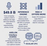
With over 500 million smart speakers already in homes and a voice assistant application market projected to grow from $6.3 billion in 2025 to $49.82 billion by 2033, the future of voice computing is moving from cloud to edge.[2] On-device processing for wake-word detection, keyword spotting, and natural language understanding is becoming the standard.

This shift to local inference brings critical benefits: improved responsiveness, enhanced user privacy, and lower ongoing cloud infrastructure costs. [3] But it also creates a new dilemma for chip architects: how to bring data center-grade inference capability into a consumer SoC with a bill of materials often constrained to under $3–$10 per unit, depending on the device class. [4]

That challenge is reshaping SoC architecture. [5] These devices must now deliver real-time performance, neural inference, and ultra-low power consumption in thermal and cost envelopes more typical of smart remotes than smartphones.

A $10–$15 Billion Opportunity

While high-end smartphones can afford complex neural engines, the majority of voice-enabled products—like thermostats, remotes, and earbuds—cannot. These devices require purpose-built, cost-efficient SoCs priced in the $3–$10 range. According to Market.us, the edge AI integrated circuits (ICs) market is projected to grow from $17.3 billion in 2024 to $340.2 billion by 2034, with over 70% of that value attributed to inference tasks—including those performed by voice-optimized SoCs for wake-word detection, on-device speech recognition, and natural language processing (NLP). [6]

The SoC as the Voice Compute Backbone

To support always-on voice capabilities, SoCs must become the central compute engine inside embedded devices. These chips must continuously listen for user input while consuming only milliwatts of power. They need to execute inference tasks, such as wake-word recognition and intent parsing, in less than 100 milliseconds. They also must interface seamlessly with control logic and input/output systems, all while adhering to strict cost constraints—typically with a bill of materials under $10.

This shift reflects a broader trend toward embedding intelligence directly into the fabric of everyday products. Consumers don’t expect to buy separate “voice assistants.” They expect voice interaction to be built in and invisible—like buttons or touchscreens once were.

SoC Design for Voice as a Feature

Meeting these requirements calls for a hybrid SoC architecture. This includes a scalar processor—typically ARM or RISC-V—for managing operating system tasks and control logic. [7] A vector or matrix engine handles the heavy lifting of AI tasks such as wake-word detection and intent parsing. To ensure efficiency and predictability, the architecture incorporates a deterministic scheduling model that avoids the power and verification challenges of speculative execution.

This combination delivers advanced AI workloads efficiently—without the thermal and architectural overhead of traditional, general-purpose designs.

In this new generation of voice-enabled devices, the vector-matrix processor is not just more valuable than the scalar unit—it is the performance and power bottleneck driver. Inference workloads such as wake-word detection, keyword spotting, noise suppression, and intent parsing now account for over 80% of total compute cycles and up to 90% of dynamic power consumption in voice-capable SoCs.

The AI engine typically occupies 2–3× the silicon area of the scalar core, yet delivers orders of magnitude higher throughput per watt. [8]

A Next-Generation SoC Axelon Interface Integrates Scalar & Vector

Simplex Micro’s Axelon architecture embodies this next-gen approach. It provides a flexible CPU interface to integrate a scalar core (ARM or RISC-V) with a RISC-V Vector engine, while introducing a novel time-based execution model. This deterministic scheduler eliminates the complexity of speculative execution—a common technique in general-purpose CPUs that adds power and verification overhead—delivering consistent, low-latency AI performance.

ARM vs. RISC-V: The Battle for AI Acceleration

ARM continues to dominate the scalar core market and will remain a cornerstone for control logic. However, when it comes to AI acceleration, ARM’s Neon SIMD architecture is limited in vector width, scalability, and power efficiency.

In contrast, RISC-V—with its open architecture, variable-length vector support, and extensibility for custom AI instructions—offers a more scalable and energy-efficient foundation for edge inference. These advantages are driving its adoption in hybrid SoCs optimized for embedded voice.

Conclusion: Voice Is Infrastructure, Not a Product

We are witnessing a silent revolution in silicon. Voice is no longer a standalone product category—it’s infrastructure. A baseline feature, embedded directly into the interface layer of modern devices.

The companies designing the SoCs that enable this transition will define the next generation of user interaction. ARM will remain essential for control, but the competitive frontier is in AI acceleration. Here, RISC-V vector processors—especially when paired with deterministic execution models like Simplex Micro’s Axelon—are poised to lead. Quietly and efficiently, they are powering the age of voice as a feature.

References

[1] Remesh. (2022). 5 Ways Voice Recognition Technology Sways Consumer Buying Behavior. https://www.remesh.ai/resources/voice-recognition-technology-consumer-buying-behavior

[2] MarketsandMarkets. (2024). Voice Assistant Application Market Size. https://www.marketsandmarkets.com/Market-Reports/voice-assistant-application-market-1235279.html

[3] ARM. (2025). Silicon Reimagined Report. Chapter 2: AI at the Edge. https://www.arm.com/company/newsroom

[4] ARM. (2025). Silicon Reimagined Report. Chapter 2: Power-efficiency limits. https://www.arm.com/company/newsroom

[5] ARM. (2025). Silicon Reimagined Report. Chapter 1: Custom silicon trends. https://www.arm.com/company/newsroom

[6] Global Edge AI ICs Market Size, Share, Statistics Analysis Report By Chipset  https://market.us/report/edge-ai-ics-market/

[7] ARM. (2025). Silicon Reimagined Report. Chapter 2: Vector/matrix specialization. https://www.arm.com/company/newsroom

[8] Patel, D. (2022). Apple M2 Die Shot and Architecture Analysis – Big Cost Increase for Minor Performance Gains. SemiAnalysis. https://www.semianalysis.com/p/apple-m2-die-shot-and-architecture

Also Read:

S2C: Empowering Smarter Futures with Arm-Based Solutions

SystemReady Certified: Ensuring Effortless Out-of-the-Box Arm Processor Deployments

The RISC-V and Open-Source Functional Verification Challenge


From All-in-One IP to Cervell™: How Semidynamics Reimagined AI Compute with RISC-V

From All-in-One IP to Cervell™: How Semidynamics Reimagined AI Compute with RISC-V
by Kalar Rajendiran on 05-26-2025 at 6:00 am

Started with a look at CPU

In an era where artificial intelligence workloads are growing in scale, complexity, and diversity, chipmakers are facing increasing pressure to deliver solutions that are not only fast, but also flexible and programmable. Semidynamics recently announced Cervell™, a fully programmable Neural Processing Unit (NPU) designed to handle scalable AI compute from the edge to the datacenter. Cervell represents a fundamental shift in how AI processors are conceived and deployed. It is the culmination of Semidynamics’ IP offerings evolution from modular IP components to a tightly integrated, unified architecture, rooted in the open RISC-V ecosystem.

The Roots of Cervell: A Modular Foundation

Cervell’s architectural DNA can be traced to Semidynamics’ earlier innovations in customizable processor components. The company began by developing highly configurable 64-bit RISC-V CPU cores that allowed customers to tailor logic and instruction sets to their unique requirements. These cores served as the foundation for control flow and orchestration in AI and data-intensive systems.

As AI workloads evolved, Semidynamics introduced vector and tensor units to extend the performance of its RISC-V platforms. The vector unit enabled efficient parallel processing across large data sets, making it well-suited for signal processing and inference tasks. Meanwhile, the tensor unit brought native support for matrix-heavy computations, such as those central to deep learning. Importantly, both units were designed to share the same register file and memory system, reducing latency and improving integration.

These components formed the basis of what the company called its “All-in-One” IP architecture—a modular approach that gave chip designers the freedom to assemble compute units tailored to their application. However, it still required developers to integrate, manage, and orchestrate these units at the system level. Cervell changes that.

Why Semidynamics Chose to Build an Integrated NPU

As AI models became larger and more complex, the need for a more unified compute platform became clear. Traditional approaches—where CPUs handle orchestration and discrete accelerators handle AI inference—were increasingly hindered by memory bottlenecks, data movement latency, and software complexity. Fragmented architectures that required separate cores for control, vector operations, and tensor math no longer met the performance and efficiency demands of modern AI workloads.

Moreover, as customers began to prioritize programmability and long-term flexibility, it was evident that an off-the-shelf NPU with fixed functionality would no longer suffice. Semidynamics saw the opportunity to converge its modular IP blocks into a single, coherent compute architecture. Cervell is a RISC-V NPU that is not only scalable and programmable, but also capable of eliminating the need for fallback or offload operations.

A New Category of NPU: Coherent, Programmable, and Scalable

What distinguishes Cervell from traditional NPUs is its unification of compute components under one roof. Rather than treating the CPU, vector unit, and tensor engine as separate blocks requiring coordination, Cervell integrates all three within a single processing entity. Each element operates within a shared, coherent memory model, meaning data flows seamlessly between control logic, vector processing, and matrix operations without needing DMA transfers or synchronization barriers.

This integration enables Cervell to execute a full range of AI tasks without falling back to an external CPU. Tasks that traditionally caused performance bottlenecks—such as control flow in transformer models or non-linear functions in recommendation engines—are now handled within the same core. With support for up to 256 TOPS in its highest configuration, Cervell achieves datacenter-level inference performance while remaining flexible enough for low-power edge deployments.

Cervell’s Market Impact

By removing the artificial boundaries between compute types, Cervell delivers a simplified software stack and more predictable performance for AI developers. Its design challenges the status quo of traditional NPUs, which often rely on closed, fixed-function pipelines and suffer from limited configurability. In contrast, Cervell empowers companies to tailor the architecture to their algorithms, allowing for truly differentiated solutions.

The Role of RISC-V in Enabling the Cervell Vision

None of this would be possible without the open RISC-V instruction set architecture. RISC-V allows developers and chip designers to deeply customize the ISA, add proprietary instructions, and maintain compatibility with open software ecosystems. In the case of Cervell, RISC-V serves not only as a technical enabler, but as a strategic differentiator.

Unlike proprietary ISAs that limit innovation to a vendor’s roadmap, RISC-V allows Cervell’s capabilities to evolve alongside customer needs. The openness of RISC-V means companies can build processors that match their business and technical requirements without being locked into closed ecosystems. This flexibility is crucial in AI, where workloads shift quickly and the ability to adapt can be a competitive advantage.

Cervell vs. Semidynamics’ Earlier All-in-One IP

While the All-in-One IP architecture laid the groundwork for what Cervell has become, the differences are profound. Previously, customers had to select and integrate CPU, vector, and tensor components on their own, often dealing with toolchain and memory integration complexity. Cervell consolidates these elements into a pre-integrated NPU that is ready to deploy and scale.

Cervell is a holistic product that includes a coherent memory subsystem, programmable logic across all compute tiers, and a software-ready interface supporting common AI frameworks. Furthermore, Cervell introduces performance scaling configurations, from C8 to C64, ensuring the same architecture can serve everything from ultra-low-power IoT devices to multi-rack datacenter inference systems.

Summary: The Future of Scalable AI Compute

Cervell brings together programmability, performance, flexibility and scalability to AI solutions. By building on RISC-V and eliminating the barriers between CPU, vector, and tensor processing, Semidynamics has delivered a unified architecture that scales elegantly across deployment tiers.

Cervell is a trademark of Semidynamics. Learn more at Cervell product page.

Also Read:

Andes RISC-V CON in Silicon Valley Overview

Keysom and Chipflow discuss the Future of RISC-V in Automotive: Progress, Challenges, and What’s Next

Vision-Language Models (VLM) – the next big thing in AI?


Executive Interview with Mohan Iyer – Vice President and General Manager, Semiconductor Business Unit, Thermo Fisher Scientific

Executive Interview with Mohan Iyer – Vice President and General Manager, Semiconductor Business Unit, Thermo Fisher Scientific
by Daniel Nenni on 05-24-2025 at 10:00 am

MohanPicWorkday 11302021

Mohan Iyer serves as the Vice President and General Manager of the Semiconductor Business Unit at Thermo Fisher Scientific, a global leader in providing reference metrology, defect characterization, and localization equipment. These advanced systems are essential for driving innovation, accelerating time to market, and optimizing manufacturing yields in the semiconductor industry. Mohan has over 27 years of experience in the semiconductor industry specializing in semiconductor equipment and process control.

Tell us about your company?

Thermo Fisher Scientific’s mission is to enable our customers to make the world healthier, cleaner and safer. Our life sciences solutions, specialty diagnostics, analytical instruments and laboratory, pharmaceutical and clinical research services help improve patient health, increase productivity in laboratories, develop and manufacture life-changing therapies, help solve complex analytical challenges and support cleaner environments.

Through our extensive capabilities and global reach, we empower our customers to accelerate breakthroughs in scientific discovery, human health, global sustainability and safety. Today, technological advancements are powering our modern world – from new materials for cleaner energy solutions to advanced semiconductors that make way for next-generation technologies like artificial intelligence and machine learning. The recent launch of the Thermo Scientific Vulcan™ Automated Lab, a solution that will drive a new era of process development and control in semiconductor manufacturing, supports the growing global need for analytical instruments and expertise within the semiconductor manufacturing industry.

What problems are you solving?

Thermo Fisher Scientific addresses key challenges in the semiconductor industry by providing solutions across R&D, yield management, and failure analysis. In R&D, our state-of-the-art atomic-scale imaging, elemental analysis, and characterization capabilities enable the development of high-performance materials and the precise structural innovations necessary for next-generation semiconductor devices. Furthermore, we offer precision circuit-editing technologies that accelerate the prototyping of new devices, significantly reducing mask costs and enabling faster time-to-market. In yield management, our metrology solutions support in-line metrology correlations, allowing semiconductor manufacturers to resolve yield excursions. In failure analysis, our defect analysis workflows provide rapid and accurate root cause analysis of manufacturing defects or customer returns.  Our electrostatic discharge test systems ensure compliance with industry standards, safeguarding the reliability and performance of semiconductor devices. These advanced solutions help optimize the semiconductor manufacturing process, driving innovation, reducing costs, and improving product quality across the industry.

What application areas are your strongest?

Our strongest application areas are centered around defect characterization and metrology in semiconductor manufacturing using failure analysis instruments, Scanning Electron Microscopy (SEM), Focused Ion Beam (FIB), and TEM (Transmission Electron Microscopy).  We specialize in our ability to ‘see the unseen’.   As industry defect tolerance has shifted from parts per million to parts per billion, it’s crucial to identify defects quickly and accurately. This is especially important with AI chips, where latent defects are an increasing concern. We excel at accurately localizing defects for failure analysis and can quickly characterize these defects using chemical analysis and other electron microscopy methods. Additionally, we help control development and manufacturing processes in the fab by providing precise metrology for structures buried beneath the wafer surface.

We have decades of experience in developing automated workflows that significantly improve our customers’ productivity. Ultimately, we deliver comprehensive, atomic-scale data solutions with the highest level of automation, leveraging our cutting-edge instruments to meet the demands of the semiconductor industry.

What keeps your customers up at night?

As consumer products require more powerful computing capabilities, defect rates in chip development naturally rise with new technologies. A subtle defect that was previously in the ‘noise’, is now causing issues and they need to find those very subtle defects. A prime example is the rapid adoption of AI across various industries, which drives the need for even more sophisticated chips. A critical defect or process issue in the fab can severely delay time to market, which is a major concern for our customers. They need these issues identified and resolved quickly to maintain competitive advantage. Additionally, as advanced chips become more expensive to produce, managing operational costs becomes even more important. Our customers need automated workflows to reduce the burden on operators and streamline processes, helping to control costs while maintaining quality and speed. By addressing these challenges, we help them stay ahead in a rapidly evolving industry.

What does the competitive landscape look like and how do you differentiate?

The competitive landscape in electron microscopy is established with other vendors providing instruments in this space.  However, we differentiate by offering advanced solutions that are increasingly critical as device structures shrink and become more complex. Our exceptional ability to precisely localize defects, reveal them for analysis, and provide atomic-scale resolution imaging is essential for meeting the industry’s evolving needs. Furthermore, what sets us apart is our unique automated workflows, which streamline analysis throughout the entire semiconductor product development cycle. By leveraging our deep hardware expertise, software integration, and AI innovations, we help our customers boost productivity and reduce time to market. Additionally, we stand out by having a dedicated semiconductor market division, focused exclusively on providing instruments and workflow solutions tailored to the industry’s needs. With decades of experience in providing specialized service and applications support, we’ve built a strong reputation for being the go-to partner for the semiconductor market. This combination of cutting-edge technology, market focus, and customer support is what truly differentiates us in the competitive landscape.

What new features/technology are you working on?

We’re continuously working on developing higher precision instruments to characterize even smaller structures. As chip devices become more complex, our goal is to ‘see the unseen’ by advancing both hardware and specialized software capabilities.  For example, in defect localization applications, instead of using traditional optical imaging we’ve integrated a high resolution SEM into the Meridian EX system, resulting in a remarkable improvement in probing precision.  Additionally, as chip footprints shrink and devices are stacked vertically, this introduces challenges in revealing structures that are microns, or even hundreds of microns, below the wafer surface. This drives us to continue our innovations in precisely revealing defects and generating metrology data for these cutting-edge chips. Another exciting focus is bridging the lab-to-fab time to data gap. We’re expanding automation not just within our instruments but also integrating our automation systems with those in the lab and fab. Our Vulcan Automated Lab is a great example. This will significantly streamline processes and reduce the time it takes to get actionable data, ultimately boosting efficiency and productivity in semiconductor manufacturing

How do customers normally engage with your company?

Our customers typically engage with us through various channels to ensure we meet their needs. One key method is through technical review meetings, where we share roadmaps and ensure we’re developing targeted solutions. We also interact with customers through seminars, conferences, and webinars. Engaging with our customers is crucial to our shared success, and we host and attend numerous events throughout the year.

Additionally, as mentioned earlier, we pride ourselves on providing strong local sales, service, and application support. Our extensive network of semiconductor-focused engineers, located worldwide, works closely with customers to address their specific challenges. We also use our global demo labs, called NanoPorts, as a way for customers to engage with us in solving cutting-edge problems and evaluating new technologies and techniques.

These interactions not only allow us to showcase our latest innovations but also give us the opportunity to learn directly from customers, ensuring we understand their current and future challenges. This two-way communication is key to our ability to provide effective, forward-thinking solutions.

Also Read:

CEO Interview with Jason Lynch of Equal1

CEO Interview with Sébastien Dauvé of CEA-Leti

CEO Interview with Sudhanshu Misra of ChEmpower Corporation


CEO Interview with Jason Lynch of Equal1

CEO Interview with Jason Lynch of Equal1
by Daniel Nenni on 05-24-2025 at 6:00 am

Equal1. 27/2/25 Picture by Fergal Phillips

For more than 20 years, Jason has delivered high impact results in executive management. Prior to Equal1, he held several executive management positions at Analog Devices, Hittite and Farren Technology. In these roles, Jason built and managed large teams comprising sales, operation and finance and was responsible for significant revenue targets. He also drove AI for predictive maintenance, made Internet of Things (IoT) a reality, using cutting-edge sensors and Artificial Intelligence (AI) to save factory-owners millions of dollars in unplanned downtime.

Tell us about your company.

Equal1 is a global leader in silicon-based quantum computing. With a world-class team spanning Ireland, the US, Canada, Romania, and the Netherlands, we are focused on building the future of scalable quantum computing through our patented Quantum System-on-Chip (QSoC) technology.

Our UnityQ architecture is the world’s first hybrid quantum-classical chip, integrating all components of a quantum computer onto a single piece of silicon. This breakthrough enables cost-effective, energy-efficient quantum computing in a compact, rack-mountable form, ready for deployment in existing data center infrastructure.

Our approach radically reduces the size and cost of quantum systems, preparing them to unlock real-world applications across sectors such as pharmaceuticals and finance.

Our first commercial product, the Bell-1 Quantum Server, is now shipping to customers worldwide.

What problems are you solving?

Quantum computing today faces two major barriers – scalability and deployability. Most current systems are bulky, power-hungry and confined to lab environments, making them impractical for real-world adoption.

At Equal1 we’re solving this by delivering a fully integrated, silicon-based quantum computing platform that is compact, energy-efficient and manufacturable using standard semiconductor processes. Our UnityQ QSoC architecture eliminates the need for complex infrastructure, enabling quantum computing to be deployed in existing data centers and HPC environments.

We’re also addressing the challenge of hybrid processing by embedding quantum and classical components on a single chip. This allows for real-time quantum-classical interaction, which is a critical capability for solving complex problems in data-sensitive sectors like pharmaceuticals and finance.

What application areas are your strongest?

Our technology is designed for application areas where quantum-classical hybrid computing has the potential to deliver significant future impact. While commercial applications are still in early stages industry-wide, our QSoC platform is especially well-positioned to support:

  • Pharmaceuticals: simulating molecular interactions and accelerating early-stage drug discovery.
  • Finance: exploring advanced optimisation and risk modelling techniques.
  • Data centre efficiency: enabling more energy-efficient computation and reducing the environmental footprint of large-scale infrastructure.

These sectors share common characteristics of data intensity, high computational complexity and sensitivity, making them prime areas for early hybrid quantum-classical exploration. Equal1’s compact, energy-efficient systems are built to integrate easily into existing infrastructure, enabling customers to prepare for and experiment with quantum workloads today.

What keeps your customers up at night?

Our customers – along with many closely watching the evolution of quantum computing – are excited about the promise of the transformative technology, but they also have uncertainty about when and how that transformation will take place. There are differing views on when quantum computing will begin to deliver real-world value, and how quantum systems will fit into existing operations. Many current quantum solutions are far from enterprise-ready. For organisations in highly regulated, data-sensitive industries like finance and pharmaceuticals, the stakes are even higher.

At Equal1, we’re taking a grounded, practical approach. We see quantum not as a replacement for classical computing, but as a complement – an accelerator within high-performance computing environments. And importantly, quantum is scaling faster than classical computing ever did, bringing us closer to practical applications than many once thought possible.

What does the competitive landscape look like and how do you differentiate?

The quantum computing space is full of exciting and diverse approaches, but what makes Equal1 stand out is our focus on silicon-based quantum technology. We’re proud to be the first company to launch a silicon-based quantum server, Bell-1 – a compact, rack-mounted system designed for deployment in real-world data centers.

We’ve also recently achieved a major milestone by validating a commercial CMOS process for quantum devices. This proves that quantum computing can be built using the same mature, scalable technology behind classical semiconductors, paving the way for what we call Quantum 2.0: practical, integrated and ready to scale. While others are still working with complex, custom platforms, we’re focused on delivering quantum solutions that fit into today’s data centers and tomorrow’s high-performance computing infrastructure.

What new features/technology are you working on?

We’re focused on pushing the boundaries of what’s possible with our silicon-based architecture. Our UnityQ Quantum System on Chip Processor roadmap will deliver millions of physical qubits, uniting quantum and classical components on a single chip using commercial semiconductor manufacturing processes.

To bring these next-generation capabilities to life, we’re working closely with industry and research partners who share our vision for practical, scalable quantum computing. These collaborations are critical in helping us accelerate development and ensure our technology addresses real-world needs from day one. We’re very excited for what’s to come for Equal1.

Visit our website at equal1.com.

Also Read:

CEO Interview with Sébastien Dauvé of CEA-Leti

CEO Interview with Sudhanshu Misra of ChEmpower Corporation

CEO Interview with Thar Casey of AmberSemi


Podcast EP288: How Alphawave Semi Enables Next Generation Connectivity with Bharat Tailor

Podcast EP288: How Alphawave Semi Enables Next Generation Connectivity with Bharat Tailor
by Daniel Nenni on 05-23-2025 at 10:00 am

Dan is joined by Bharat Tailor who is responsible for the Alphawave standard connectivity products portfolio focused on DSP chipsets enabling AI data center interconnects. He is a veteran of the high-speed connectivity semiconductor industry having participated in the evolution of connectivity technologies from 10Gbps to the current discussions on 3.2T and beyond.

Dan explores the many demands of high speed, high density and low power connectivity with Bharat. Driven by ever-growing AI deployment, Bahrat explains some of the many constraints that must be met for next generation systems. He describes Alphawave’s move to a semiconductor supplier and how that has facilitated a very broad product portfolio to address the many needs ahead.

He describes how Alphawave’s silicon IP, chiplets, custom silicon and connectivity products work together to address the demands of applications such as those found in hyperscale data centers. He explains that three of four engagements are now focused on chip delivery at Alphawave Semi. Baraht also discusses the path to 448 Gpbs channels and some of the technical problems that must be solved.

The views, thoughts, and opinions expressed in these podcasts belong solely to the speaker, and not to the speaker’s employer, organization, committee or any other group or individual.

Contact Alphawave


Video EP6: The Benefits of AI Agents for Waveform Debugging with Zackary Glazewski of Alpha Design

Video EP6: The Benefits of AI Agents for Waveform Debugging with Zackary Glazewski of Alpha Design
by Daniel Nenni on 05-23-2025 at 6:00 am

In this episode of the Semiconductor Insiders video series, Dan is joined by Zackary Glazewski, an ML Engineer at Alpha Design AI. Dan explores the challenges of waveform debugging with Zack, who explains how the process is done today and the shortcoming of existing approaches. He explains why current approaches are time consuming and error-prone. A key required element is linking observed waveform behavior to the actual circuit to find the real issue. Zack describes how Alpha Design AI’s unique AI Agents address these challenges.

The views, thoughts, and opinions expressed in these videos belong solely to the speaker, and not to the speaker’s employer, organization, committee or any other group or individual.


Infinisim Enables a Path to Greater Profitability and a Competitive Edge

Infinisim Enables a Path to Greater Profitability and a Competitive Edge
by Mike Gianfagna on 05-22-2025 at 10:00 am

Infinisim Enables a Path to Greater Profitability and a Competitive Edge

Improved profitability and competitiveness are at the very heart of every enterprise. Achievements like this are usually attributed to corporate culture. Sometimes, it’s just being in the right place at the right time. Some organizations make huge investments with top-tier consulting companies to help find their way.

Recently Infinisim published a white paper about clock jitter, why it’s a problem and how to minimize its effects. One would expect this kind of information to help with first-time silicon success, and it does. But the white paper also explains how a good clocking strategy will pave the way to broader corporate success. A link is coming for this important white paper but first let’s examine how Infinisim enables a path to greater profitability and a competitive edge.

The Technology Story

Decreasing supply voltages and increasing operating frequencies create substantial design challenges. As the stakes go up and the margins become smaller, challenges that were once manageable now pose significant risks for performance, yield, and long-term reliability. In the middle of all this is a subtle but significant disruptor: clock jitter.

Clock jitter refers to the deviation of a clock signal from its ideal timing. In digital systems, clocks are essential for synchronizing operations and ensuring reliable logic propagation. Even minor variations can lead to timing violations and catastrophic failures in high-performance designs. This white paper explains the various contributors to clock jitter. They include timing variations from the PLL and the power delivery network (PDN). PDN induced jitter is the larger problem as it can vary all over the chip.

The ways this happens, and the implications are explained in detail. The main impacts of clock jitter include slower chip performance and lower yield. More on these effects in a moment.

The white paper also explains why traditional solutions to managing clock jitter fall short. A lot of detail and analysis is shared here. The fundamental point is that finding and managing clock jitter with conventional tools is impractical. Detailed SPICE-level accuracy is needed across many, many scenarios. There is simply not enough time to do the work needed with the required accuracy in a typical design schedule.

And so, the answer to this problem has been to develop design margins. If the team stays within these margins, the chances of catastrophic timing variation due to clock jitter is low.  But, as they say, there is no free lunch. As more advanced technology puts higher demands on performance and timing, design margins tend to grow to the point where substantial compromises are made. This is the second part of the story.

The Business Story

The white paper explores several ways clock jitter impacts the overall competitiveness and profitability of an enterprise. An analysis is offered that explores what happens to the lifetime profitability of a design when clock jitter creeps in. You will be able to see to the details, but the overall impact is measured in millions of dollars.

Expanding design margins are also discussed. Overly pessimistic design margins leave performance and profitability on the table. Impacts include lower speed, resulting in a lack of competitiveness and lost market share. Paying high fees for advanced technology and not using all its capabilities also impacts the bottom line. The white paper offers many details that are important to consider.

Solving clock jitter with new technology is a major focus of Infinisim. The company is the industry leader in SoC clock verification for high-performance designs. At advanced process nodes, where nanometer-scale effects dominate, Infinisim enables design teams to push clock performance further than traditional tools can reach. The white paper goes into the details of how Infinisim’s platform delivers game-changing technology, opening up greater profitability and competitiveness.

You will be able to read all the details in the white paper. Below is a graphic that provide a high-level view of the capabilities Infinisim’s platform delivers. 

Infinisim’s Comprehensive Clock Solution

To Learn More

I’ve just provided a high-level overview of what this new white paper from Infinisim offers. There is much more to learn. If improved competitiveness and profitability appeal to you, you need to get your own copy of this white paper.

You can request a copy of the white paper here. And that’s how Infinisim enables a path to greater profitability and a competitive edge.

Also Read:

2025 Outlook with Samia Rashid of Infinisim

My Conversation with Infinisim – Why Good Enough Isn’t Enough

The Perils of Aging, From a Semiconductor Device Perspective


Andes Technology: A RISC-V Powerhouse Driving Innovation in CPU IP

Andes Technology: A RISC-V Powerhouse Driving Innovation in CPU IP
by Kalar Rajendiran on 05-22-2025 at 6:00 am

Celebrate Andes 20 Years Anniversary

As it celebrates its 20th anniversary in 2025, Andes Technology stands as a defining force in the RISC-V movement—an open computing revolution. What began in 2005 as a bold vision to deliver high-efficiency Reduced Instruction Set Computing (RISC) processor IP has evolved into a company whose innovations power billions of devices worldwide. And Andes’ impact extends well beyond hardware. Through sustained investment in open-source software and active leadership in industry initiatives, the company has played a key role in strengthening the RISC-V ecosystem and ensuring seamless integration between architecture and software.

Frankwell Lin, Chairman and CEO of Andes Technology gave a keynote presentation at Andes RISC-V CON 2025. This annual conference, convened by Andes, has grown steadily in both attendance and speaker participation since its inception, reflecting the company’s increasing market adoption and growing influence on the technology front. The following is a synthesis of Lin’s talk.

Early Commitment to RISC-V

From the outset, Andes focused on delivering high-efficiency CPU IP based on the RISC philosophy. Its proprietary AndeStar™ ISA and development platform, AndeSight™ IDE, formed the technological bedrock for its early success, offering customers a flexible and scalable foundation for SoC design.

In 2016, Andes became a founding member of RISC-V International, well before the open ISA gained mainstream industry momentum. That same year, it was recognized by TSMC with a “New Partner of the Year” award, signaling the broader ecosystem’s confidence in Andes’ direction.

By 2018, Andes had crossed the threshold of one billion SoCs shipped with its CPU IP embedded. The company has since shipped more than 16 billion chips through its customers’ designs, with over two billion units delivered in 2024 alone.

From Innovation to Market Leadership

Andes introduced its first RISC-V processor IP in 2017, marking the beginning of a wave of technical innovation. It soon followed up with the industry’s first RISC-V Packed-SIMD CPU. The NX27V, the first commercially available RISC-V Vector CPU IP was adopted by Meta shortly after the IP was launched in 2019. These breakthroughs demonstrated that RISC-V could address high-performance computing needs as effectively as proprietary architectures.

The company’s momentum continued with the release of ISO 26262–compliant safety cores in 2022, followed by a multicore vector processor in 2023. In 2024, Andes became the first to introduce a RISC-V processor compliant with ISO 26262’s stringent ASIL-D safety requirements.

Today, Andes operates on a predictable release cadence, launching six new RISC-V cores each year to meet the needs of markets from AI to automotive. You can read about Andes full lineup of RISC-V processor solutions on a separate post on SemiWiki.

Establishing RISC-V Standards: RVA23 and Beyond

Beyond its product offerings, Andes plays a leading role in the governance and evolution of the RISC-V ISA. As a member of the Board of Directors and Technical Steering Committee at RISC-V International, the company has helped shape major architecture extensions, including packed SIMD, matrix multiplication, fast interrupt handling, and IOPMP for memory protection.

A significant part of Andes’ commitment to standardization is its full alignment with the RVA23 profile, the recently ratified standard that defines a consistent set of features for 64-bit RISC-V application processors. This profile mandates support for key extensions such as vectors and virtualization, helping ensure consistency across platforms. Andes has already incorporated RVA23 compliance into its roadmap, further cementing its position as a leader in forward-compatible, ecosystem-ready processor IP.

Building the Software Foundation

Understanding that hardware alone isn’t enough, Andes has long invested in enabling software. The company is an active contributor and maintainer of several core open-source projects, including GCC, glibc, Linux, U-Boot, and SIMDe. It also supports broader ecosystem efforts through involvement in the RISE project, the Linux Foundation, and the Civil Infrastructure Platform, all aiming to strengthen RISC-V software infrastructure.

By engaging deeply with both the hardware and software layers, Andes ensures that its IP not only meets performance and power goals but also integrates seamlessly into modern toolchains and operating systems.

Sustained Growth and Global Reach

Following its IPO in 2017, Andes has delivered consistent growth with a compound annual revenue growth rate of 26.8 percent. In 2024, it recorded an impressive 30.6 percent growth—largely fueled by RISC-V, which now accounts for 92 percent of its license revenue. The company has signed more than 200 RISC-V commercial license agreements and operates six global design centers, supporting customers across North America, Asia, and Europe. It is the global market leader in RISC-V IP, with over 30% market share, as reported by market research firm, The SHD Group.

A New Identity for a New Era

In April 2025, Andes Technology unveiled a refreshed corporate logo as part of its 20th-anniversary celebrations. The new logo represents the company’s evolution and its commitment to innovation in the RISC-V ecosystem. The “S” in the new logo, stylized as a “5” reflects its alignment to the RISC-V open-standard movement. Alongside the rebranding, Andes announced the expansion of its headquarters, signaling its continued growth and dedication to serving a global customer base.

Looking Ahead: Innovation with Focus

Andes is a pure-play CPU IP provider with a broad impact across the semiconductor landscape. With deep engagement in safety-certified applications, artificial intelligence, and cloud-edge computing convergence, the company is well poised to shape the future of RISC-V in markets that demand both performance and trust.

To learn more, visit Andes website.

Also Read:

Andes RISC-V CON in Silicon Valley Overview

Webinar: Unlocking Next-Generation Performance for CNNs on RISC-V CPUs

Relationships with IP Vendors


CEO Interview with Sébastien Dauvé of CEA-Leti

CEO Interview with Sébastien Dauvé of CEA-Leti
by Daniel Nenni on 05-21-2025 at 10:00 am

CEA024122 MOREL CEABD (1)

Sébastien Dauvé has been CEO of CEA-Leti since July 1, 2021. With over 20 years of experience in microelectronics and their applications—including clean mobility, future medicine, cybersecurity, and power electronics—he has played a key role in advancing digital innovation. A graduate of École Polytechnique and ISAE-SUPAERO, he began his career in defense radar systems before joining CEA-Leti in 2003. There, he led R&D activities in sensors, the Internet of Things, and system integration.

He has successfully designed and implemented strategies to accelerate technology transfer and support startup creation, always promoting cross-disciplinary collaboration to address key societal challenges through innovation. From sensors to wireless communications, his work focuses on combining energy efficiency with high performance to enable responsible, high-impact technological progress.

Tell us about your company?

Located in Europe’s deeptech hotspot of Grenoble, France, CEA-Leti has been pioneering innovation in micro and nanotechnologies since 1967. It is part of the CEA, a Clarivate Top 100 Global Innovator.

CEA-Leti’s model is designed to support companies throughout the innovation lifecycle. Companies of all types and sizes, from startups to major global corporations, have entered into long-term partnerships with CEA-Leti at various stages of their R&D journeys, from proof of concept to scaling new solutions up for volume manufacturing.

Today, CEA-Leti employs 2,000 people and boasts state-of-the-art technology platforms. These include clean rooms capable of processing 300 and 200 mm wafers.

What problems are you solving?

At CEA-Leti, we are addressing some of today’s most pressing technological and societal challenges by developing innovative solutions in microelectronics and nanotechnology. Expanding the “lab-to-fab” concept is at the heart of our mission — we accelerate the industrial adoption of cutting-edge technologies to strengthen Europe’s technological sovereignty. Our work goes beyond performance—we are increasingly placing sustainability at the core of innovation. By combining scientific excellence with a strong industry focus, we help shape a more responsible and competitive future for the tech sector.

What application areas are your strongest?

We are fortunate to master a number of technologies in which we have developed strong expertise, including photonics, healthcare technologies, quantum computing, sensors, advanced wireless communications and power electronics. This expertise enables us to prepare for longer-term technological breakthroughs, for example:

– Neuromorphic computing, in-memory computing and advanced FD-SOI technologies for high-performance, energy-efficient AI;

– Advanced chip-to-chip interconnections, leveraging photonics and heterogeneous integration to enable next-generation computing architectures;

– Miniaturization of systems for organs-on-a-chip, opening up new possibilities for personalized medicine and reducing reliance on animal experimentation.

In all cases, we are increasingly focused on developing solutions with a low environmental impact.

What does the competitive landscape look like and how do you differentiate?

Clearly, the semiconductor field is highly competitive and, above all, fast-paced in terms of innovation. There are only a handful of institutes at this level in the world, and it’s no coincidence that Europe has chosen us to be a key player in the European Chips Act. For over a year now, we have been coordinating a pilot line called FAMES, which has enabled us to expand our resources and, above all, to run large-scale programs for industry. This further strengthens our position.

But that’s still not quite enough. More than ever, we need to strengthen our ties and collaborations with other technological institutes and research centers. We share many common topics with our colleagues in fundamental research at the CEA, have numerous collaborations with CNRS, INRIA, IMT, etc. via the PEPR, and with many other European and even international RTOs. This capacity for collaboration is invaluable and truly enables us to remain at the cutting edge of technology.

Contact CEA-Leti

Also Read:

CEO Interview with Sudhanshu Misra of ChEmpower Corporation

CEO Interview with Thar Casey of AmberSemi

CEO Interview with Ido Bukspan of Pliops


Turnkey Multi-Protocol Wireless for Everyone

Turnkey Multi-Protocol Wireless for Everyone
by Bernard Murphy on 05-21-2025 at 6:00 am

CEVA spps min

There is no IoT without wireless. If you have a great idea for a world-beating IoT device, you must integrate a wireless module (Bluetooth, Zigbee, Wi-Fi, UWB…) into that device. A ready-made companion wireless chip connected to MCU is one approach but will significantly increase unit cost and reduce profits. Products in most IoT markets depend on System on Chips (SoC) with embedded wireless to meet cost and low power targets, a high barrier to entry for non-wireless experts. Prepackaged MAC & modem IP addresses part of the problem but not the RF part. Which is why a turnkey solution combining MAC, modem and RF is an important step to unleash a flood of new products from the great majority of potential innovators whose only shortcoming is lack of wireless expertise.

What new products?

If you want to sell billions of products, sell to consumers. It’s a tough market but differentiated products can be very successful. Wireless earbuds provide an obvious example. You might think that market has already been locked down but you’d be wrong. The Bluetooth SIG continues to innovate at a furious pace, now offering Auracast for unprecedented easy audio sharing experience, and introducing soon High Data Throughput (HDT) for even better audio quality with lossless multi-channel capability. Add 3D audio for a more realistic and immersive sound experience. In gaming, low latency improves the gaming experience whether through earbuds or headphones. Consider also that medical, payment, keyless entry, retail, hearing aid, and other applications build on the same low power Bluetooth communications links.

Meanwhile ZigBee, Thread and Matter, all underpinned by IEEE 802.15.4, are central to home automation. ZigBee is already well established for smart lights, smart thermostats and more. Thread and Matter are emerging options to extend interoperability between devices from various ecosystems. A smart home is likely to require support for some if not all these options and there are boundless opportunities to imagine more devices to further enhance convenience around the home.

Together the Bluetooth and 802.15.4 markets account for over $100B per year today and are expected to grow between 7% and 10% CAGR through 2029. This has to be a very appealing target for product builders.

Ceva-Waves Links200

If you have both wearables and home automation, you’re probably controlling them through your phone or tablet, maybe even your watch, all through either Bluetooth or 802.15.4. As a consumer you don’t care about protocols; you just want to turn on a light while listening to a playlist through your wireless earbuds. Which means that the wireless component in some of your devices must support all these options. Such multi-protocol support is not uncommon today, in some cases even adding Wi-Fi, cellular and UWB. Here, let’s focus on Bluetooth and 802.15.4.

Ceva pretty much owns the embedded Bluetooth business, providing solutions for many years and shipping over a billion devices per year. They stay very current with Bluetooth SIG releases, and even provide next generations ahead of official ratifications, now supporting up to Bluetooth 6.0 with LE Audio and Channel Sounding. They were also one of the first providers to qualify for Auracast compatibility. Next generations additions include low latency for gaming, High Data Throughput (HDT) that will more than triple the speed of traditional Bluetooth LE, allowing far better audio quality in Bluetooth LE than in Bluetooth Classic. The Links200 platform supports all of these capabilities, together with Bluetooth 6.0 Channel Sounding for accurate and secure ranging. The platform also provides IEEE 802.15.4 MAC support for ZigBee, Thread and Matter compliance and allows for concurrent multi-link communication through Ceva’s smart coexistence techniques.

All impressive but the big add in my view, to truly make this solution turnkey, is an included RF stage implemented in a TSMC 12nm FFC+ process for lower power, high performance (and low leakage). Equally important, this stage includes a class 1.5 power amplifier. All that is left for the integrator is to connect that output to an antenna. This unique turnkey IP platform is the only solution in the market enabling the design of innovative fully integrated Edge AIoT System on Chip with advanced processing power capability for headsets, earbuds, speakers, smart watches, smart glasses and more.

Integrating Links200

The Links200 IP is delivered with Verilog RTL source files for the digital part, C software source code running on the platform processor, and GDSII for the RF stage, plus a complete software framework to run on a host MCU. It also includes protocol stacks with comprehensive list of profiles to address a broad range of applications.

Ceva optionally supplies several complementary IPs to further enhance functionality, including:

  • The NeuPro-Nano, a unique Edge Neural Processor Unit IP that efficiently executes embedded ML workloads for always-on audio, voice, vision, and sensing use cases
  • RealSpace, a spatial audio software solution offering 3D audio rendering and low latency head tracking for gaming
  • ClearVox, a software solution for noise reduction and keyword spotting
  • MotionEngine, software solution for tap, in-ear detection and activity classification

You can read more about the Links200 capability HERE.

Also Read:

Ceva-XC21 and Ceva-XC23 DSPs: Advancing Wireless and Edge AI Processing

AI PC momentum building with business adoption anticipated

Bluetooth 6.0 Channel Sounding is Here