The announcement that Steve Ballmer will step down from Microsoft within the next 12 months and just weeks after kicking off a vast re-org focused on mobile devices can only mean that the future is coming much faster than Bill Gates or Steve Ballmer had ever expected and that without a radical adoption of hardware everywhere, it will leave the company without an existence (sans PC legacy) anywhere. The illness that effects Microsoft and Intel is a back to the future moment as the 30 year PC ecosystem dominance of Wintel will in the years to come likely be viewed as a radical departure from the traditional requirement that hardware and software co-existance is necessary in order to truly dominate. Thus the model of the IBM mainframe, the early Apple Mac and now the iphone/iOS platform shows that one ecosystem eventually dominates every generation, thus garnering more than 60% of the profits. We are way past the tipping point and Microsoft lacks ownership of hardware to drive its way forward. Be prepared for acquisitions such as Nokia as they aim for a comeback.
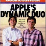
The mistake that Apple made, following the departure of Steve Jobs after the launch of the MAC was to rest on its high profit laurels. With what turned out to be a 10 year operating system lead, John Sculley had plenty of time to move Apple into a dominant position by building out a mid range and even entry level market in order to pull in the majority of the software world as Win 3.1 from Microsoft didn’t appear until 1992. And let’s not forget Microsoft held the O/S close enough to be the first to release the killer office applications. Only Lotus 1-2-3 and a few antiquated word processing apps gave the impetus for corporations to buy PCs in the 1980s. Think what might have been had Sculley acquired Lotus or incentivized them to come to market with a MAC version of 1-2-3 years before it appeared in 1991. A Mac selling for even $500 more than a PC but pre-installed with 1-2-3 would have driven the platform to dominance through the 1990s by the fact it would have won the highly prized corporate world.
Take note: Hardware Expensive, Software Free = Worldwide Dominance.
Back through history this has played out over and over and is now becoming the law of the land again. In the 1960s and 1970s, IBM sold expensive hardware with a bevy of free software and also expensive maintenance contracts. It would have carried over in the PC era if they had control of the hardware and the O/S. That minor detail shifted the profits to Intel and Microsoft or “Wintel.” However, Microsoft had the true upper hand as PC costs dropped by an order of magnitude from the original $5000 sticker price in 1981 until the beginning of this decade while they served up to corporate what it wanted most: the high priced “Office” productivity apps.
The latest earnings announcement from HP, which now has had its gross margins reduced to roughly 20%, is a sign that for even legacy to continue, Microsoft will have to take over the hardware business in order to guarantee that the razors get into the actual hands of users. Otherwise the razorblades sit on the shelf like outdated bananas. Intel is in a similar quandary on the client side and will ally themselves to the volume mobile manufacturers in order to guarantee volume for the fabs. Their true hope is that the rise of mobiles pushes more of the heavy lifting to the cloud where Xeon servers sell at a premium. Does Intel cheap mobile + expensive cloud servers mean increased revenue and profits? TBD
This past year and the coming months will truly test whether we are returning to an era of “expensive hardware and cheap software.” Apple has been severely tested by a mobile world inundated with cheap Android phones, some selling down to below $70. The market has shown over the past year that there is first and foremost a huge demand to move from feature phones to “internet phones.” Secondly, Apple has shown in test markets like India and the USA that when it moves the iphone into a midrange price point, the demand increases substantially. In addition it has increased its market share in enterprise to over 60% – does that number ring a bell?
Apple is at that 1985 moment again when Sculley decided to go for profits instead of following the Steve Jobs plan of figuring out how to sell a MAC to the masses and thereby capturing the dominant ecosystem position. Steve Jobs had wanted to price the original MAC down at $1000, however the hardware horsepower necessary to run the Operating System was more costly than first expected. Jobs knew however that Moore’s Law would be able to get him there within a couple turns of the crank and with the right roadmap they could have hustled to get there in the late 1980s.
If Apple is able to successfully lock down the midrange market with its new iPhone 5C, reportedly to be introduced on September 10[SUP]th[/SUP], than I expect that they will win the compute ecosystem of this generation. The cheap hardware, expensive software of the PC generation transitions to the “expensive hardware and cheap software” of the mobile generation. The ecosystem win will be underwritten by the corporate world, which demands standards and security and not by the worldwide masses of new mobile users who first enter at the thin margins.
lang: en_US