Synopsys IP Designs Edge AI 800x100

Altera, Intel, TSMC, ARM: the Plot Thickens

Altera, Intel, TSMC, ARM: the Plot Thickens
by Paul McLellan on 04-16-2013 at 7:15 pm

Vince Hu of Altera presented us her at the GlobalPress Electronics Summit on their process roadmap. Since just a month or two ago they announced that Intel would be their foundry at 14nm, everyone wanted to get a better idea of what was really going on.

At 28nm, Altera use 2 processes, TSMC 28HP (for high end Stratix-5 devices) and TSMC 28LP for mid-range, low-cost devices.


The next generation will use 3 processes. At 20nm their partner remains TSMC. TSMC’s 20nm is a planar process (FinFET starts at 14nm). At 14nm their foundry is Intel, with their TriGate process (their name for FinFET) which they will use for the highest performance devices. And they will also use TSMC’s 55nm process with embedded flash to make hybrid devices that are a bit like a PLD and a bit like and FPGA.

One interesting thing Vince said, just as an aside, was that 20nm will be lower power, higher performance and lower cost. Since there have been a lot of rumors that TSMC 20nm may not be cheaper than 28nm, that was an interesting datapoint. Altera will be announcing products here later this year.

So we started to ask questions.

Microprocessors? ARM is a great partner, at 20nm we are committed to ARM. What about 14nm? Is Intel going to manufacture ARM? Is Altera going to put Atoms on FPGAs? Too soon to comment but there may be an announcement soon. So my guess would be that Intel isn’t going to be building ARMs into Altera arrays and some sort of Altera/Intel processor deai will be announced in the future.

What about TSMC’s 14nm FinFET process? When that is available is Altera going to use it? Not discussing at this point.

How about 3D? TSV? Not ready to talk about it yet.

Vince, master of the cryptic remark, did say they are looking at what comes after, especially in the cost-sensitive space. They may even look at process technologies that are already out today. My guess would be that they might design lower cost arrays into 28nm once 28nm is no longer leading edge and wafer costs drop.

So FinFET is focused on Intel but they remain committed to TSMC. ARM is a strong partner but it remains to be seen what that means at 14nm. The future is a bit murky out there.


Webinar: Making a Simple, Structured and Efficient VHDL Testbench

Webinar: Making a Simple, Structured and Efficient VHDL Testbench
by Daniel Nenni on 04-16-2013 at 1:47 am

logo bitvis

Most simple testbenches have close to no structure, are terrible to modify and hopeless to understand. They often take far too much time to implement and provide close to no support when debugging potential problems. This webinar will demonstrate how to build a far better testbench with respect to all these issues – in significantly less time. The webinar will also explain how this verification approach results in reduced design and debug time with the help of an open-source testbench infrastructure library.

Guest Presenter: Espen Tallaksen, Bitvis CEO and Principal FPGA/ASIC Developer
[TABLE] cellpadding=”2″ cellspacing=”2″ style=”width: 90%”
|-
|
| Bitvis is a vendor independent Design Centre with competent designers, experienced in Embedded Software and FPGA/ASIC development and verification.
|-

Agenda

  • Making a verification specification
  • Defining your testbench architecture and concept
  • General testbench infrastructure library and methods
  • Implementing the testbench architecture
  • Implementing testcases

For more information, please visit http://www.aldec.com/events

Aldec Inc., headquartered in Henderson, Nevada, is an industry leader in Electronic Design Verification and offers a patented technology suite including: RTL Design, RTL Simulators, Hardware-Assisted Verification, SoC and ASIC Prototyping, Design Rule Checking, IP Cores, DO-254 Functional Verification and Military/Aerospace solutions.
www.aldec.com

lang: en_US


Variation-aware IC Design

Variation-aware IC Design
by Daniel Payne on 04-15-2013 at 4:18 pm

We’ve blogged before about Layout Dependent Effects (LDE) on SemiWiki and how it further complicates the IC design and layout process, especially at 28nm and lower nodes because the IC layout starts to change the MOS device performance. There’s an interesting webinarfrom Cadence on Variation-aware IC Design, created in December 2012, so I spent an hour today viewing it. Steven Lewis started out the webinar and then Alan Whittaker did a product demo showing how he uses Virtuoso to find and fix LDE issues.


Steve Lewis, Cadence
Continue reading “Variation-aware IC Design”


Chasing DP Rabbits

Chasing DP Rabbits
by SStalnaker on 04-15-2013 at 4:00 pm

“Now, here, you see, it takes all the running you can do, to keep in the same place. If you want to get somewhere else, you must run at least twice as fast as that!”
—Lewis Carroll, Through the Looking Glass

The use of stitching can greatly reduce the number of double patterning (DP) decomposition violations that a designer has to resolve. However, stitching also adds significantly increased complexity—the decomposition tool must process many additional design rules to generate legal stitches, and know how to use them properly during coloring. Despite these immense complexities, it has been possible to produce automated tool functionality that captures and applies all of these rules to produce successful layer decompositions.

Want to learn more about the intricacies of double/multi-patterning cut and stitch requirements and options? ReadDavid Abercrombie’s latest article for a thorough explanation, as well as specific strategies to avoid falling down the DP rabbit hole.

Too advanced? Maybe you need to start at the beginning (or know someone who does)? No problem, because we’ve complied all of David’s articles on double patterning in one place for your convenience. Amaze your friends and co-workers with your mastery of double patterning requirements and techniques!

lang: en_US


Two New TSMC-Cadence Webinars for Advanced Node Design

Two New TSMC-Cadence Webinars for Advanced Node Design
by Daniel Payne on 04-15-2013 at 3:43 pm

Foundries and EDA vendors are cooperating at increasing levels of technical intimacy as we head to the 20nm and lower nodes. Cadence has a strong position in the EDA tools used for IC design and layout of custom and AMS (Analog Mixed-Signal) designs. They have created a series of webinars to highlight the design challenges and new approaches required. In 10 days you can learn about addressing Layout-Dependent Effects (LDE) as part II. See my blog on the part I webinar.

Interested in advanced node designs? Enhance your expertise with two new webinars from TSMC and Cadence.


Continue reading “Two New TSMC-Cadence Webinars for Advanced Node Design”


Adam Osborne Pays Wintel a Visit

Adam Osborne Pays Wintel a Visit
by Ed McKernan on 04-14-2013 at 8:15 pm

The news this week that PC sales dropped by double digit percentages and to a level not seen since 2006 sent shudders down the halls of OEMs and chip suppliers. Are we entering a final death spiral as opposed to the gradual decline that most expected? Perhaps there is another explanation. From a distance, it appears that the mobile shift, not only caught Microsoft and Intel flat footed but also playing catch up with Marketing leading the way with “Futures.” The normally disciplined product rollouts have turned into a game of talking about game changing products and as a result the two companies are following the road Adam Osborne took 30 years ago. Corporations, meanwhile, are sitting on the sidelines waiting for the two to synchronize the platform. The longer this takes the greater the chance that Wintel unravels.

Before there was Michael Dell, there was Adam Osborne. In April 1981, Osborne launched the first commercially based portable computer, the Osborne 1 at $1795, which successfully ramped to 10,000 units a month. At the height of sales, in early 1983, he let it be known that two, new more advanced computers were on the way. Customers decided to wait and the rest as they say is history as sales dried up and bankruptcy ensued in the latter part of the year. Adam Osborne forever gained infamy in the realm of running a high tech company. The standard rule of thumb would be the phrase: “Don’t Osborne yourself.”

While many have predicted or wished the fall of Wintel, their more than 20 year run of success can be summarized as creating a standard and riding the diminishing returns of the components and margins of OEMs. As we entered this decade, the only two items that were left to be squeezed were the O/S and the processor. This steady state would have prevailed if not for the smartphone and tablet catalyst that offered entirely new platforms based on a cheap processor and “Free” O/S with Applications that were priced as low as $0.99.

Microsoft and Intel responded in a way that diminished each other and that of the combined platform that generates most of its sales and income with the business world. With Windows 8, Microsoft tried to extend the platform to operate on all PCs and mobiles while supporting x86 and ARM processors. It was a huge undertaking. Intel decided to pursue an O/S independent strategy with many of their internal engineers porting and optimizing Android to x86. To remain relevant in the mobile conversation dominated by Apple and Google, the two had to go public with roadmaps going out several years and thus they created an Osborne effect on their own products and breaking the synchronicity with each other that is crucial to selling into the corporate world.

Intel’s ultrabook initiative in 2012 was symbiotic of the breakdown that led to a significant miss in sales. At the beginning of last year, Intel had counted dozens of new designs and expected rising sales in the second half that would lead to even greater sales in 2013. However, the ultrabook platforms came to market late and at prices that were high relative to the growing, economical field of tablets, capped with the October launch of Apple’s $329 iPAD Mini. Intel compounded their ultrabook problem when they pre-announced Haswell as a much lower power successor to Ivy Bridge that was guaranteed to deliver 10 hours of battery life. Corporations, who are naturally conservative, decided they could wait another year until Haswell arrived. In just the last few weeks, though, Microsoft has decided to leak details of the next version of Win 8 called Blue, which is designed to fix problems with Win 8. It is almost guaranteed that it will not synch with the Haswell launch this summer. You see any pattern here? A drip, drip, drip game is a losing situation for both.

The lack of a Wintel alignment will increase the pressure that both must ratchet down prices to spur sales. Neither partner has wanted to provide concessions for fear the other one will become dominant in the relationship. For three years, Apple has used the crossover point of the iPAD and Mac Air as a test bed to determine what a computer users need is in relation to price. It now happens to be the intersection that challenges the Wintel value prop of an Ultrabook with a $60 O/S and $200+ processor up against an iPAD with a $25 processor and “Free O/S” and Apple’s x86 powered MAC Air. This is where the corporate battle will play out the next two years.

Apple’s customization of its ARM processor (A6) combined with their alignment with the iOS requirements is similar to how Wintel operated in the 1990s. It is a powerful model that works when everything grows and there is performance headroom to cannibalize. If Microsoft and Intel decide to work separately and in an Osborne fashion, then it is likely that the PC decline will accelerate as they become susceptible to a divide and conquer strategy imposed by its competitors.

lang: en_US


FinFETs: Ask the Experts!

FinFETs: Ask the Experts!
by Daniel Nenni on 04-14-2013 at 4:00 pm

On Friday (April 19[SUP]th[/SUP]) I will be keynoting FinFET day at the EDPS conference in Monterey. This is an excellent opportunity to ask the experts about the challenges of FinFET design and manufacturing in an intimate setting (60 people). If you are interested register today and use the promo codeSemiWiki-EDPS-JFR and save $50.

Following the presentations there will be a panel discussion that I will describe in more detail in another blog. The panelists are from Qualcomm, ARM, and GLOBALFOUNDRIES with me moderating. Some very interesting questions will be asked and audience participation is a must.

A full program of the conference can be found HERE. I hope to see you there!

Here is how the day is organized:

Daniel NenniKeynote: The FinFET Value Proposition!
The most common theme amongst semiconductor ecosystem conferences this year is FinFETs. A lot has been written on SemiWiki.com about FinFETs, it is one of the top trending search terms, and probably the most exciting technology we will see this decade. The 1999 IDM paper “Sub 50-nm FinFET: PMOS” started the 3D transistor ball rolling then in May of 2011 Intel announced a production version of a 3D transistor (TriGate) technology at 22nm.

Intel is the leader in semiconductor process technologies so you could bet that the fabless semiconductor ecosystem would quickly follow, and we certainly have. Before we dive into the design and foundry challenges of FinFETs, I will set the stage with a brief history of the FinFET, where we are today in regards to FinFET process technology, and a look at the planar versus FinFET value proposition.

Tom Dillinger
: FinFET Parasitic Extraction
Parasitic extraction in a FinFET technology poses considerable complications, due to the unique topology of the vertical fin and of devices spanning multiple fins. Traditional methods for representing the parasitic gate input capacitances (Cgs, Cgd, and Cgx) will need to be adapted to the fin structure, as will the representation of the (equivalent) gate input resistance. The addition of dummy gates on the fin edges to improve uniformity also introduces unique parasitic modeling requirements. This presentation will briefly review the FinFET structure, and highlight the challenges with extracting a parasitic model.

Rob Aiken: Challenges of FinFET Design
The Challenges of FinFET Design FinFETs are the most significant innovation in SoC devices in decades. As a result, they affect the design process in many ways, but these are often more subtle than might be expected. For example, discrete device sizing presents challenges to circuit designers, but these can be largely hidden from higher level design. FinFET extraction, on the other hand, introduces changes that RTL designers will notice. This talk describes the challenges that will be observed throughout the SoC design process as a result of the migration to FinFETs, and shows how they can be addressed.

Raymond Leung:SRAM FinFET Design Challenges
Designing with FinFET technology presents many new challenges. This is further compounded by the introduction of new lithography steps such as double-patterning. This presentation will focus on SRAM FinFET design challenges and techniques used to deliver performance and power optimized SRAM at 14nm.

Tom Quan: FinFET Design Ecosystem Challenges

Semiconductor foundries must continuously push the technology envelope. With 28nm technology successfully up and running and the 20nm enters production in 2013, the design ecosystem continues to play crucial role in design enablement for FinFET process technology around the corner. Customers need to be able to bring their innovations to market through a comprehensive ecosystem that comprises both design enablement and design productization. TSMC is currently working with its design ecosystem partners to deliver complete 16nm FinFET design enablement including EDA tools, flows, and IP this year, followed by risk production by the end of 2013. Concurrent technology and design definition and development are required to deliver full design solutions to address FinFET design challenges at the device-, cell-, block- and chip-level. The ecosystem development phase, which orchestrates enablement activities so technology and design are ready at the same time.

To achieve this goal, design kits, reference foundation IP and design guidelines are provided to design partners. EDA and IP partners receive enablement kits tailored to their needs, which include pre-silicon certification and silicon validation for IP partners, and tool feature development and certification for EDA partners.

Finally, TSMC offers reference flows to help customers quickly ramp up new technology offerings, and scalable to the size and complexity of multicore systems-on-chip (SoCs).


Ivo Bolsens’ Keynote on the All-Programmable SoC

Ivo Bolsens’ Keynote on the All-Programmable SoC
by Paul McLellan on 04-13-2013 at 8:00 pm

Ivo Bolsens, the CTO of Xilinx, is giving the opening keynote at the Electronic Design Process Symposium (EDPS) in Monterey on Thursday and Friday this coming week. The title of his keynote is The All Programmable SoC – At the Heart of Next Generation Embedded Systems. He covers a lot of ground but the core of his presentation is about how designing systems in FPGAs is moving up to the C level.

Some background. A couple of years ago Xilinx acquired AutoESL, a high-level synthesis (HLS) company. And the only one to actually make a return to their investors with that acquisition.


A modern Xilinx FPGA with a multi-core embedded ARM allows design to be thought of a bit differently. Instead of thinking of the FPGA as a sort of remote peripheral ,which is the old way of doing things, it is the heart of whatever system the SoC is implementing. The ARM and the FPGA fabric are tightly integrated. This has some big advantages, not least that the ARM can power up first and then can configure the FPGA. But the big change is that instead of thinking of the FPGA fabric as hardware, it can really be thought of as an accelerator for various parts of the software.


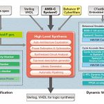
So the design flow is to use profiling to decide what to implement in software and what in FPGA fabric, and then the software to be implemented as software is compiled using a regular C (or C++) compiler, and the software that is to be implemented as hardware is compiled with Vivado HLS (today’s descendent of AutoESL’s AutoPilot). All the interfaces (operating systems, software stubs and links back to the ARM buses) are generated automatically.

Of course, a modern SoC doesn’t just start from thousands of lines of Verilog (or C), it requires IP and to build FPGA-based programmable SoCs requires an IP library and IP integration tools. FPGA design has much smaller teams and often much less skilled so this has to be more straightforward that in the IP assembly world of a modern (non-FPGA) SoC.

Putting it all together leads to a system with everything tied together so that the “inner loops” of the algorithms are implemented using the FPGA fabric and the rest of the system is implemented in software running on the ARM Cortex processor cores.


How well does it work? Well one example: implementing a video encoder such as MPEG that involves motion detection and not retransmitting parts of the picture that are unchanged or merely incrementally moved, can run at full video rate of sixty frames a second which is a speedup of 700 times from just running the algorithm on the ARM processor.

There’s more in the presentation than this. A look at Xilinx’s view of semiconductor technology, educational kits. How about a self driving car? Well, a very small one.

EDPS is in Monterey next Thursday and Friday, April 18th and 19th. The full program is here. Registration is hereand use the promo code SemiWiki-EDPS-JFR to save $50. Call the hotel directly for room reservations.


3D IC: Are We There Yet?

3D IC: Are We There Yet?
by Paul McLellan on 04-13-2013 at 4:42 pm

For the last few years, thru silicon via (TSV) based ICs have been looming in the mist of the future. Just how far ahead are they? Xiliinx famously has a high-end gate-array in production on a 2.5D interposer, Micron has a memory cube, TSMC has done various things in 3D that it calls CoWoS (chip on wafer on substrate), Qualcomm have been working in the area for years, Cadence has talked about several tapeouts. Is it finally going to be real? More than Moore, which used to apply to these types of technologies, going vertical seems to have been somewhat hijacked already to apply to almost anything.

One school of thought is that if you can go the Moore route, going to 20nm or 14nm, then that is the way to go. I’m not even sure about that. At one 3D working group I attended, a guy from eSilicon used their cost model to estimate that Xilinx were saving 80% of the cost by using a 2.5D interposer based approach versus trying to yield such a big die (probably the maximum reticle size) in an immature process.

But once you start to want to mix technologies such as RF and analog, it is difficult to put them on the same wafer and the More route starts to have its attractions. I’ve talked to a few people about analog in the FinFET era and the received wisdom is that you can do some stuff but it is really hard. You have quantized transistor sizes so you can’t always get the ratio you want. But for sure you can put an analog die on an interposer with a FinFET. And you can put DRAM on logic, even lots of DRAM maybe.

There have been some technical issues but the main issue now is whether it is cost-effective compared to other forms of integration.

At EDPS on Thursday Herb Reiter will moderate a session on 3D IC design. The other presenters are:

  • Dusan Petranovic of Mentor, looking at verification
  • Brandon Wang of Cadence, focused on implementation
  • Mike Black from Micron, the strategist behind their memory cube
  • Gene Jacubowski of E-system Design, signal and power simulation

EDPS is in Monterey next Thursday and Friday, April 18th and 19th. The full program is here. Registration is hereand use the promo code SemiWiki-EDPS-JFR to save $50.. Call the hotel directly for room reservations.


TSMC Responds to Samsung!

TSMC Responds to Samsung!
by Daniel Nenni on 04-12-2013 at 10:00 pm

This was the 19[SUP]th[/SUP] annual TSMC Symposium and by far the best I have attended. Finally tired of the misinformation that plagues our industry, TSMC set the record straight with wafer and silicon correlated data. TSMC shipped more than 88 MILLION logic wafers in 2012, more than any other semiconductor company, that gives them significant bragging rights which they rarely exercise. It was standing room only (I counted 1,200+ chairs) not including the 48 ecosystem partner companies manning the booths next door.

The one thing that was not mentioned was the Apple move from Samsung to TSMC starting at 20nm. Considering Apple is responsible for an estimated 70% of Samsung’s foundry business this product shift is devastating. Several ecosystem partners told me that Samsung is cutting budgets for their ecosystem (tools and IP) in preparation for the Apple loss. TSMC on the other hand has 850 people building their ecosystem with an annual shared budget of $1.5B. This ecosystem delivers silicon accurate tools, reference flows, and IP blocks (5k+) for each and every process node. The Chairman (Dr. Morris Chang) calls this, appropriately enough, the Grand Alliance! Interesting notes from the Chairman:

  • Semiconductor industry contracted 2-3% in 2012
  • TSMC customers outperformed the PHLX Semiconductor Sector (SOX)
  • Semiconductor industry to grow 4% in 2013
  • Fabless companies will grow 9% in 2013
  • TSMC will grow “in the teens” again in 2013 (TSMC grew 19% in 2012)

One thing you have to realize about mobile SoCs is that they only have a one year shelf life. The most recent Samsung based Apple A6 SoC will die a very quick death when the TSMC based A7 starts shipping next year. This is a new experience for us as semiconductor professionals. This is changing the way we buy and sell wafers. Don’t get me wrong, price will always be important but the mobile customers also buy technology road maps: What can be delivered when, at what capacity, and at what confidence level. It’s all about setting customer expectations and exceeding them and that was the focus of this symposium.

Dr. Jack Sunreminded us that TSMC is the only foundry to successfully ramp 28nm according to the road maps. 20nm is ramping now three months ahead of schedule and 16FF will start to ramp next year which is half the time it usually takes between nodes. This correlates to what I blogged about before with “Wrights Law” which states that “We learn by doing” or that the cost of a unit decreases as a function of the cumulative production. Other interesting notes:

  • 20nm is ahead of schedule (production starting in 2013)
  • 16nm FF is yielding ahead of plan based on 128MB SRAM test chip data
  • 10nm FF is in process with a 2[SUP]nd[/SUP] generation FinFET (GePMOS)
  • COWOS is in production with multiple tape-outs @ > 95% yield

Dr. Cliff Hou talked about the design challenges from 65nm (low power), 40nm (HKMG), 20nm (double patterning), 16nm (FinFets), and 10nm (multi patterning and spacer). Cliff is a great speaker, very smart, and very personable. If I had to pick the next TSMC CEO it would be Cliff. The most interesting slide he presented for me was the design rule comparisons per node:

  • 700 rules @ 90nm
  • 800 rules @ 65nm
  • 1,200 rues @ 40nm
  • 1,900 rules @ 28nm
  • 3,000 rules @ 20nm
  • 3,400 rules @ 16nm

Now look at the DRC deck size comparisons per node:

  • Just under 20,000 @ 90nm
  • Just over 20,000 @ 65nm
  • Just under 30,000 @ 40nm
  • Just over 40,000 at 28nm
  • Right on 80,000 at 20nm
  • Just under 100,000 @ 16nm

Using this data and a very complex algorithm would put 10nm rules at 5,000 and DRC deck size at 250,000. Are we really prepared for this kind of complexity with our current DRMs in PDF formats?

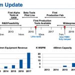
J.K. Wangfollowed Cliff with some very interesting data on building fabs. Paul McLellan did a nice blog on it already: How Long Does it Take to Go From a Muddy Field to Full 28nm Capacity? J.K. is one of the original TSMC employees so you can bet he can build a fab.

If I had to sum up the conference in one sentence here it is:

Semiconductor foundries are presenting very aggressive technology road maps.
The question is: Which one can you trust to deliver?

lang: en_US