For decades we have used a model of faults in chips that assumes that a given signal is stuck-at-0 or stuck-at-1. And when I say decades, I mean it. The D-algorithm was invented at IBM in 1966, the year after Gordon Moore made a now very famous observation about the number of transistors on an integrated circuit. We know that stuck-at faults are not the best model for what can go wrong on an IC but it does work surprisingly well. If you can detect if every signal on a chip is stuck then it turns out you can detect a lot of other stuff that might go wrong (such as two signals bridging together).
But one particular problematic area is detecting transition faults. These are faults that, due to excessive resistance or capacitance, or perhaps one of a number of transistors in parallel being faulty, cause a signal to transition slowly. Slow-to-rise and slow-to-fall faults. If test is not being run at the normal clock rate these might not be detected since at the slower speed the circuit behaves correctly. When these first became a big problem was still in the era when manufacturing test used functional vectors and running them at-speed would automatically pick up these faults. But that approach ran out of steam and today all chips are tested using some sort of scan-test methodology during which the chip is in a special mode and even further from its normal behavior. Scan coverage works on these faults by setting up an initial condition, pulsing the clock twice and then latching the result, or similar approaches that run the transition at speed.
It turns out that most faults are easy to detect but a few hard to detect faults can make a big difference to either the fault coverage or to the time taken by the ATPG (because it has to work very hard to detect the hard to detect faults by definition. Otherwise they wouldn’t be hard to detect duh!). We can make the concept of “hard to detect” more rigorous by the idea of random resistance. No, this isn’t resistance in the resistance-capacitance-inductance sense. It is how likely a fault would be to get detected by a set of random vectors. If almost any set of random vectors will detect the fault it is easy to detect; if very few (or even none) random sequences detect it then it is hard to detect. A design (or a block) is random resistant if random vectors do not automatically have high fault coverage due to there being too many hard to detect faults.
ATPG is done late in the design cycle so we don’t want to discover test problems then, when it is very expensive to do anything about it (changing the RTL after place & route, known as ECO, is orders of magnitude more time consuming than fixing the RTL before starting physical design). What we would really like is a tool at the RTL level that will tell us if we are creating hard to detect faults. We can change the RTL to remove them. Atrenta SpyGlass DFT DSM (SDSM from now on, that is too much of a mouthful) product is such a tool.
SDSM gives feedback on 4 aspects of design at RTL:
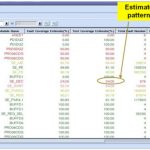
- distribution of nodes (in sorted order) with probable control to 0
- distribution of nodes with probable control to 1
- distribution of nodes with probability of observe
- distribution of nodes with probability of detect
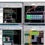
This allows the designer to quickly zoom into blocks where the coverage is low. SDSM can then display a sort of thermal map showing where the hard to detect faults are hiding. Typically in places that have very wide logic cones (forcing ATPG to generate a huge number of vectors to cover all possibilities) or similar issues that are not usually hard to change once identified or can simply be fixed by adding additional test points.
SDSM can identify both scannability and low fault coverage issues early and help designers fix problems without requiring iterations during the implementation flow.
Atrenta’s new white paper on Analysis of Random Resistive Faults and ATPG Effectiveness at RTL is here.
If you are attending ITC in Anaheim, Atrenta is at booth 306.