RVN! 26 Banner revised (800 x 100 px) (600 x 100 px)

So Easy To Learn VIP Integration into UVM Environment

So Easy To Learn VIP Integration into UVM Environment
by Pawan Fangaria on 07-02-2014 at 7:30 am

It goes without saying that VIPs really play a Very Important Part in SoC verification today. It has created a significant semiconductor market segment in the fabless world of SoC and IP design & verification. In order to meet the aggressive time-to-market for IPs and SoCs, it’s imperative that readymade VIPs which are proven with latest specifications must be used to accelerate the complex task of verifying SoCs. And that can happen when there are easy methods available for integrating VIPs into the SoC testbenches and testing them.

It was a pleasant surprise to see this videofrom Cadencewhich demonstrates the integration of PCI Express VIP in UVM Environment with such clarity in just about five minutes. I didn’t think it was so easy to learn. Since Cadence acquired Denali, it has always been ahead in keeping up with the latest specs for PCIe VIP, providing the broadest range of PCIe VIPs covering most of the applications including mobile and cloud, very advanced compliance testing and superb debugging environment. No wonder Cadence is continually advancing in this area of business. The maturity of Cadence’s experience in VIP business is reflected by the kind of seamless integration environment it provides.

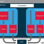
In the UVM environment, multiple agents are put together to stimulate the design, collect coverage and perform self-checking, thus enabling verification of multi-layer components such as PCIe VIP.

The PCIe VIP is integrated into the UVM test environment as UVM agent; multiple agents are encapsulated under the UVM environment. There are active and passive end points to stimulate and monitor the behaviour of the design.

Cadence provides PCIe UVM agent with the installation which can be used straightaway to start verification or it can be customized as per user requirement. The basic verification components such as sequencer, driver and monitor can be extended from the UVM agent. Let’s look at some glimpses of the code which is used to set properties, configure the verification components, and create and instantiate verification components and so on.

On the left side, there is code to set properties for the activeRC component. On the right, there is code for configuring the verification component by extending cdnPcieUvmConfigFunction which is extended from UVM config object. It contains all the functions and attributes of verification. The VIP checks the consistency of all these functions and attributes before starting the verification. The configuration can also be done with graphical interface which allows setting all functions and attributes and checking their consistency.

Above is the code for instantiating and creating verification components. On the left, there is code for instantiating a verification component and virtual sequencer. On the right, the verification component and the virtual sequencer has been created. And a connection between the virtual sequencer and the sequencer of the UVM agent is also created.

Above is the simulation result which can provide very detailed analysis for easy debugging.

This morning, while writing this article, there was another pleasant moment to see Eric Steve’s articleon semiwiki which says about the release of PCI Express 4.0 specifications and its complex features which are already included in Cadence PCIe VIP.

It’s a worthwhile 5 minutes video(presented in a very candid manner by Amir Attarhaof Cadence) to look at and learn how a VIP can boost the productivity of a verification engineer, simplify protocol compliance and shorten the design cycle to meet the short window of opportunity. It’s a must watch for design and verification engineers, students raring to get into semiconductor SoC and IP specialization and others in the semiconductor community.

More Articles by Pawan Fangaria…..

lang: en_US


Is this thing real? Symmetric authentication will tell you!

Is this thing real? Symmetric authentication will tell you!
by Bill Boldt on 07-01-2014 at 6:00 pm

The act of authentication is very straightforward. Essentially, it is making sure that something is real.

There are two parts to authentication:

[LIST=1]

  • Identification
  • Confirmation of identity

    Authentication in the “crypto-verse” typically happens on a host and client basis where the host wants to ensure that a client is real. A typical use case occurs when a client device is inserted into a system, while the host asks (“challenges”) the client to confirm its identity. This can occur when an ink cartridge is inserted into a printer, or a water filter is put into a refrigerator. a battery is put into a phone, and numerous other applications. Firmware and software can be authenticated too, but that is a topic for another article.

    Think of the challenge as when the castle guard in an old movie asks, :Halt! Who goes there?”. The guard expects a suitable response to prove confirm the identity of the approacher.

    Getting back to the real world, authentication is accomplished using a process focused on calculations involving cryptography keys, and that is true for both of the major types of authentication; namely, symmetric and asymmetric. We will focus on the symmetric process here.

    With symmetric authentication, the host and client both have the exact same key, which is in fact how symmetric got its name. Note that is critical for both keys to be kept secret to ensure security. Keeping secret keys secret is the main touchstone of authentication and data security of any type. The best way to do that is using a secure hardware key storage device.

    The basic idea behind symmetric authentication is that if the client is real then it will have the exact same key as the host. Challenge-response is a prescribed methodology to prove it.

    The host controller sends the client a numerical challenge to be used in a calculation to create a response, which is then compared to a similar calculation that is performed on the host.

    To describe the process in more detail we can look at a typical symmetric authentication architecture using Atmel ATSHA204A devices on both the host and client and a microcontroller in the host. (Another article will explain how this is done with the crypto device on the client only, which is the fixed challenge methodology).

    Step 1: The process kicks off when the host sends a random number to the client which is generated by the host’s ATSHA204’s random number generator. This is the “Challenge” and is illustrated above.

    Step 2: The client receives the random number challenge and runs it through a hash algorithm (i.e.SHA256) using the secret key stored there. The result of the hashing function is called the“Response” and it can also be called the “Message Authentication Code” (or MAC). A MAC is technically defined as the result of a hashing function involving a key and message. The response is sent to the host.

    Step 3: The host internally uses the same challenge (i.e. the random number) that it sent to the client as an input to its internal hash algorithm. The other input to the internal hash is the secret key stored on the host side. Then the host compares the hash value (MAC) calculated on the host side with the response hash-value (MAC) sent from client. If the two hash values (MACs) match – then the keys are indeed the same and the client is proven to be real.

    Note that the secret keys are never sent outside the devices, as they always remain securely stored in protected hardware and invisible from attackers. Stated very simply:“You can’t attack what you can’t see.”

    Benefits:
    The benefits of a symmetric architecture with secure key storage crypto engine devices on both sides are:

    • Symmetric authentication with crypto devices on both sides is quite fast.
    • Secure hardware storage on both sides increases security.
    • Ensures a very low processing burden on the microcontroller.

    For more details on Atmel CryptoAuthentication™ products, please view the links above or the introduction page at CryptoAuthentication.

    Bill Boldt, Sr. Marketing Manager, Crypto Products Atmel Corporation


  • A song of optimization and reuse

    A song of optimization and reuse
    by Don Dingee on 07-01-2014 at 10:00 am

    If you hang around engineers for any time at all, the word optimization is bound to come up. The very definition of engineer is to contrive or devise a solution. With that anointing, most engineers are beholden to the idea that their job is creating, synthesizing, and perfecting a solution specifically for the needs of a unique situation. Continue reading “A song of optimization and reuse”


    PCI Express 4 specification just released for PCI-SIG DevCon

    PCI Express 4 specification just released for PCI-SIG DevCon
    by Eric Esteve on 07-01-2014 at 4:45 am

    I have been alerted by a blog from Moshik Rubin from Cadence: PCI-SIG has finally released the PCIe 4.0 rev 0.3 specification for members’ review, on time for the PCI-SIG developers conference last June in Santa Clara. Since the early days of PCI Express in 2005, Denali (at that time, now Cadence) has positioned the PCIe VIP as the first to be released. This aggressive positioning was a part of Denali’s success: being the first on the market greatly helps catching the first PO from customers, large IDM or smaller IP vendors. Getting fresh cash in advance helped minimizing cash investment and boost engineering and product development effort. Sounds like a winning strategy!

    If you take a look at the PCI-SIG website, you can download the conference agenda and realize that PCIe 4.0 is more than a buzz word, as several presentations were specifically dedicated to PCIe 4.0 Electrical, Card Electromechanical Specification (CEM) or Encoding and PHY Logical. You may be surprised by the number of presentations dedicated to M-PCIe, the joint specification issued by the MIPI Alliance and PCI-SIG. In fact, PCIe 4.0 is the first specification fully integrating M-PCIe (M-PCIe was an ECN of PCIe 3.0 specification). Mobile Express attractiveness is still strong within the SC industry, and the M-PCIe dedicated presentation cover an overview, MIPI M-PHY Technical Overview, Testing and Verification of M-PCIe devices and also a Holistic Approach for M-PCIe implementation!


    The Cadence M-PCIe Subsystem IP supports up to height M-PHY lanes in each direction, and has over 100 configuration features and 1500+ input parameters, to customize the subsystem to the specific needs of the application. This very wide configurability capability is directly linked with the PCI Express specification, offering an extensive set of parameters. That is, the Cadence M-PCIe Subsystem IP uses the company’s Silicon proven PCIe Controller core, and the M-PHY Physical layer.

    The logical physical layer provides an RMMI interface to connect the M-PHY device, and the Host Adaptation Layer (HAL), or optional AXI3, provides connectivity to the client. The picture below illustrates the RMMI implementation:

    As usual, Gen-4 specification is doubling the bandwidth while keeping backward compatibility. Let’s review the main changes/additions of the new specification:

    • Speed negotiation and operation at 16.0 GT/s
    • Link equalization procedure for 16.0 GT/s
    • Inferring electrical idle conditions at 16.0 GT/s
    • Reorganization of the PCI Express electrical specification
    • Incorporation of all post Gen3 ECNs (including M-PCIe)

    Cadence PCIe 4.0 VIP was announcedin May and provides support for all of those changes. This VIP has been demonstrated during PCI-SIG DevCon 9 at the Santa Clara Convention Center. As mentioned earlier in this paper, Cadence has adopted the same aggressive Verification IP launch strategy for than Denali. More than just a successful marketing strategy, this policy makes Cadence as essential part of the PCI Express Ecosystem, as IP vendors and IDM need to benefit from a VIP available in advance, before the final PCIe 4.0 specification is frozen, to be able to launch PCIe 4.0 products with a TTM advantage! As far as I am concerned, I also expect to see the PCIe 4.0 Design IP to be released soon by Cadence, as the Design IP group should benefit from the efforts made by the Verification IP team!

    From Eric Esteve from IPNEST

    More Articles by Eric Esteve…..

    lang: en_US


    RTL Signoff Update from #51DAC

    RTL Signoff Update from #51DAC
    by Daniel Payne on 06-30-2014 at 7:00 pm

    In the early days of Customer Owned Tooling (COT) the signoff was done at the GDS II, or physical level. Today, however we see the trend of RTL signoff instead because of the EDA tools and methodology available. At DACearlier this month I met with Piyush Sanchetiof Atrenta to get an update on what’s new with RTL signoff.


    Continue reading “RTL Signoff Update from #51DAC”


    Synopsys Revamps Formal at #51DAC

    Synopsys Revamps Formal at #51DAC
    by Paul McLellan on 06-30-2014 at 6:02 pm

    Synopsys announced verification compiler a couple of months ago and dropped hints about their static and formal verification. They haven’t announced anything much for a couple of years and it turns out that the reason was that they decided that the technology that they had, some internally developed and some acquired, wasn’t a good basis for going forward and they needed to rebuild everything from the ground up. Compared to when their technology was developed, there was advanced power management, hundreds instead of a few clocks, complex protocols and complex interconnect. At DAC earlier this month they announced their new products.

    They use the front end of VCS so that anything that can be loaded into VCS can be loaded into their static and formal tools. That is not to say that their formal tools, in particular, can prove a whole SoC correct, that is just unlikely to ever happen. But they can check, for example, all the connectivity or the clock-domain-crossing (CDC) signals on a whole chip, taking all the reconvergence into account.

    The performance is way up on prior performance. 4X improvement in low power checks, 60X up on formal checks and 180X on sequential checks. That’s a lot.

    On low power static checking they have UPF checks, architectural checks, functional and structural checks and power-ground checks. They support all the latest low power design techniques and have a very close alignment with the implementation flows. One of the big issues with static checking is that one error can cascade lots more and so there is a high noise-to-signal ratio. A hundred errors lead to 20,000 violations and it is hard to find the real errors that need to be fixed.


    The CDC checking works at the full-chip level so can find deep reconvergence bugs. It uses the same setup scripts as DC which makes adoption straightforward. It recognizes all sorts of synchronizer implementations on clock boundaries: extra FF, FIFOs, mux, handshakes and more.

    On the formal side they have rebuilt formal engines from scratch for the toughest challenges. Formal is a weird technology, if one approach can prove something then it doesn’t matter that others cannot. So different engines under the hood can make the whole tool more powerful. And smart users know that if one formal tool can prove something it doesn’t matter that another cannot and so they often use several tools in parallel. The formal tools produce a waveform when they find an issue (a waveform that causes the assertion to fail) and this is fully integrated with the Verdi debug that Synopsys acquired with SpringSoft, making tracking down and fixing the root-cause a lot easier.


    So new technology, several times faster, much higher capacity and easier to use. And all tied into the standard interface of verification compiler.


    More articles by Paul McLellan…


    Virtual Prototype Update from #51DAC

    Virtual Prototype Update from #51DAC
    by Daniel Payne on 06-30-2014 at 12:07 pm

    EDA industry pundit Gary Smithhas been talking about the electronics industry adopting an ESL tool flow for decades, so it was my pleasure to speak with Bill Neifertof Carbon Design Systemsat DAC this month because his company has been offering both tools and models that enable a virtual prototyping design flow.

    Continue reading “Virtual Prototype Update from #51DAC”


    The Intel Resurgence?

    The Intel Resurgence?
    by Daniel Nenni on 06-30-2014 at 8:00 am

    There is an interesting article on Seeking Alpha about Intel. Interesting because it is written by someone with both fabless semiconductor experience and a talent for strategic thinking. It’s a good read and like most Seeking Aplha semiconductor articles the comments are hilarious. Give the guy a penny and click over HERE, he deserves it:

    Little understood by analysts or investors is the fact that Intel has always operated as a one-product company that spins out dozens of derivatives. Desktop, mobile and server chips originate from one common core. This leads to ramping of millions of units quickly and this is key: at incredibly high yields. Every time the company tries to implement a new core and split the markets, it fails. This occurs often and it is why Atom is not the future. Broadwell is well designed to continue the one core processor for all markets and selling from $30 to $6000 depending on number of cores, cache sizes, performance and power.

    Full disclosure: I know the author (Ed McKernan), he started his writing career on SemiWiki and we happen to agree on most things semiconductor with the exception of Apple using Intel as a foundry. It’s not gonna happen Ed!

    I too believe Intel will exit the Atom based SoC chip business. There is serious competition inside Intel between the microprocessor and mobile group and at some point in time there will no longer be room for both, my opinion. I’m told about 10,000 employees are involved with the Intel mobile effort so this would be a serious RIF. It would also be a serious piece of humble pie but I think Intel CEO BK is the right guy to eat it and be stronger as a result. Let’s see what Q2 2014 earnings bring for Intel mobile, my guess is it will be yet another billion dollar loss.

    The funniest comment thus far is an attack on me of course:

    Dan,
    Let’s keep in mind what you consider to be an expert opinion.

    Back in mid-2011 you predicted Intel’s 22nm FinFET was a billion dollar mistake, and you claimed TSMC’s 3D IC technology was already in production yet it hasn’t been seen in public for 3 years now, unless by production you mean the production of powerpoint slides.
    http://bit.ly/TG5xN9.

    About six months after SemiWiki went online I wrote an article about the difference between a 3D transistor (FinFET) and 3D IC (packaging). This guy still does not get it. At that time SemiWiki had about 15k users (viewers) and close to 20k people read the article so that was a big deal. Three years later we have more than a million users and articles about Intel and TSMC still draw the most attention which is why I write them. I also learn as I write, which is the real motivation behind blogging, industry knowledge. Unfortunately sometimes it’s painful to look back at what I’ve posted and this is one of those times.

    This is what I wrote:

    In May of this year Intel announced Tri-Gate (FinFET) 3D transistor technology at 22nm for the Ivy Bridge processor citing significant speed gains over traditional planar transistor technology. Intel also claims the Tri-Gate transistors are so impressively efficient at low voltages they will make the Atom processor much more competitive against ARM in the low power mobile internet market.

    Okay, so far so good.

    Time will tell but I think this could be another one of Intel’s billion dollar mistakes. A “significant” speed-up for Ivy Bridge I will give them, but a low power competitive Atom? I don’t think so.

    The BayTrail 22nm SoC was in fact a billion dollar contra revenue failure but I have no idea what I was thinking when I wrote this:

    Intel already owns the traditional PC market so trading the speed-up of 3D transistor technology for lower power planar transistors is a mistake.

    Say what? :confused:

    More Articles by Daniel Nenni…..

    lang: en_US


    What can you do when your fab closes down?

    What can you do when your fab closes down?
    by Daniel Nenni on 06-29-2014 at 4:00 pm

    A recent report from IC Insights described 72 wafer fabs that have closed in the past five years. Eight more plants have gone in 2014, showing the trend is continuing.

    This leaves their customers with a problem: what can they do when the fab shuts down? Some may recognise that their own technology has reached the end of its life and work on generating a replacement while others will place a ‘last time buy’ to stockpile as many chips as they can. However, most will be left with a headache as they go looking for a new supplier.

    Moving any existing circuit from one foundry to another is difficult and it’s much worse when dealing with legacy chips. Detailed databases may be difficult to locate and the original design team is likely to be long gone, leaving little circuit knowledge for the product. Companies may be left with a few files and a pressing need to find a new supply of silicon.

    As process migration specialists, IN2FAB often works with companies who have to find a new foundry. A redesign will be time consuming and too costly when no new functionality is required so a migration based path to a new supplier is very attractive.

    When facing this problem, the chip’s owner should gather as many design files as possible and a GDSII file and a netlist is usually the minimum. A schematic database is preferred although the tools used to create them may be gone so translators can be used to pull them in to a Cadence system to match the new foundry’s PDK. A layout database made with parameterised cells is useful but polygon based layout will suffice.

    Also read: IC Manufacturers Close or Repurpose 72 Wafer Fabs from 2009-2013

    Analog and mixed signal circuits are typically defined by the transistors’ voltage thresholds and matching of the passives. If the ohms per square in the target process are much lower, resistors will have to grow which can lead to spacing problems and a similar match must be made for capacitors. IN2FAB usually conducts a detailed feasibility study to identify similarities and differences between components which is essential when choosing the new foundry and process.

    Delay files for digital circuits may not be to hand which makes regeneration through place and route almost impossible. Instead, the design can be migrated as a custom circuit to exactly match the original and maintain the placement and routing as before. This retains balance and prevents the introduction of new timing offsets. Digital circuits can often move to a smaller node and gate sizes and routing adjusted to meet the new rules without losing the integrity of the original circuit.

    Other elements like bond pads and ESD or difficult components like inductors must also be considered but the key to the migration is to match the design to the new process and use automation to modify the design as needed. While some dedicated engineering input may be needed to address fine details, the automation in our own EDA technology means that the chip can usually be transferred to the new process in weeks.

    Losing a foundry is a problem but it needn’t be a disaster. Migration technology can move circuits to a new process from basic design files or old CAD systems and bring them up to date, giving them a new lease of life. Redesign is expensive and putting designers to work on old products is poor allocation of resources. Migration presents an effective alternative and is usually the fastest way to move circuits to a new foundry.

    Tim Regan
    President and CTO
    IN2FAB Technology


    lang: en_US