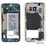
RVN! 26 Banner revised (800 x 100 px) (600 x 100 px)

Physically Aware DFT Improves PPA

Physically Aware DFT Improves PPA
by Pawan Fangaria on 02-16-2015 at 7:00 pm

Introducing on-chip test circuitry has become a necessary criteria for an ASIC’s post manufacture testability. The test circuitry is usually referred as DFT (Design-for-Test) circuit. A typical methodology for introducing DFT circuit in a design is to replace usual flip-flops with special types of flip-flops called ‘scan flip-flops’ that contain logic targeted for improving testability. Scan chains are formed by connecting scan flip-flops serially that allow Automatic Test Pattern Generation (ATPG) tools to control and observe the sequential state of the design and to generate test patterns to achieve the highest fault coverage. Further, extra circuitry can be added to compress test data volume and optimize test time. Also, several self-testing logics, such as logic built-in self-test (LBIST) and memory built-in self-test (MBIST) can be added on a chip.Clearly, the DFT circuits are a must for testability, reliability and robustness of designs. However, they introduce overheads in terms of area and wiring which can increase power consumption and decrease performance of a design substantially. Also, accommodating clock domain crossing (CDC), clock-edge mixing, and voltage domain crossing in an SoC (which can have multiple modes of operations) needs extra hardware such as lock-up latch and voltage level shifter. This extra hardware introduces additional wiring along the scan path resulting into excessive wiring congestion. So, what’s the alternative in such a dilemmatic situation? We truly do not have a choice. We need to use the DFT circuitry. What if we have the best of both worlds? Here is a smart methodology where the overall design is optimized for best PPA (Power, Performance and Area).The idea revolves around doing design placement before test circuit insertion. Traditionally, placement is the last stage in the design flow when scan chain re-ordering is done to shorten long wires in the scan-paths. Naturally, this approach is limited in the sense that placement cannot be changed to a large extent. The break-point logic on the scan-path that involves lock-up latches, clock crossings, etc. cannot be affected to re-order flip-flops. Hence only feasible long wires can be re-routed. In a new approach at Cadence, a scan-mapped netlist is placed just after synthesis, before inserting DFT. Then, based on the placement, scan flip-flops are assigned to scan chains. Further, scan chain re-ordering is done as a final step.Cadence implemented this new methodology on a real wireless communication chip by using its ‘Encounter Digital Implementation System’ and ‘Encounter RTL Compiler Advanced Physical’ that provided an impressive gain of ~16% in scan-chain wire length reduction compared to traditional methodology. The net result in PPA optimization was ~42% saving in total negative slack in timing, ~5% saving in power and ~2% saving in area. Actual detailed data and the detailed steps applied in the flow by using these tools can be found in a whitepaperfreely available at Cadence website.The whitepaper also describes about how Encounter RTL Compiler leverages I/O pad placement information to optimally order the boundary-scan cells in the boundary-scan shift register. IEEE 1149.1 boundary-scan testing is essential for board-level interconnect testing. Here, boundary-scan cells are inserted between I/O pads and the system logic. The boundary-scan cells are serially connected and provide controllability and observability to board-level interconnects. Their ordering is also important to minimize long crossovers along functional paths.The Cadence’s physically aware DFT methodology is proven to prevent wiring congestion due to DFT insertions, thus providing significant improvements in power, performance and area optimizations of a design.


Secure Processor for IoT

Secure Processor for IoT
by barun on 02-16-2015 at 1:00 pm

In my last blog “Processor for IoT” I have discussed security as one of the key requirements for processor used in IoT devices. In this blog we will analyze different method of hacking and some techniques which can be used to prevent those security breaches.

One of the common ways of attack is to probe address and data bus between processor and memory/ IO devices. The attacker can monitor or override information on those buses. The easiest method of preventing such attack is to encrypt any information (data or address) going out of processor and decrypt them before use inside the processor. This can ensure the confidentiality of the information. To ensure integrity of the information, i.e. the data is not corrupted by an external source; one can add a signature using encryption methodology on the block before sending out of the processor to the memory. When the data is again retrieved from memory the same operation is performed and both the signatures are compared to ensure data integrity. Both encryption and authentication can be performed together by a range of algorithms, commonly referred to as, authenticated encryption.

Now the issue is both the techniques is extra latency delay generated by the encryption and decryption mechanism as well as additional area overhead needed. Particularly the latency may become a critical issue if processor’s response time is required to be low like in real time application environment. One of the remedy deployed is to have dedicated crypto processor where the encryption and decryption are implemented in hardware leaving the main processor free for regular computation.

The next question on security arises where to store the key which is used for encryption and decryption. The key should be protected from outside attacks; otherwise the encryption and decryption will have no impact. Typically the key used to be stored in an on chip non volatile memory. But it may include the cost of manufacturing as it may need some special fabrication process (like EEPROM).

But these processes are not fully secured from physical attacks where the hacker has physical access of the chip and can extract the secure information by timing analysis, power analysis. Usage of physically un-clonable function (PUF) is a solution of this solution. In PUF the key is generated from the physical characteristics of a particular chip (for example delay of a particular circuit in a chip). Even if the hacker knows the circuit used to generate the key he cannot reproduce the same delay due to the variations of manufacturing process. Also this does not need any extra manufacturing process.

Another techniques used by designer to prevent timing attack is to introduce random delay to prevent attacker know the timing of its desired operation from reset of the system. To make it more effective the time period of the clock itself is randomized in low frequency application like smartcard. Designer can also impose randomness in the power consumption, electromagnetic radiation to prevent power analysis and electromagnetic analysis attacks respectively.

Trojan is another new way which new generation hackers are using to change the functionality of a circuit from its normal mode and make the circuit behave as per hacker’s need to extract confidential information from the circuit. Trojans are small module which is put by a hacker who has access to design files of an SoC or it may comes from a third party module which is reused inside an SoC. Trojans are typically dormant and hence make it difficult to get identified in the circuit. But in some rare event, Trojan gets activated. To prevent this circuit designer put a small monitoring block which monitors the functionality of different portion of the circuit and flags an error whenever any abnormality in circuit functionality is observed.

Barun Kumar De, Senior Business Development Manager – SmartPlay Technologies


ARM 2014 Results: 12 Billion Cores

ARM 2014 Results: 12 Billion Cores
by Paul McLellan on 02-16-2015 at 7:00 am

Last week was the ARM earnings call, giving the Q4 results and a summary of 2014. 12B chips containing ARM processors were shipped last year which has meant that they have grown in all their major end-markets: mobile, embedded intelligence, and enterprise infrastructure. Almost half of those 12B chips were in mobile, around 5.6B. That is obviously a lot more than the total number of smarphones shipped (1.3B) meaning that there are, on average, four to five ARM processors in each smartphone. Of course the one in the application processor gets all the attention and is probably the only one that is a high-end 64-bit Cortex-Ax core.


If you want some evidence that IoT is really a thing and is not just pure hype, then ARM has some numbers:around 200 companies in total with Cortex-M and what are, many of those companies are doing is generating products for these new emerging markets wearables, smart devices, IOT, which integrates a different technologies in different ways to address new and growing markets

Their market share in networking has doubled year on year from 5% market share to 10%. This is all still 32-bit since this is not an industry with short design cycles. So there is future upside with the V8 instruction set to address a bigger market (and carries higher royalty rates).

ARM reckons they are now the #1 GPU vendor with their Mali series with their partners shipping 550M chips. I’m guessing that means they believe they have overtaken Imagination who are the only other serious GPU IP licensor, most notably to Apple for the iPhone.


One statistic they reported, which they never have before, is how many chips contain ARM’s physical IP (descendants of the old Artisan product line). The answer is 8.9B. I don’t know if that is only chips that contain ARM processors, obviously you can use ARM standard cells without having a processor on your chip. That is 2/3 of the number of chips shipped with ARM cores anyway.

Last year ARM teased analysts by pre-announcing a product with a code-name Maya. This turned out to be the Cortex-A72 announced a couple of weeks ago along with a suite of other products. On the call they started teasing again, pre-announcing two new products called Teal and Grebe, although they gave not a hint as to what sort of products these might be.

See also New Suite of ARM IP for Mobile

One surprising statistic is that they expect that by the end of this year around 50% of the cores shipping will be 64-bit, including more than 30% of mobile devices.

ARM was asked about how much share they anticipated Intel getting in mobile with their agreements with Rockchip and Spreadtrum. Simon wasn’t going to go there that directly but they are clearly not quaking in their boots:So we’re not assuming any significant market share loss in smarpthone in any of the numbers and outlook that we’ve given today. I think we’ve got an excellent portfolio of technology that’s got enable ARM and our licensees to continue to succeed in that space. So we’re not baking in some big share loss and therefore there is not the opportunity that doesn’t materialize. I think over the foreseeable future here, over the lifetime of the products that we have, our shares there are looking good.


So great results. To me the most surprising number was the explosive growth of 64-bit when you think that it was only introduced a year or two ago and ARM expects to exit the year with over half of their partners’ shipments being 64-bit. Given that they also expect a lot of growth in the IoT/Cortex-M end of the business, which is all 32-bit, this is impressive. They also said that they expect to have 20% of the server business by 2020, which would be an amazing achievement if it turns out that way.

Next place to get your ARM fix: it is Mobile World Congress in Barcelona in a couple of weeks. Expect to see lots of ARM v8 smartphones announced.

Transcript of call here. Slides here.


Greetings from Digitopia!

Greetings from Digitopia!
by Bill Boldt on 02-15-2015 at 7:00 pm

digitopia

When it comes to the privacy and security of data, what does the future hold for consumers, companies and governments?

A tremendously interesting document, called “Alternate Worlds,” was published by the U.S. National Intelligence Council. It’s a serious document that not only examines four different alternatives of what 2030 might look like, but possesses some major geo-political thinking about the future.

In the entire report there was only one comment regarding privacy, which is amazing. This brings up many questions. Has privacy already become a quaint notion and a relic of times past? Is the loss of privacy a done deal? Will there be any attempt at reclaiming personal privacy? Will renewed privacy only be available to the upper classes? Will companies be required to take responsibility for embedding more security and privacy in their products and systems? Will governments fight for citizens’ rights to privacy or insist on the right to intrude? These all are important 21[SUP]st[/SUP] century questions, and they are simply impossible to answer now given that there are far too many variables. Only time will tell.

At the moment, however, it is pretty clear that the trend is away from privacy, at least in the way that privacy was defined in prior generations. If you observe first-world high school and college kids, you can easily see that many, if not most, live their lives way out in the open on apps like Facebook, Twitter, Tumblr and others, and don’t really seem to care all that much who is watching. Lately, more limited audience apps like WhatsApp, Snapchat, and WeChat that focus on smaller groups rather than general broadcasts have been growing, which belies some return to privacy concerns (i.e. don’t let mom see this), but the generational theme is clearly “live out loud.” Younger people live in a type of virtual society. Let’s call it “Digitopia.” Digitopia is far from a utopian place because it is insecure — really insecure. Cyber criminals, nosey companies, sneaky governmental operators, and other techno-mischief makers run rampant there.

One of the more intriguing predictions in the Alternate Worlds report points to future brain-machine interfaces that could provide super-human abilities, as well as improve strength, speed and other enhancements (i.e. bestow super powers). This notion could have come right out of author William Gibson’s classic cyber-punk novel Neuromancer where people’s brains directly “jack-into” the matrix. The report states:

“Future retinal eye implants could enable night vision, and neuro-enhancements could provide superior memory recall or speed of thought. Neuro-pharmaceuticals will allow people to maintain concentration for longer periods of time or enhance their learning abilities. Augmented reality systems can provide enhanced experiences of real-world situations. Combined with advances in robotics, avatars could provide feedback in the form of sensors providing touch and smell as well as aural and visual information to the operator.”


Hanging Out in Digitopia

Even the peaceful denizens of Digitopia are by default reckless, especially when it comes to their own privacy.

“A significant uncertainty … involves the complex tradeoffs that users must make between privacy and utility. Thus far, users seem to have voted overwhelmingly in favor of utility over privacy,” the Alternate Worlds report states.

As introduced in a prior article calledDigital Annoymity: The Ultimate Luxury Item,”the desire for personalized services is very seductive, and consumers are now complicit in, and habituated to, revealing a great deal about themselves. Volunteering information is one thing, but much of the content about our digital selves is being collected automatically and used for things we don’t have any idea about. People are increasingly buying products that automatically track their lives including cars storing data about driving habits and downloading that to other parties without the need for consent. As we visit web pages, companies get access to our digital histories and bid against each other in milliseconds fir the ability to display their advertising to us. This is kind of creepy. There is now an unholy trinity of governments snooping on us, corporations targeting our buying behaviors, and cyber-criminals trying to rip us off. The antidote is better security, but cyber-security is not something that individuals will be able to make happen on their own.

Data collection systems are not accessible, and they are not modifiable by people without PhDs in computer science. Because of that, security and privacy could easily become commodities which consumers will demand and thus economically force companies to provide. The only weapon consumers have is what they consume. If consumers only purchase secure products, then only secure products will succeed. In Digitopia, a company’s success may become dependent simply upon how well they protect the interests of their customers and partners — that is not a hard concept to understand.

You can almost see how there could easily be the equivalent of a “UL” label for privacy. Products and services could be vetted for the strength of their security mechanisms. Subsequently, products should then be rated on if they have encryption, data integrity checks, authentication, hardware key storage, and other cryptographic bases.

Beyond the testing of the products themselves, there could easily be businesses set up to provide secure protections to individuals and companies like a digital Pinkerton’s for digital assets. It is likely that those who can afford digital anonymity will be the first to take measures to regain it. To paraphrase a concept from a famous American financial radio show host, privacy could replace the BMW as the modern status symbol. The top income earners who want to protect themselves and their companies will be looking for a type of “digital Switzerland.”

Regaining privacy will likely democratize over time as the general population will demand the same protections as the 1%-ers. Edward Snowdon showed us that everyone is under some sort of surveillance, so we have to face the facts that data gathering on a grand scale is part of the world now and will only grow in scope. However, we don’t have to just accept insecurity because things can be done, including adding secure devices to digital systems.

The Future Belongs to the Middle Classes

Maybe the most important factor noted in the Alternative World report has to do with the forthcoming growth of middle classes. As populations increase and more people worldwide move into the middle class, a growing number of people and things will be connected. That is why the Internet of Things is expected to grow so quickly. More connected things means more points of attack, and more data gathering for legitimate and illegitimate purposes. Therefore, the need for digital security is tied directly to the number of communicating nodes, which is tied directly to the growth of the middle class. More people with financial means means there will be more things to secure. This is becoming obvious. The middle class buys the lions’ share of products and services, and more of those products and services and how they will be ordered and delivered will be electronic. More people, more electronic things, more need for security.

When it comes to population, South and East Asia are the elephants (and dragons) in the room, as the chart below demonstrates.

The most powerful trend going forward is arguably the emergence of new “super-sized” middle classes in China and India. The worldwide middle class will grow exponentially, and it has already started to super-charge demand for food, energy, and manufactured products — particularly smart communicating electronic devices, many with sensing capabilities. That, of course, is how the IoT is getting started. Major companies are holding out the IoT as a way to drive efficiencies in production and distribution while keeping costs low. You can see that in the literature of major companies such as GE who is targeting the Industrial Internet of Things as a major strategic vector.

Population and purchasing power go hand-in-hand, and the evolution of smart, secure, and communicating systems will follow. As Stalin said, quantity has a quality all its own. That is why Asia matters so much.

From the demographic analyses, you can see that most Digitopians will be physically living in South and East Asia and this will continue to rise with time. So, what does that mean for security and privacy?

There is a very different view of the privacy rights in Asia due to a varied tapestry of intricate and ancient cultures — cultures that differ from Western traditions in many ways. However, it must be pointed out that that Western governments are far from the white-knight protectors of privacy rights by any means. Even with uncertainty in how privacy will be embraced (or not) long-term woldwide, in the short- to medium-term, enhanced security will have to filter into networks, systems, and end products, including the IoT nodes. You can look at that as securing the basic wiring and digital plumbing of Digitopia, even if governmental institutions retain the right to snoop.

Practical Security

To close on a practical note, in the short- to medium-term there will be a strong drive to embed more robust security to embedded systems, PCs, networks, and the Internet of Things. Devices to enhance security are already available, namely crypto element integrated circuits with hardware based key storage. Crypto elements are powerful solutions, whose fundamental value is only starting to be recognized. They contain cryptographic engines to efficiently handle crypto functions such as hashing, sign-verify (ECDSA), key agreement (ECDH), authentication (symmetric or asymmetric), encryption/decryption, message authentication coding (MAC), run crypto algorithms (elliptic curve cryptography, AES, SHA), among many others. Together with microprocessors that run encryption algorithms crypto elements easily bring all three pillars of security (confidentiality, data integrity, and authentication) into play for any digital system.

As certain forces move the world towards less privacy and more insecurity, it is good to know that there are real technologies that have the potential to move things back in the other direction. To make a fearless forecast, it seems that going forward companies will increasingly be held liable for security breaches, and that will force them to provide robust security in the products and services that they offer. Consumers will demand security and enforce their preferences with class action legal remedies which they are damaged by lack of security. The invisible hand of the market will point towards more security. On the other hand, governments will argue that they have a duty to provide physical and economic security, which gives them license to snoop. Countervailing forces are in play in Digitopia.

Bill Boldt, Sr. Marketing Manager, Crypto Products Atmel Corporation


AMAT Earnings Call: Next Generation FinFETs?

AMAT Earnings Call: Next Generation FinFETs?
by Paul McLellan on 02-15-2015 at 9:00 am

The Applied Materials earnings call was last week. As usual I”m not all that interested in the financial details of the quarter and I’m certainly not the person to pick whether the stock is going to go up or down in the immediate future. However, there is always interesting information to be gleaned from the semiconductor equipment industry. Facts which are debatable in one part of the industry are just accepted as given in the equipment industry. For example, when Intel cancelled fab 42 in Arizona everyone in the equipment industry had their orders cancelled so they all knew before Intel announced anything.

There are a number of transitions going on right now that are driving Applied’s business. FinFETs in the SoC world and 3D NAND in the memory world and increasingly complex DRAM processes. All of these require additional spending. They reckon that 2014 was up 15% over 2013 and that 2015 will be slightly up again, although with spending biased to the second half of the year. The split last quarter

One interesting question is why foundry is back-end loaded this year. Normally it is front-end loaded to get capacity in place for the heavy consumer volumes in the second half (and Apple typically announces a new model in the fall which requires volume to be in place to build it all). They said that it was due to the FinFET ramp being later than forecast. They explicitly said the July and October quarters would be strong.

Perhaps the most interesting answer to the linearity question was this:One other thing I would say on the foundry business is that this is a huge competitive battle for our customers. So I would expect there’s going to be more technology buys also than we would normally see. There’s certainly the race to the first generation FinFET but there’s also, in parallel, a tremendous pull from customers as they drive to second generation FinFET from a technology perspective. So that’s another thing that we see very strong pull from customers that could play out. And we’re talking about second half of our fiscal year. So it could play out a little bit more in the second half of our fiscal year.

I’m not really sure what this refers to. It is certainly not Intel since they have 14nm in production which is their second generation (Intel’s 22nm was also FinFET although they call it TriGate). I don’t think TSMC’s 16FF and 16FF+ are different enough to require a major equipment investment, they are layout compatible after all (which doesn’t mean that the details of the process are all the same, of course. Something has to be different in the transistors). And it can’t be referring to 10nm since that won’t ramp to volume (when the major equipment buys will take place) before the end of Applied’s financial year in October. If you have good ideas then then be sure to comment below.

It came up again later in the questions:So all of these companies are extremely focused. They’re investing a lot also in technology so they can shorten their cycle between first generation and second generation and all of that is very good to us because, as we’ve said before, our total available market increases a significant amount and we’re very leveraged around the transistor.

At one point they were asked about the difference between first and second generation FinFETs. The answer was not especially illuminating:Well, the FinFET technology is really very heavily weighted, if you look at Epi for instance. The number of Epi steps continue to grow and that’s just a tremendous opportunity for us. NDP steps also are — that’s a great TAM for us and FinFET. We’re also seeing actually a next-generation FinFET technologies, more opportunities in areas like implant. The customers are very focused on trying to drive down the cost of multiple patterning but the number of steps are certainly increasing. We have some technologies we talked about, selective material removal being an area that we see very high growth. And that’s another area that we believe is going to be a big focus for our customers certainly as they go to second generation FinFETs. So our strength is really around the transistor and that’s what FinFET is all about and so that leverages many areas where we have technology leadership.

Another interesting answer was on China. As you probably know, China has a strategic goal to increase the quantity of semiconductor manufactured in China rather than just consuming them. The goal I’ve heard is 40% by 2020. This is especially important in mobile where China is already 3 times the size of the US market, for example, in units. But Applied isn’t seeing it even looking out a couple of years:We don’t really see a significant change in the CapEx spending in China…But in China, we have a very, very good position, very good relationship. So if that spending would ramp, that would be a good thing for us. But we really don’t see a big change there in the next year or 2.


TSMC 20nm Essentially Worthless?

TSMC 20nm Essentially Worthless?
by Daniel Nenni on 02-15-2015 at 7:00 am

It happens at every process node, professional journalists write that something is broken and blames TSMC like a worn out record. To be fair they are not semiconductor professionals with access to the fabless semiconductor rank and file and are easily manipulated which is what happened again at 20nm. Remember when NVIDIA suggested that TSMC 20nm was economically challenged? And the media changed that to “essentially worthless?” Thankfully Apple knew better otherwise we would not have the amazing iProducts we have in our hands today.

Nvidia deeply unhappy with TSMC, claims 20nm essentially worthless
By Joel Hruska on 3/23/2012

Back at 40nm I was the foundry liaison for an IP company and the GPU part of AMD was a big customer. I was the executive sponsor for AMD meaning that whenever there was an escalated problem it landed on my desk. And there were ALWAYS escalated problems at the bleeding edge of GPU design, absolutely.

As 40nm was ramping NVIDIA came out and said their GPUs would be delayed because of yield problems and they pointed fingers at TSMC. The media jumped all over this of course but the AMD guys and I had a good laugh because AMD did not have the same yield problems. At 40nm they had these things called “recommended design rules” (RDRs) to increase yield. One of them was doubling the vias in case there was a one in a billion failure. Of course this increased area and capacitance so the clever NVIDA designers did not do it and had billions of single vias. AMD on the other hand respected the RDRs and beat NVIDIA to 40nm. When the dust settled NVIDIA did admit to design related yield issues but that was not front page news of course.

The same thing happened at 28nm when the fabless guys talked about wafer shortages on conference calls as an excuse for not making their Wall Street targets. The media immediately played the yield card and threw TSMC under the bus. Come to find out TSMC built 28nm capacity based on customer forecasts which were half of what they should have been. TSMC ended up with 100% market share at 28nm versus the 50% forecast and the rest is history.

Nvidia Blames TSMC’s 28nm Process Technology for Slow Sales
by Anton Shilovon 05/11/2012

In March of 2012 NVIDIA came out saying 20nm was not economically feasible and blamed TSMC. In fact, NVIDIA made a detailed presentation at the International Trade Press Conference. The media was all over it reporting in detail WHAT was said but not once considered WHY it was being said and WHY at that particular venue. The entire fabless semiconductor ecosystem had a good laugh because silicon doesn’t lie like people do and the last laugh would be ours.

Some points to ponder:
[LIST=1]

  • Why was this presented at a press conference versus a technical conference?
  • The NVIDIA CEO and TSMC CEO are very close friends, right?
  • The media says GPUs will skip 20nm for 16nm
  • 16nm is really 20nm with low power FinFETs, right?
  • NVIDIA has a 20nm Tegra SoC in production
  • Apple has two 20nm SoCs in production
  • Oracle has a 20nm high performance CPU in production
  • Xilinx has 20nm FPGAs in production

    So tell me, what really happened to the 20nm GPUs?

    Disclaimer: This is written from my aging memory so correct me if I’m wrong here…


  • Do You Need a Silicon Catalyst?

    Do You Need a Silicon Catalyst?
    by Daniel Nenni on 02-14-2015 at 7:00 pm

    Lately there has been significant concern over the rising costs of designing in silicon and the troubling decline in venture investments in semiconductors. These alarming trends include fewer IPOs, a falloff in the amount and frequency of early stage seed investments, and comparatively low industry organic growth rates. A new company called Silicon Catalyst has recently been formed to address some of the key challenges facing entrepreneurs attempting to innovate in semiconductors … namely the challenge of raising sufficient funding and obtaining the appropriate design, prototyping, and test capabilities to move from concept to working prototypes.

    While there are other incubators for software and some for hardware, Silicon Catalyst looks to be the first focused exclusively on startups creating solutions in silicon. Co-founded by three semiconductor veterans: Mike Noonen, Rick Lazansky and Daniel Armbrust, the incubator announced its initial partners last month. They are industry leaders Synopsys, TSMC and Keysight (formerly Agilent) who will provide design tools, fabrication and test capabilities respectively.

    “The launch of this startup incubator parallels TSMC’s emphasis on a ‘Grand Alliance’ of collaborating companies in the semiconductor industry to increase innovation,” said Rick Cassidy, President, TSMC North America. “TSMC is pleased to join the efforts of Silicon Catalyst to help the next wave of fabless semiconductor start-ups achieve success.”


    “A vibrant start-up community is a valuable component in the development of any business and the multi-trillion-dollar industries that we enable,” commented Aart de Geus, Chairman and co-CEO, Synopsys. “Synopsys is proud to be a Silicon Catalyst founding partner to support semiconductor solution start-ups.”

    The Silicon Catalyst incubator’s initial location in Silicon Valley is expected to be announced shortly. Startups are expected to come from universities, industry entrepreneurs and spinouts not just in Silicon Valley but from all around the world. Silicon Catalyst plans to collaborate with local incubators to enable these entrepreneurs to leverage the Silicon Catalyst partner resources without needing to relocate. The first round of screening is expected to begin within the next two months.

    Silicon Catalyst is engaged in discussions with many industry strategic partners who are expected to help select, guide, invest in and be potential acquirers once the startups graduate from the incubator (over a maximum of 24 months). In addition to some modest funding of up to $500k and providing access to the essential services needed for new designs, Silicon Catalyst intends to pair each startup with an experienced mentor who can provide relevant advice and assistance which is viewed as essential to address the challenges that these early stage companies inevitably encounter.

    Investors are mostly ignoring early stage semiconductor investments, however Silicon Catalyst and its partners believe we are entering a long term wave of innovation that requires new semiconductor innovation at their core to address opportunities in IoT, biotech, energy, transportation and mobile. Inspiration for an improved business incubation model and an accompanying vibrant startup community came from the biotech and pharmaceuticals industries that have found ways to address the high upfront costs of device and drug development. Since upfront costs are significantly reduced, start-ups are expected to become much better investments since funding can go directly to innovation and value creation. Silicon Catalyst expects to see renewed interest over time from angel, strategic, and venture investors as a result.

    It will be interesting to see how the semiconductor industry embraces and supports this new model. Optimistically, with sufficient backing, we will look back on this as an important part of today’s fabless semiconductor ecosystem, absolutely.


    More Test Points are Better

    More Test Points are Better
    by Daniel Payne on 02-14-2015 at 7:00 am

    I got really involved in testability back at CrossCheck in the 1990’s when they designed a way for Gate Arrays to have 100% observability without any Design For Test (DFT) requirements on designers. The Japanese Gate Array companies loved this approach and their customers enjoyed the highest test coverage without being test experts. Fast forward to today and we find much less use of Gate Array technology, while new SoCs can have billions of transistors that need to be tested in a reasonable amount of time. About a decade ago the concept of embedded test compression came into the marketplace, a technique where the number of internal scan chains is increased while shortening their lengths. The test software can then control the contents of each short scan chain to maximize test coverage in the least amount of time. Here’s what the hardware looks like for Embedded Deterministic Test (EDT) compression:

    The benefits of test compression are:

    • Spending less time on the tester, which in turn saves costs
    • Achieving higher fault coverage, weeding out silicon failures so a customer doesn’t receive a faulty part

    Related – It’s a bouncing baby IEEE standard!

    So test compression has been working well and delivering real benefits, but to keep up with growing design sizes something new had to be done to help out. That new thing is adding more test points to a design, a concept that has been around for decades but not really applied to embedded test compression. A test point means that we can control an input, or observe an output somewhere inside our logic.


    Test Points: Controlling an output, and input

    The Automatic Test Pattern Generation (ATPG) software has the challenge of modeling a fault inside our logic and then tracing a path back to the inputs to control the data to stimulate the fault, and then propagating the effects of that fault to an observable output. This new approach is to automatically add test points to make the job of ATPG much easier by running faster and creating shorter patterns, decreasing test costs even more. Here’s the flow of how a test point is analyzed and inserted into a design:


    EDT Test Point analysis and insertion flow

    This particular test flow comes from Mentor Graphics. The analysis and insertion of EDT test points can come either before or after scan insertion. Each inserted test point is selected while minimizing effects to the timing closure process. As a designer or test engineer you do have some control over where test point insertion occurs, if needed.

    Related – What’s next in test compression?

    Some Results

    The idea of EDT test points sounds promising, but what about some actual results? Engineers at Mentor have shared results with this approach on over a dozen different designs showing a reduction in the number of patterns required for covering stuck-at faults:


    Impact of EDT test points on stuck-at fault patterns

    There’s a typical reduction in patterns of about 3.7X, all the way up to 13X best case, so your results will vary depending on the design. For Design A to reach a stuck-at fault coverage of 99.92% required 22,244 test patterns, however when adding just 5K test points the same fault coverage was reached using only 6,373 test patterns for a 3.5X reduction.

    Those are impressive results for stuck-at faults, but let’s consider transition delay faults. Here the average reduction in test patterns is 4X over the 12 designs:


    Transition Delay Faults with EDT test point

    There is a trade off between the number of EDT test points and test coverage so there’s no need to go overboard and add an excessive number of points, because adding more points does increase the gate count and therefore area. A utility provides data so that you can see the number of EDT test points versus pattern count, and make your own design-specific tradeoff.

    A final benefit of using EDT test points is that your ATPG run times get faster by about 3.2x on average:

    Summary

    More test points are better and this test methodology of EDT test points will reduce the amount of ATPG patterns required to achieve a level of fault coverage. You can use this approach with either compressed APTG or regular patterns. The amount of reduced patterns is really design dependent, so why not give it a try? There’s a six page white paper at Mentor for download here that has more details.


    A Comprehensive Automated Assertion Based Verification

    A Comprehensive Automated Assertion Based Verification
    by Pawan Fangaria on 02-13-2015 at 4:00 pm

    Using an assertion is a sure shot method to detect an error at its source, which may be buried deep within a design. It does not depend on a test bench or checker, and can fire automatically as soon as a violation occurs. However, writing assertions manually is very difficult and time consuming. To do so require deep design and coding knowledge, whereas verification engineers neither have such deep coding expertise nor a comprehensive knowledge Continue reading “A Comprehensive Automated Assertion Based Verification”


    TSMC’s OIP: Everything You Need for 16FF+ SoCs

    TSMC’s OIP: Everything You Need for 16FF+ SoCs
    by Paul McLellan on 02-13-2015 at 7:00 am

    Doing a modern SoC design is all about assembling IP and adding a small amount of unique IC design for differentiation (plus, usually, lots of software). If you re designing in a mature process then there is not a lot of difficulty finding IP for almost anything. But if you are designing in a process that has not yet reached high-volume manufacturing (HVM) then there is a new set of challenges. If you are really on the bleeding edge and the volumes are going to justify the cost, then the company has to design its own IP since commercial IP just is not available (think companies like Qualcomm or Apple). For everyone else, they need to wait for a broad portfolio of IP to be available. But they don’t want to wait forever. TSMC has its OIP program to ensure that IP is available as soon as possible, that it is tested in silicon and generally is getting ahead of the curve. After all, TSMC makes money when designs go into production and the critical path for getting a design into production goes right through the middle of having EDA tool flows and IP available.TSMC’s IP ecosystem surpassed the mark of 8,000 registered IPs in 2014, from more than 40 IP partners. TSMC IP Alliance partners, together with TSMC internal IP teams, form the largest and fully qualified IP platform available to IC designers in the world. It is a live ecosystem, constantly evolving to adapt to customer needs. With the new creation of ULP processes targeted to IoT applications, a more comprehensive solution is now necessary. TSMC 3rd party IP vendors will add their expertise, creating updated and new low-power IP for TSMC processes.Last year’s Open Innovation Platform 2014 (OIP) Ecosystem Forum was held in September. Over 1000 customers and partners participated. The main focus was on TSMC’s latest processes, in particular 16FF+. TSMC and its partners made the following announcements:

    • OIP has provided over 12 years of ecosytem enablement
    • a new 28nm 28HPC high performance process offering available
    • 20nm in mass production
    • 16FF+ ready for product design
    • Reference flows for 16FF+ delivered
    • ARM big.LITTLE vaiidated in 16FF+
    • 10FF EDA tools ready for early customer design starts

    At the forum, the TSMC OIP Partner of the Year Awards were announced. First for IP:

    • Foundation IP: ARM
    • Interface IP: Synopsys
    • Analog/Mixed-Signal IP: Analog Bits
    • Embedded Memory IP: eMemory Technology
    • Emerging IP Company: Silicon Creations
    • Specialty IP: Dophin Integration
    • Soft IP: Cadence

    Then the EDA awards for the joint development of the 16FF+ design infrastructure (alphabetical):

    • Apache business unit of ANSYS
    • AtopTech
    • Cadence
    • Mentor
    • Synopsys

    The key to the diagram above is purple is Synopsys, red is Cadence, green is Mentor (I think of blue being Mentor based on their website), yellow is Apache, blue is Atoptech and pink is Invarian.These tools go to create a digital SoC (synthesis, place & route) reference flow that captializes on 16FF+ PPA through optimized tool and standard cell implementation, with a constraint variation model for accurate timing signoff, a self-heating model to address thermal concerns, rush current analysis for powering blocks down and up, and more. They also create a customer reference flow for custom digital and analog/mixed-signal with a complete “number of fins” methodology to replace length/width of planar processes. The flow takes into account layout dependent effects, voltage dependent rule checks and a full transistor-level electromigration (EM) and IR drop analysis flow for power analysis.The release of new ultra-low-power (ULP) processes at mature nodes to support the upcoming IoT opportunities, does not lower the focus of TSMC on wide set of Foundation, Interface and Soft-IP from both TSMC and its IP Alliance partners for the leading edge.