You are currently viewing SemiWiki as a guest which gives you limited access to the site. To view blog comments and experience other SemiWiki features you must be a registered member. Registration is fast, simple, and absolutely free so please, join our community today!
RISC-V conferences have been at full capacity and I expect this one will be well attended as well. Andes is the biggest name in RSIC-V. The most notable thing about RISC-V conferences is the content. Not only is the content deep, it is international from the top companies in the industry. It is hard to find a design win these days without RISC-V content, absolutely.
Nvidia’s Frans Sijstermans (VP of Multimedia Architecture/ ASIC) will present Use of RISC-V in NVIDIA’s Deep-Learning Accelerator.
This one should be a big draw in addition to the keynote from Andes co-founder, Chairman and CEO Frankwell Lin “Celebrating 20 years of driving SIP innovation and 15 years of pioneering RISC-V”.
Here are the other keynotes:
– Charlie Su, President and CTO, Andes Technology – Provides insights on advancing modern computing with Andes RISC-V processor solutions.
– Paul Master, Co-founder and CTO, Cornami – Presenting Fully Homomorphic Encryption, the Holy Grail.
Fireside chat: What’s coming in AI? – Facilitated by Charlie Cheng, Andes, Board Advisor with keynotes from:
– Jeff Bier, Founder, Edge AI and Embedded Vision Alliance
– Pete Warden, Founder & CEO, Useful Sensors
There are two full tracks this year, the main conference track and a developer track. The developer track includes hands-on technical training:
Developer Track – Hands-on Technical Training (Limited Seats!)
Four in-depth, 1-hour sessions designed for engineers who want to dive deep into RISC-V technology. Bring your laptop fully charged!
Optimization with RISC-V Vector ISA – Curious about RISC-V Vectors (RVV) but unsure how it works? This session covers the basics and how it boosts vector performance. You will get hands-on experience writing and running vector software using AndeSight tools on RVV-capable processors.
IAR Professional Tools for RISC-V – Learn how professional tools can help you debug your application more quickly and efficiently, accelerating your time to market. Also, discover how prequalified Functional Safety tools can enhance your products.
Create Your Own RISC-V Custom Instructions – Want to create your own RISC-V Instructions to accelerate your application? This session explores Andes’ Automated Custom Extensions (ACE) for enhancing the RISC-V ISA, with a hands-on demo using Andes Copilot, which automates much of the process.
Unleashing the Power of Heterogeneous Computing: Building a complex SoC with high compute and memory demands? Avoid performance surprises by understanding how CPU and GPU subsystems interact under real workloads and memory hierarchies. This session demonstrates how trace-based simulation can uncover bottlenecks, validate compute and cache architecture decisions, and improve heterogeneous system performance.
I know quite a few of the presenters on the main conference track and I can tell you it is an all star cast. The main conference welcomes all attendees, featuring over ten sessions and speeches that cover the RISC-V market and the development of SoCs using RISC-V across AI, automotive, application processing, communications, and more. Participants will also have opportunities to network with speakers and exhibitors from over twenty sponsoring companies offering IP, software, tools, services, and products.
This really is an excellent networking event at one of my favorite Silicon Valley locations which includes breakfast, lunch and a networking reception.
Event Details:
– Location: DoubleTree by Hilton, San Jose, CA – Time: 8:30 – 6:00 PDT – Admission: RISC-V CON is free to attend – Registration:visit the event website
About Andes Technology
As a Founding Premier member of RISC-V International and a leader in commercial CPU IP, Andes Technology is driving the global adoption of RISC-V. Andes’ extensive RISC-V Processor IP portfolio spans from ultra-efficient 32-bit CPUs to high-performance 64-bit Out-of-Order multiprocessor coherent clusters.
With advanced vector processing, DSP capabilities, the powerful Andes Automated Custom Extension (ACE) framework, end-to-end AI hardware/software stack, ISO 26262 certification with full compliance, and a robust software ecosystem, Andes unlocks the full potential of RISC-V, empowering customers to accelerate innovation across AI, automotive, communications, consumer electronics, data centers, and mobile devices. Over 16 billion Andes-powered SoCs are driving innovations globally. Discover more at www.andestech.com and connect with Andes on LinkedIn, X , and YouTube.
HPC Bandwidth Explosion and 1.6T Ecosystem Interop Need
The exponential growth in data bandwidth requirements driven by HPC systems, AI, and ML applications has set the stage for an ever-increasing need for 1.6Tbps Ethernet. As data centers strive to manage vast data transfers with maximum efficiency, the urgency for interoperability testing intensifies. Developers are compelled to act swiftly as standard development is trying to catch with the industry’s need for speed, conducting interoperability testing with real-world channels, at plug fests, Standard Body Interop testing events, along with early 224G TX and RX compliance characterization with variable channels etc has become a key indicator for real-life deployment. This proactive approach reduces risk and helps ensure that components from multiple vendors integrate seamlessly, maintaining robust and efficient operations.
Samtec and Synopsys Collaborate in Interoperability Testing to Enable 1.6Tbps Systems
Interoperability is the cornerstone of constructing robust systems for high-speed applications. It enables diverse components—such as switches, routers, and interconnects—to communicate and function cohesively without issues. In bandwidth-intensive environments, any downtime or performance degradation can lead to significant operational and financial setbacks. Standardized interoperability facilitates smooth upgrades and integrations, minimizing disruptions and ensuring continuous operation. This level of robustness is achieved through meticulous adherence to interoperability guidelines and rigorous testing.
It is well known that 224Gbps and upcoming 400G will be key for achieving 1.6T and eventually 3.2Tbps data transfers. Samtec and Synopsys continue to push the limits of 224Gbps Ethernet performance, as seen in t, where Synopsys 224G PHY IP and Samtec’s Si-Fly® HD co-packaged and near-chip systems showcased scale-out and scale-up capabilities.
224G Ethernet is the Key for 1.6Tbps Interoperability
The pursuit of 1.6T interoperability is driven by advancements in high-performance 224G SerDes architecture. These SerDes technologies are designed to handle the high data rates necessary for 1.6T Ethernet, enabling long-distance data transmission with minimal power and latency. The robustness and reliability of these architectures are critical for maintaining data integrity and performance in HPC, AI, and ML applications. By leveraging cutting-edge 224G SerDes technology, engineers can ensure that their systems meet the stringent demands of modern data centers.
It’s a really big ecosystem
The 1.6T Ethernet ecosystem is characterized by its diversity, incorporating various connectors, cables, and other components. Each approach offers specific advantages and use cases—LR Direct-attached cable or cabled backplane for longer distances, and NPO connectors for shorter, high-density interconnects. This variety ensures that engineers have access to suitable solutions for a broad range of applications and infrastructure configurations, enabling them to optimize data transmission based on specific operational requirements.
Synopsys and Samtec are at the forefront of driving 1.6T interoperability. Samtec’s next-generation connector solutions are designed to meet the challenges of 224 Gbps PAM4 architectures. Synopsys delivers a best-in-class, widely interoperable 1.6T Ethernet IP solution with silicon-proven and low-power 224G Ethernet. These solutions have undergone extensive third-party interoperability testing, helping ensure that designers can start their 1.6Tbps with confidence today.
Register now for the Synopsys and Samtec webinar to ensure your systems to be low risk and leverage pre-tested, pre-verified, interoperable systems with 1.6T Ethernet IP solutions and advanced interconnect technology.
When people talk about bottlenecks in digital signal processors (DSPs), they usually focus on compute throughput: how many MACs per second, how wide the vector unit is, how fast the clock runs. But ask any embedded AI engineer working on always-on voice, radar, or low-power vision—and they’ll tell you the truth: memory stalls are the silent killer. In today’s edge AI and signal processing workloads, DSPs are expected to handle inference, filtering, and data transformation under increasingly tight power and timing budgets. The compute cores have evolved, but edge computing’s goal is to move the compute engine closer to the memory.
The toolchains have evolved. But memory? Still often too slow. And here’s the twist: it’s not because the memory is bad. It’s because the data doesn’t arrive on time.
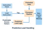
Why DSPs Struggle with Latency
Unlike general-purpose CPUs, most DSPs used in embedded AI rely on non-cacheable memory regions—local buffers, scratchpads, or deterministic tightly coupled memory (TCM). That design choice makes sense: real-time systems can’t afford cache misses or non-deterministic latencies. But that also means every memory access must have exact load latency —or else the pipeline stalls. You can be in the middle of processing a spectrogram, a convolution window, or a beamforming sequence—and suddenly everything halts while the processor waits on data to arrive. Multiply-accumulate units sit idle. Latency compounds. Power is wasted.
Enter Predictive Load Handling
Now imagine if the DSP could recognize the pattern. If it could see that your loop is accessing memory in fixed strides—say, reading every 4th address—and preload that data ahead of time, —commonly referred to as “deep prefetch”—so that when the actual load instruction is issued, the data is already there. No stall. No pipeline bubble. Just smooth execution.
That’s the traditional model of prefetching or stride-based streaming—and while it’s useful and widely used, it’s not what we’re describing here.
A new Predictive Load Handling innovation takes a fundamentally different approach. This is not just a smarter prefetch—it’s a fundamentally different technique. Instead of predicting what address will be accessed next, Predictive Load Handling focuses on how long a memory access is likely to take.
By tracking the latency of past loads—whether from SRAM, bypassed caches, or DRAM—it learns how long memory requests from each region typically take. Instead of issuing loads early, the CPU proceeds normally. The latency prediction is applied on the vector side to schedule the execution at the predicted time, allowing the processor to adapt to memory timing without changing instruction flow. This isn’t speculative or risky. It’s conservative, reliable, and fits perfectly into deterministic DSP pipelines. It’s especially effective when the processor is working with large AI models or temporary buffers stored in DRAM—where latency is relatively consistent but still long. That distinction is critical. We’re not just doing a smarter prefetch—we’re enabling the processor to be latency-aware and timing-adaptive, even in the with or without a traditional cache or stride pattern.
When integrated into a generic DSP pipeline, Predictive Load Handling delivers immediate, measurable performance and power gains. The table shows how it looks in typical AI/DSP scenarios. These numbers reflect expectations in workloads like:
Convolution over image tiles
Sliding FFT windows
AI model inference over quantized inputs
Filtering or decoding over streaming sensor data
Metric
Baseline DSP
With Predictive Load
Result
Memory Access Latency
200 ns
120 ns
40% faster
Data Stall Cycles
800 cycles
500 cycles
38% reduction
Power per Memory Load
0.35 mW
0.25 mW
29% reduction
Minimal Overhead, Maximum Impact
One of the advantages of Predictive Load Handling is how non-intrusive it is. There’s no need for deep reordering logic, cache controllers, or heavyweight speculation. It can be dropped into the dispatch or load decode stages of many DSPs, either as dedicated logic or compiler-assisted prefetch tags. And because it operates deterministically, it’s compatible with functional safety requirements—including ISO 26262—making it ideal for automotive radar, medical diagnostics, and industrial control systems.
Rethinking the AI Data Pipeline
What Predictive Load Handling teaches us is that acceleration isn’t just about the math—it’s about data readiness. As processor speeds continue to outpace memory latency—a gap known as the memory wall—the most efficient architectures won’t just rely on faster cores. They’ll depend on smarter data pathways to deliver information precisely when needed, breaking the bottlenecks that leave powerful CPUs idle. As DSPs increasingly carry the weight of edge AI, we believe Predictive Load Handling will become a defining feature of next-generation signal processing cores.
Because sometimes, it’s not the clock speed—it’s the wait.
Leo Linehan leads Materion’s Electronic Materials business segment, an important supplier to the global semiconductor market and an industry leader in the production of advanced chemicals, microelectronic packaging, precious and non-precious metals, and deposition, reclamation and refining services.
Prior to joining Materion in 2019, he was Vice President and General Manager of Semiconductor Solutions with Element Solutions Inc. and served as Vice President and General Manager of Electronic Chemicals at OM Group. He joined Dow Chemical Company in 2009 as part of its acquisition of Rohm and Haas, where he retained his senior leadership role in Dow’s Electronics Materials business. Earlier in his career, he held several positions of increasing responsibility at IBM.
Tell us about your company.
Materion is a global leader in advanced materials serving a range of industries, including semiconductor, industrial, aerospace & defense, energy and automotive. We’re headquartered just outside of Cleveland, Ohio, and have 3,000 employees around the world. The Electronic Materials (EM) business I lead provides specialty materials for thin film deposition, microelectronic packaging products, and inorganic chemicals. Our business started as a precious metals provider and, through a series of acquisitions, has become a world leader in deposition materials specifically and electronic materials generally.
What problems are you solving?
Our customers are continually seeking a robust, reliable, high-quality supply chain, especially when it comes to new thin film materials for advanced semiconductor production. That’s particularly true given the current geopolitical situation. We hear all the time from customers worried about tariff impacts, sourcing concerns, and volatility in raw materials markets. We’re well positioned to partner with them in mitigating those issues thanks to our international footprint, our broad material portfolio, and the significant investments we’ve made in manufacturing. We have a significant presence in both the U.S. and European markets, with primary manufacturing sites in both regions, which allows us to give our customers valuable insights into navigating these geopolitical realities.
What application areas are your strongest?
When it comes to thin film deposition materials, we serve all segments of the larger semiconductor industry. That includes advanced logic and memory, power semiconductors, and RF semiconductors.
What keeps your customers up at night?
I go back to the idea of having a reliable supply chain. It’s having the right technology that our customers’ customers require when they require it. Our business is fairly evenly split between leading-edge node and mature node semiconductors. There’s still a significant market for semiconductors in mature process nodes, and those processes are still being continuously improved. At the same time, when we acquired HC Starck’s electronic materials business in 2021, that instantly made us a significant player in leading-edge semiconductors as well. There are universal demands that cut across all segments of the semiconductor market related to continuous improvement and supply security. There are also important differences between the advanced process nodes used for logic and memory and the more mature process nodes that are used for power and RF semiconductors that require segment-specific expertise. Ultimately, we work with all of our customers to provide the latest materials that we continuously evolve in order to meet their needs.
What does the competitive landscape look like and how do you differentiate?
The competitive landscape is actually quite complicated. On the leading-edge side of semiconductors, it’s highly concentrated among a relatively few suppliers including Materion. On the mature node side, it’s a diverse landscape with several physical vapor deposition (PVD) sputtering target manufacturers. Many of those are either regional or specialized into very narrow segments. We’re one of the few suppliers that covers the whole landscape, both in terms of semiconductor type and deposition technologies, including materials used for atomic layer deposition. We have a very broad portfolio that encompasses both precious and non-precious metals. That makes us an appealing supply chain partner to a wide range of semiconductor manufacturers.
What new features/technology are you working on?
I already mentioned atomic layer deposition, which is a fast-growing market for us. There is also a constant need for new PVD alloys. For many years, we’ve been known as the company that manufactures PVD targets no one else wants to, and we’re proud of that!
How do customers normally engage with your company?
We mostly sell directly to customers, and we try to engage them in an R&D context when we can. We prefer to have our R&D team engage with their R&D teams, with the sales force facilitating the conversation. We find that’s the best way to solve the critical process issues our customers face all the time.
Whatever software engineering teams are considering around leveraging AI in their development cycles should be of interest to us in hardware engineering. Not in every respect perhaps but there should be significant commonalities. I found a recent paper on the Future of AI-Driven Software Engineering from the University of Aukland, NZ with some intriguing ideas I thought worth sharing. The intent of these authors is to summarize high-level ideas rather than algorithms, though there are abundant references to papers which on a sample review do get into more detail. As this is a fairly long paper, here I just cherry-pick a few concepts that stood out for me.
Upsides
In using LLMs for code generation the authors see increased emphasis on RAG (retrieval augmented generation) for finding code snippets versus direct code synthesis from scratch. They also share an important finding in a blog post from StackOverflow, reporting that blog hits on their website are declining. This is significant since StackOverflow has been a very popular source for exchanging ideas and code snippets. StackOverflow attribute the decline to LLMs like GPT4 both summarizing a response to a user prompt and directly providing code snippets. Such RAG-based systems commonly offer links to retrieved sources but clearly these are not compelling enough to keep up website hits. I find the same experience with Google search, where now search results often start with an AI-generated overview. I often (not always) find this useful, also I often don’t follow the links.
Meanwhile Microsoft reports that the GitHub CoPilot (a Microsoft product) paid customer base is growing 30% quarter on quarter, now at 1.3M developers in 50K organizations. Clearly for software development the ease of generating code through CoPilot has enough appeal to extract money from subscribers.
Backing up a step, before you can write code you need a clear requirements specification. Building such a specification can be a source of many problems, mapping from a client’s mental image of needs to an implementer’s image in natural language, with ambiguities, holes and the common reality of an evolving definition. AI-agents could play a big role here by interactively eliciting requirements, proposing examples and scenarios to help resolve ambiguities and plug holes. Agents can also provide some level of requirements validation, by identifying vague or conflicting requirements.
Maintaining detailed product documentation as development progresses can be a huge burden on developers and that documentation can easily drift out of sync with the implemented reality especially through incremental changes and bug fixes. The authors suggest this tedious task could be better handled through agent-based generation and updates, able to stay in sync with every large or small change. Along similar lines, not everyone in the product hierarchy will want detailed implementation doc. Product managers, AEs, application developers, and clients all need abstracted views best suited to their individual interests. Here also there is opportunity for LLMs to generate such abstractions.
Downsides
The obvious concern with AI generated code or tests is the hallucination problem. While accuracy will no doubt improve with further training, it is unrealistic to expect high certainty responses to every possible prompt. Hallucinations are more a feature than a bug, no matter how extensive the training.
Another problem is over-reliance on AI. As developers depend more on AI-assisted answers to their needs, there is a real concern that their problem-solving and critical thinking skills will decline over time. Without expert human cross checks, how do we ensure that AI-induced errors do not leak through to production? A common response is that the rise of calculators didn’t lead to innumeracy, they simply made us more effective. By implication AI will reach that same level of trust in time. Unfortunately, this is a false equivalence. Modern calculators produce correct answers every time; there is no indication that AI can rise to this level of certainty. If engineers lose the ability to spot errors in AI claims for such cases, quality will decline noticeably, even disastrously. (I should stress that I am very much a proponent of AI for many applications. I am drawing a line here for unsupervised AI used for applications requiring engineering precision.)
A third problem will arise as more of the code used in training and RAG is itself generated by AI. The “genotype” of this codebase will fail to weed out weak/incorrect suggestions unless some kind of Darwinian stimulus is added to the mix. Reinforcement based learning could be a part of the answer to improve training, but this won’t fix stagnation in RAG evolution. Worse yet, experts won’t be motivated to add new ideas (and where would they add them?) if recognition for their contribution will be hidden behind an LLM response. I didn’t see an answer to this challenge in the paper.
Mitigating Downsides
The paper underlines the need for unit testing unconnected to AI. This is basic testing hygiene – don’t have the same person (or AI) both develop and test. I was surprised that there was no mention of connecting requirements capture to testing since those requirements should provide independent oracles for correct behavior. Perhaps that is because AI involvement in requirements capture is still mostly aspirational.
One encouraging idea is to lean more heavily on metamorphic testing, something I have discussed elsewhere. Metamorphic testing checks relationships in behavior which should be invariant through low-level changes in implementation or in use-case tests. If you detect differences in such a relation during testing, you know you have an error in the design. However finding metamorphic relations is not easy. The authors suggest that AI could uncover new relations, as long as each such suggestion is carefully reviewed by an expert. Here the expert must ask if an apparent invariant is just an accident of the testing or something that really is an invariant, at least in the scope of usage intended for the product.
Thought-provoking ideas, all with relevance to hardware design.
Mr. Glibbery leads all functional areas of Peraso Inc. and has served as chief executive officer since December 2021. He co-founded Peraso Technologies Inc. in 2009 and previously served as its chief executive officer. Prior to co-founding Peraso Technologies, Mr. Glibbery was President of Intellon, a pioneer and leader in the development of semiconductor devices used for powerline communications. Previously, Mr. Glibbery was a member of the management team of LSI Logic, Canada.
Tell us about your company?
Peraso Inc. (“Peraso”) is a global leader in the development and high-volume deployment of semiconductor solutions for the unlicensed 60 GHz (mmWave) spectrum. With a focus on high-performance, scalable wireless technologies, Peraso serves a diverse range of markets, including fixed wireless access (FWA), aerospace and defense, transportation communications, and professional video delivery.
What problems are you solving?
Providing affordable, reliable, connectivity in challenging urban environment
A major benefit of mmwave technology is that it utilizes beamforming, or the ability to focus the radio energy into a narrow beam. Thus many mmwave networks can coexist in a dense user environment because adjacent beams do not interfere with each other. This is in stark contrast to traditional wireless technology where there is substantial overlap between adjacent networks, thus rendering traditional wireless technology unsuited for dense deployments.
Meeting performance of Wired/Fiber infrastructure with better physical security and lower cost
The Peraso 60GHz technology is able to operate at data rates of 3Gbps, competing favorably with the premium data rate of 1Gbps offered by fiber operators. Further, due to the utilization of beamforming technology, 3rd party snooping is very difficult, thus providing carriers with a fundamental level of security at the physical layer.
Open to any operator without spectrum acquisition or costly 4G/5G equipment
The 60GHz spectrum does not require a license to operate, and therefore operations do not need to utilize the significant capital required for licensed bands. This is a valid deployment model, as beamforming enables the use of simultaneous transmissions in a common environment.
Overcoming congestion in Sub-6 GHz Wi-Fi networks
Same as item 1
Maintaining service during frequent power outages
A major advantage Peraso provides is the ability to operate with relatively modest power consumption. In many or our jurisdictions, the electrical power grid is unreliable, and as such, many of our customers use batteries in conjunction with solar cells without relaying on the electrical power grid.
What application areas are your strongest?
mmWave:
Peraso Inc. is a global leader in the development and high-volume deployment of semiconductor solutions for the unlicensed 60 GHz (mmWave) spectrum.
Tactical Communications:
We have also secured significant interest and traction in the defense / tactical communications space as a result of our technologies inherently Stealthy protocol, Low Probability of Interception (LPI), ease of deployment and ability to deliver gigabit speeds to all platforms.
Transportation:
Peraso has demonstrated the benefits of mmWave radio systems across several transportation platforms. Most recently, Peraso has developed a High Velocity Roaming (HVR) operating mode for its 60 GHz modules. HVR ensures that data terminals located along the rail side are able to track the fast-moving train and that the train’s terminals are able to seamless switch between connection points in a make-before-break sequence. HVR also provides system scalability. Each channel provides up to 3 Gbps traffic bandwidth and multiple channels can be aggregated for scalability. Peraso’s HVR can provide riders with faster, more reliable data which will meet foreseeable future demands.
What keeps your customers up at night?
Ultimately our customers are the service providers who provide broadband internet services. Their number one concern is making sure their customers have reliable internet service. Peraso provides critical technology to help their concerns. This includes primary features such as high reliability in rain or shine, low power operation, unlikely interference, and high security.
What does the competitive landscape look like and how do you differentiate?
Peraso is the only semiconductor supplier that provides OEM’s with a complete 60GHz system solution. This includes RF, signal processing, comprehensive software support and phased array antenna technology.
What new features/technology are you working on?
Reduced power consumption
AP-AP roaming
Increased user support
Broader antenna technology
How do customers normally engage with your company?
New partners and existing customers wishing to engage with us are encouraged to visit our website at https://perasoinc.com/contact-us/.
Hot on the heels of DVConUS 2025, the 35th annual Synopsys User Group (SNUG) Conference made its mark as a defining moment in the evolution of Synopsys—and the broader electronic design automation (EDA) industry. This year’s milestone event not only underscored Synopsys’ continued innovation but also affirmed the vision and direction of its new leadership.
The conference opened with a keynote address from Synopsys President and CEO Sassine Ghazi, setting the tone for two packed days of technical exploration. Attendees had access to 10 parallel tracks covering everything from analog and digital design to system-level innovations, with real-world case studies across IP, SoCs, and emerging system-of-systems built on cutting-edge multi-die architectures.
Highlights included a Fireside Chat, a thought-provoking panel discussion, and another keynote now delivered by Richard Ho, Head of Hardware, OpenAI, titled “Scaling Compute for the Age of Intelligence,” each drawing a full house of users, Synopsys staff, media, and industry influencers.
Figure 1: Richard Ho, Head of Hardware, OpenAI
The exhibit hall buzzed with energy as users connected directly with Synopsys engineers and executives, exchanging insights and exploring the latest tools and solutions.
Keynote by Sassine Ghazi, Synopsys’ President and CEO: Re-engineering Engineering
Sassine set the stage by highlighting the arrival of a new era—one defined by pervasive intelligence. This shift promises to deliver unprecedented innovation and disruption, fueled by a surge of AI-powered products built on advanced AI silicon. To realize this future, there is a need for highly efficient silicon, which in turn demands a rethinking of how to engineer systems. In Sassine’s words, we are entering a time when we must “re-engineer engineering itself.”
Designing AI-centric silicon must turn the traditional design process on its head. Instead of developing computing hardware in isolation and testing it against software workload only during the validation stage, the new approach puts the software workload on the driving seat, using it from the outset to shape the processing hardware architecture.
This new paradigm requires deep collaboration across the ecosystem, including partnerships with established semiconductor leaders and cutting-edge startups alike. Underscoring the importance of such collaboration, Sassine welcomed Microsoft CEO Satya Nadella to join him remotely on stage to share his vision for the road ahead. Nadella described the moment as “Moore’s Law on hyperdrive,” with scaling laws accelerating across multiple S-curves. Hardware and software complexities are now growing in tandem aiming at delivering super-fast performance while consuming less energy at reduced unit costs.
He also outlined the critical and evolving role of AI in the design process, describing it as a journey through three distinct phases. In the beginning, engineers asked questions and executed tasks manually. Today, we’re in the second phase where engineers issue instructions and AI handles the execution, though human oversight remains crucial. In the next phase, AI will take on a more autonomous role, making design decisions to generate high-quality, well-optimized products. But even as abstraction levels rise, the role of the engineer will not disappear. A deep understanding of systems will remain essential to guiding and validating AI-driven products.
One of the most significant developments over the past year, Nadella noted, has been the growing need for AI models to reason—not just execute. While many pre-trained models are quite capable, true progress lies in teaching these models to reason effectively for specific tasks. In silicon design, that means enabling AI to make smart trade-offs to optimize power, performance, and area. It’s not just about what the model knows—it’s about how it reasons through complexity to produce better engineering solutions.
Sassine went on to address the escalating complexity of chip design, emphasizing the challenge of building systems with hundreds of billions—or even trillions—of transistors using angstrom-scale process technologies. These designs are increasingly implemented across multiple dies integrated into a single package, while compressing development timelines—from the traditional 18-month tapeout cycle down to 16, 12 months, or even less—to deliver highly customized silicon for next-generation intelligent systems.
Sassine explained that tackling this complexity demands technological evolution across six key dimensions of the design process:
3D IC Packaging – Leveraging multi-die systems built on different process technologies and sourced from multiple foundries is essential for efficiently mapping trillions of transistors.
Innovative IP Interfaces – High-performance, power-optimized communication between chiplets in multi-die assemblies is critical to meeting system-level targets.
Advanced Process Nodes – Progressing into the angstrom era requires entirely new approaches to scaling and integration.
Next-Generation Verification and Validation – Cutting-edge techniques are needed to enable effective hardware/software co-design and support shift-left methodologies.
Silicon Lifecycle Management (SLM) – With schedules tightening, verification must extend from pre-silicon to post-silicon and continue into in-field testing to ensure ongoing quality and performance.
Holistic EDA Methodologies – Tools must now encompass the full stack—from front-end to back-end, assembly to packaging—bridging both the abstract and physical domains, and extending beyond electronics to account for thermal, mechanical, structural, and fluidic challenges.
Sassine then turned to how Synopsys has been embedding AI into its tool suite to address these growing demands and transform the design process.
The journey began in 2017 with Synopsys.ai through the pioneering use of reinforcement learning in physical implementation, introducing DSO.ai to work collaboratively with Fusion Compiler. The goal was to optimize an enormous design space with countless inputs to deliver the best possible PPA—power, performance, and area—in the shortest time.
That was followed by the data continuum—a framework that connects insights across the design and manufacturing lifecycle. Design.da, Fab.da, and Silicon.da, used analytics to inform what happens at each successive stage of the flow. In 2018 a working prototype delivered fantastic results on real customer designs, but it was also met with a mix of skepticism and confusion. Customers weren’t sure how to integrate this technology into workflows that had been optimized over decades. Engineers being often skeptical of new methods do not embrace changes easily. But today, Synopsys.ai has become essential for achieving the level of productivity and quality needed to keep pace with growing complexity.
Generative AI opened up new opportunities for innovation at Synopsys. Generative AI includes two parts: assistive and creative. The assistive side encompasses a co-development with Microsoft to introduce Copilot-style capabilities—workflow assistants, knowledge assistants, debug assistants. These tools help both junior and senior engineers ramp up faster and interact with Synopsys software in a more modern, efficient way. The creative side supports tasks like RTL generation, testbench creation, documentation, and test assertions. Here is where Copilot not only assists but also creates. The productivity gains are game-changing, compressing tasks that once took days into just minutes.
As AI continues to evolve, so too is the design workflow. The rise of agentic AI has sparked the vision of agent engineers—AI collaborators that will alongside human engineers to manage complexity and reshape the design flow itself. This is where Synopsys is investing in partnerships with leaders like Microsoft, NVIDIA, and others to develop domain-specific agents tailored for the semiconductor industry.
At this stage, Sassine summarized the adoption of AI from the beginning into the future via a roadmap charting on the X-axis the evolution from copilot to autopilot and on the Y-axis the cumulative capabilities—from generative AI to agentic AI—layered step by step. See figure 2.
Figure 2: The path of AgentEngineer (Source: Synopsys)
The initial focus was on assistance. Over the past few years, copilot-style capabilities were embedded in each of Synopys tools with copilots powered by domain-specialized LLMs, trained specifically for their respective tasks—whether it’s synthesis, simulation, or verification. This foundational step is to be followed by the adoption of action introduced by agents purpose-built for specific tasks. For example, an agent for RTL generation, another for testbench creation, or one focused on generating test assertions. These task-specific agents will continually improve as they learn from real-world designs and the unique environments of each customer.
As the technology matures, we move into the orchestration phase: coordinating multiple agents to work together seamlessly. From there, we progress to dynamic, adaptive learning—where agents begin optimizing themselves based on unique workflow and design context.
Initially, agents will operate within existing workflows. But as orchestration and planning capabilities advance, the workflows themselves will begin to evolve. The ultimately goal is to build a framework where agentic systems can autonomously act and make decisions—on a block, a subsystem, or even an entire chip—driving toward a future of intelligent, self-directed design.
To conclude, Sassine drew a parallel to the levels of autonomous driving—from L1 to L5—where the progression goes from human-monitored systems to fully autonomous vehicles. In the early stages (L1-L2), the driver remains in control, while higher levels shift responsibility to the system itself. The adoption of AI agents in engineering is going to follow a similar framework—a path from today’s assistive copilots to future autonomous, multi-agent design systems. See figure 3.
Figure 3: adoption of AI agents
At Level 1, todays’ copilots are AI assistants embedded within Synopsys tools that support engineers with tasks like file creation or code generation using large language models. They help, but they don’t act on their own.
Level 2 introduces task-specific action. Here, agents can begin executing defined tasks within a controlled scope. For instance, an agent could fix a link error, resolve a DRC violation, or make other focused adjustments—with the human engineer still actively involved in oversight and decision-making.
At Level 3, the realm of multi-agent orchestration begins. This is where agents collaborate across domains to solve more complex challenges. As examples, signal integrity or timing closure issues that span over multiple parts of the flow require coordination among several specialized agents to achieve resolution.
Level 4 adds planning and adaptive learning. At this stage, agent systems begin to assess the quality of their own outputs, refine the flow, and adapt over time. The workflow itself begins to evolve—moving beyond the static, predefined flows of earlier levels.
Finally, Level 5 is what we consider true autopilot. Here, a fully autonomous multi-agent system can reason, plan, and act independently across the entire design process. It has the intelligence and decision-making capability to achieve high-level goals with minimal human input.
Today, Synopsys is actively operating at Levels 1 and 2, with a growing number of real-world engagements across customers. These systems are assisting and acting in limited scopes, and are continuously enhanced. Just like in autonomous driving, reaching L3 or L4 doesn’t mean abandonment of L1 or L2. Each level builds upon the last—constantly evolving and coexisting as the technology matures.
In wrapping up, Sassine returned to two key ideas: the need to re-engineer engineering, and the rise of agent engineers working in tandem with human engineers. Together, they will drive the workflow transformation required to meet the scale, complexity, and speed of what lies ahead.
Design IP revenues achieved $8.5B in 2024 and this is an all-time-high growth of 20%. Wired Interface is still driving Design IP growth with 23.5% but we see the Processor category also growing by 22.4% in 2024. This is consistent with the Top 4 IP companies made of ARM (mostly focused on processor) and a team leading wired interface category, Synopsys, Cadence and, Alphawave. The top 4 vendors are even growing more than the market (more in the 25% growth range) and represent a total of 75% in 2024 compared to 72% share in 2023.
Their preferred target is mobile computing for ARM and High Performance Computing (HPC) applications for the #2, #3 and #4 IP companies. The preferred IP for HPC segment are based on interconnect protocols like PCIe and CXL, Ethernet and SerDes, Chip to Chip (UCIe) and DDR memory controller including HBM. Let’s add that they position advanced solutions (technology node) vendors able to catch the needs of AI hyperscaler developers, even if Synopsys also target the main market and de facto enjoy larger revenues.
IPnest has released the “Design IP Report” in April 2025, ranking IP vendors by category and by nature, license and royalty.
How can the Design IP market in 2024 be consistent with the semiconductor market behavior? Looking at TSMC revenues by platform in Q42024, we see that HPC at 53%, smartphone 35%, IoT 5%, automotive 4%, others 3%. By platform, revenue from HPC, Smartphone, IoT, Automotive and DCE increased 58%, 23%, 2%, 4%, and 2% respectively from 2023, while Others decreased.
In 2024, the IP market was strongly driven by vendors supporting HPC applications selling wired interface (Synopsys, Cadence, Alphawave and Rambus) but also by vendors selling CPU and GPU for smartphone (ARM and Imagination Technology). The IP market perfectly mimics the semiconductor market, most of the year to year growth is coming from a single segment, HPC (even if ARM’s performance is to be noticed with 26% YoY growth).
Looking at the 2016-2024 IP market evolution can bring interesting information about the main trends. Global IP market has grown by 145% when Top 3 vendors have seen unequal growth. The #1 ARM grew by 124% when the #2 Synopsys grew by 326% and Cadence #3 by 321%.
Market share information is even more significant. ARM moved from 48.1% in 2016 to 44% in 2024 when Synopsys enjoy a growth from 13.1% to 23%.
This can be synthetized with the comparison of 2016 to 2024 CAGR:
Synopsys CAGR 19%
Cadence CAGR 19%
ARM CAGR 9%
IPnest has also calculated IP vendors ranking by License and royalty IP revenues:
Synopsys is the clear #1 by IP license revenues with 32% market share in 2024, when ARM is #2 with 30%.
Alphawave, created in 2017, is now ranked #4 just behind Cadence, showing how high performance SerDes IP is essential for modern data-centric application and to build performant interconnect IP portfolio supporting growth from 0 to over $270 million in 7 years. Reminder: “Don’t mess with SerDes!”
One-time programmable (OTP) non-volatile memory has been around for a long time. Compared to other non-volatile memory technologies OTP has a smaller footprint and does not require additional manufacturing steps, making it a popular choice to store items such as boot code and encryption keys. While this sounds simple, the growth of ubiquitous AI deployment and the associated demand for more advanced technology make balancing the demands of OTP quite challenging.
These devices play a critical role to securely store data, sensitive program code, product information, and encryption keys for authentication. The devices must operate reliably to achieve a successful chip, and the spiraling cost of new technologies makes the stakes quite high. But advanced nodes present many challenges to ensuring OTP memories work reliably. Getting it right can become a substantial balancing act. The good news is there is a path to balancing the demands of OTP for advanced nodes with Synopsys IP.
What’s at Stake?
Spiraling design, mask, and wafer costs in advanced FinFET nodes make achieving first-pass success more important than ever. And reliable IP operation, and in particular the critical functions that OTP IP enable are directly on the path to success. The figure below illustrates how fast these costs are mounting for advanced technologies.
Spiraling design costs
OTP IP delivers critical data that unlocks the functions of advanced, AI-based designs. This data is highly sensitive, so accurate delivery of the information is required. And compromise of information such as encryption keys cannot be tolerated. Against these stringent requirements there are many factors to consider. Let’s look at some of them.
Barriers to Success
Let’s start with the basics. For typical antifuse OTP memory, unprogrammed cells represent a logic value of 0 and programmed cells represent a logic value of 1. When these devices are first manufactured, all cells are unprogrammed and so they are at logic 0. Programming cells involves the application of high voltage to the cells -. The high voltage results in a breakdown of the oxide and formation of a channel or filament, creating a current path that can be measured.
So, reading an OTP requires measuring the gate leakage current to determine if the cell is programmed (logic 1) or unprogrammed (logic 0). This involves using regulated voltages above the core supply voltage to get enough current on the bit lines to reliably read the data.
So far, this sounds straightforward. But technology advances make the process challenging.
Advanced nodes have thinner oxides, so reading at regulated voltages above the core supply voltage makes the OTP more susceptible to leaky bits and misreading bits as logic 1 even when they are not programmed. Thinner oxide also creates higher device stress on unprogrammed cells within the word being read.
In addition, advanced nodes have higher device leakage. This means using higher voltages to drive sufficient current for programming the OTP. These higher voltages can result in damage, leading to programming failures. And due to the thinner oxide, advanced node OTP is more susceptible to high voltages and may become over-programmed. Over programming an OTP can result in poor programming quality and unnecessary over-exposure of the cells to high voltage. To make things worse, high voltage can cause program disturbs, where unintended neighboring cells are accidentally programmed, causing other errors.
There are also a host of PPA challenges to be dealt with. Higher leakage can make it difficult to keep the OTP area competitive and may limit the maximum bit count for reliable operation. Also, the total cost of manufacturing is affected by programming time. Programming the OTP requires a significant increase in voltage. As supply voltages are lower in advanced nodes, it may take longer to ramp up the voltages to drive the programming currents and successfully program the OTP, resulting in more time and cost.
Techniques to Balance Requirements for Success
Here is a subset of the requirements.
A reliable solution starts with bitcell design. The quality of the filament formed during programming depends on how well the oxide is broken, which in turn depends on the bitcell area. If it’s too small, breaking the oxide and forming the filament becomes difficult, leading to programming failures. If it’s too large, multiple breaks in the oxide may occur during programming.
All of this can create errors in reading critical data. So, the bitcell area must be carefully chosen to optimize the formation of the filament during programming to prevent error conditions, ensuring reliable programmability.
OTPs rely on high voltages for both reading and programming. These voltages are generated and regulated by an analog integrated power supply (IPS). The design of this device is critical for the correct functioning of the OTP as variations in the required voltages will result in data retention issues or errors.
Also, the data output from the OTP during reads must always be reliable. Ensuring the integrity of the data read is crucial. Signals that flag the OTP output as good-to-go are essential to weed out unintended data corruption from voltages that are not stable during reads.
In addition, the high device leakage for advanced nodes requires intervention to ensure not only reliability but also that performance and power targets are met for the OTP. The length of the bitlines and the width of the memory array must be carefully designed to avoid excessive IR drop when the memory is operating.
And finally, optimized analog design is key. For example, the sense-amplifiers must be particularly sensitive to the low voltages typical of advanced nodes to ensure programming speed, which impacts manufacturing cost and needs to be optimized through expert design of the high-voltage circuitry. Achieving this is challenging due to conflicting requirements. That is, the need to minimize the overall area of the OTP while still providing enough current from the charge pump in the IPS to successfully program the memory.
Synopsys Delivers the Solution
Synopsys OTP NVM IP for advanced nodes starts with the design of a robust, optimized anti-fuse bit cell. The design has been proven over high temperature operating life (HTOL) tests. This design balances all the requirements discussed above.
The solution includes a memory array composed of tiled bit cells, decoders, analog components such as sense amplifiers, and an IPS that generates the necessary voltages for reads and programming. The choice of read voltage ensures reliable bit cell reads and guarantees data retention for at least 10 years.
The IP is enhanced with additional bits to insure against random manufacturing defects and field failures. Each word is equipped to correct a leaky bit and/or a programming failure during initial testing. Additional repair resources are available for multiple failures within a word, and entire words can be replaced if necessary. The OTP memory array also includes additional bits for storing error correction codes (ECC).
The IP is available in a wide range of configurations, enabling selection of the optimum options for each application. A controller that manages the reads and writes, test-and-repair, and ECC encoding and decoding is part of the overall solution. The controller is delivered as soft IP in the form of RTL, with the OTP memory array and IPS integrated into a single hard macro.
Substantial security capabilities are also part of the package.
To Learn More
I have really just scratched the surface on the capabilities available from Synopsys for optimized implementation of OTP memory. Almost every design these days will require some form of OTP to correctly enable operation. It is worth your time to see how Synopsys can help you tame the balancing act required to get your design working reliably at advanced nodes.
Dan is joined by Matthew Ozalas, a distinguished RF engineer at Keysight Technologies. With extensive experience in RF and microwave engineering, Matthew has made significant contributions to the field, particularly in the design and development of RF power amplifiers. His expertise spans hardware and software applications as well as design and automation.
In this insightful discussion, Dan explores the realm of RF/high frequency design with Mathew, who describes some of the unique requirements of this class of design. The impact of AI is explored as well. Matthew explains how the massive data available needs to be harnessed. The methods he describes are different from mainstream digital design. The strategies to build new, AI-assisted design flows are also explored. Matthew describes the importance of using the same analysis technologies across all phases of the design, from chip to package to system. He also describes the work going on at Keysight to enable novel, new AI-assisted design flows for high frequency design and what the future will look like.
The views, thoughts, and opinions expressed in these podcasts belong solely to the speaker, and not to the speaker’s employer, organization, committee or any other group or individual.