LLMs are already simplifying assertion generation but still depend on human-generated natural language prompts. Can LLMs go further, drawing semantic guidance from the RTL and domain-specific training? Paul Cunningham (GM, Verification at Cadence), Raúl Camposano (Silicon Catalyst, entrepreneur, former Synopsys CTO and lecturer at Stanford, EE292A) and I continue our series on research ideas. As always, feedback welcome.
The Innovation
This month’s pick is Using LLMs to Facilitate Formal Verification of RTL and was published in Arxiv.org in 2023. The authors are from the Princeton University. The paper has 27 citations according to Google Scholar.
The authors acknowledge that there is already published work on using LLMs to generate SVA assertions from natural language prompts but point out that the common approach doesn’t alleviate much of the burden on test writers who must still reason about and express test intent in natural language. Their goal is to explore whether LLMs can generate correct SVA for a given design without any specification beyond the RTL— even when the RTL contains bugs. They partially succeed, though still depend on designer review/correction.
Paul’s view
Great find by Bernard this month – paper out of Princeton on prompt engineering to improve GPT4’s ability to generate SVAs. The intended application is small units of code that can achieve full statement and toggle coverage based only on SVAs and model checking.
The authors refine their prompt by taking RTL for a simple FIFO module which is known to be correct and repeatedly asking GPT4 to “write SVA assertions to check correctness of ALL the functionality” of that module. After each iteration they review the SVAs and add hints to their prompt to help GPT4 generate a better result. For example, “on the postcondition of next-cycle assertions (|=>), USE $past() to refer to the value of wires.” After 23 iterations and about 8 hours of manual effort they come up with a prompt that generates a complete and correct set of assertions for the FIFO.
Next, the authors take their engineered prompt and try it on a more complex module – the page table walker (PTW) of an opensource RISC-V core. They identify a recent bug fix to the PTW and take an RTL snapshot from before that bug fix. After calling GPT4 8 times (for a total of 80 SVAs generated), they are able to get an SVA generated that catches the bug. An encouraging step in the right direction, but of course it’s much easier to find an SVA to match a known bug vs. looking at several failing auto-generated SVAs and wondering which ones are due to a real bug in the RTL vs. the SVA itself being buggy.
The latter part of the paper investigates if auto-generated SVAs can improve RTL generation: the authors take a 50 word plain text description of a FIFO queue and ask GPT4 to generate RTL for it. They generate SVAs for this RTL, manually fix any errors, and add the fixed SVAs back into the prompt. After 2 iterations of this process they get clean RTL and SVAs with full coverage. Neat idea, and another encouraging result, but I do wonder if the effort required to review and fix the SVAs was any less than the effort that would have been required to review and fix the first RTL generated GPT4.
Raúl’s view
Formal property verification (FPV) utilizing SystemVerilog Assertions (SVA) is essential for effective design verification. Researchers are actively investigating the application of large language models (LLMs) in this area, such as generating assertions from natural language, producing liveness properties from an annotated RTL module interface, and creating a model of the design from a functional specification for comparison with the RTL implementation. This paper examines whether LLMs can generate accurate SVA for a given design solely based on the RTL, without any additional specifications – which has evident advantages. The study builds upon the previously established framework, AutoSVA, which uses GPT-4 to generate end-to-end liveness properties from an annotated RTL module interface. The enhanced framework is referred to as AutoSVA2.
The methodology involves iteratively refining prompts with rules to teach GPT-4 how to generate correct SVA (even state-of-the-art GPT-4 generates syntactically and semantically wrong SVA by default) and crafting rules to guide GPT4 at generating SVA output, published as open-source artifacts [2]. Two examples of such rules include: “signals ending in _reg are registers: the assigned value changes in the next cycle”, “DO NOT USE $past() on postcondition of same-cycle assertion”.
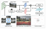
The paper details extensive experimentation that identified a bug in the RISC-V CVA6 Ariane core which had previously gone undetected. AutoSVA2 also allows the generation of Register Transfer Level (RTL) for a FIFO queue based on a fifty-word specification. To illustrate the process, here is an excerpt from the paper describing the workflow:
- Start with a high-level specification in English
- The LLM generates a first version of the RTL based on the specification, the module interface, and an order to generate synthesizable Verilog
- AutoSVA2 generates an FPV Testbench (FT) based on the RTL
- JasperGold evaluates the FT
- The engineer audits and fixes the SVA
- The LLM generates a new version of the RTL after appending the SVA to the previous prompt.
- Steps 3 to 6 are then repeated until convergence: either (a) full proof and coverage of the FT or(b) a plateau in the improvements of the RTL and SVA.
This process differs significantly from the role of a designer or verification engineer. GPT-4 creativity allows it to generate SVA from buggy RTL as well as create buggy SVA for correct RTL; reproducibility presents a challenge; internal signals, timing, syntax, and semantics may be partially incorrect and are partly corrected by the rules mentioned above.
On the positive side, AutoSVA2-generated properties improved coverage of RTL behavior by up to six times over AutoSVA-generated ones with less effort and exposed an undiscovered bug. The authors think that the approach has the potential to expand the adoption of FPV and pave the way for safer LLM-assisted RTL design methodologies. The Times They Are A-Changin’?
Also Read:
Perspectives from Cadence on Data Center Challenges and Trends
Designing and Simulating Next Generation Data Centers and AI Factories