You are currently viewing SemiWiki as a guest which gives you limited access to the site. To view blog comments and experience other SemiWiki features you must be a registered member. Registration is fast, simple, and absolutely free so please, join our community today!
Roger Cummings is the CEO of PEAK:AIO, a company at the forefront of enabling enterprise organizations to scale, govern, and secure their AI and HPC applications. Under Roger’s leadership, PEAK:AIO has increased its traction and market presence in delivering cutting-edge software-defined data solutions that transform commodity hardware into high-performance storage systems for AI and HPC workloads.
Roger is a seasoned entrepreneur and business leader with a distinguished track record of driving growth, innovation, and market leadership. Specializing in application infrastructure and AI/ML technologies, Roger has consistently identified emerging opportunities and built organizations that establish market dominance in rapidly evolving industries. Over his career, Roger has successfully guided five early-stage companies through highly successful acquisitions, raising over $1 billion in funding to fuel their global expansion.
In addition to his executive roles, Roger is an advisory board member at DevNetwork and an advisor at High Alpha Innovation. He has co-authored several papers on go-to-market strategies, operational excellence, and AI application infrastructure, reflecting his thought leadership in the field.
Tell us about your company?
PEAK:AIO is a pioneering AI infrastructure company specializing exclusively in data storage solutions engineered for Artificial Intelligence workloads. Unlike legacy IT storage vendors, our solutions are built from the ground up to match AI innovators’ exact needs and skill sets in the healthcare, government, life sciences, and advanced research sectors. Our mission is to eliminate bottlenecks in AI development by delivering unmatched speed, simplicity, and scalability.
What problems are you solving?
AI projects today often struggle with data bottlenecks caused by legacy storage solutions originally designed for traditional IT workloads. These outdated systems are typically complex, slow, energy-inefficient, and poorly aligned with the requirements of modern AI workloads. PEAK:AIO directly addresses these issues by providing storage infrastructure specifically designed for AI, eliminating data throughput limitations and significantly improving efficiency. We deliver up to six times the performance in one-sixth of the footprint, using just a fraction of the energy compared to traditional IT storage solutions.
What application areas are your strongest?
We excel in sectors where rapid access to vast datasets is crucial for successful AI outcomes, notably healthcare, life sciences, government, and large-scale AI research. Our technology underpins many significant AI initiatives, including pioneering deployments within the UK’s NHS and cutting-edge research collaborations with renowned institutions such as Los Alamos National Labs (LANL).
What keeps your customers up at night?
AI innovators, including data scientists, researchers, and medical professionals, worry most about their ability to rapidly and reliably access massive datasets needed to train complex AI models. They fear data bottlenecks that slow their projects, escalate costs and inefficiently use energy. Furthermore, managing complex, legacy storage infrastructure is not their core competency. Our customers need solutions that offer powerful simplicity, high performance, and extreme reliability, which is exactly what PEAK:AIO delivers.
What does the competitive landscape look like and how do you differentiate?
The competitive landscape is primarily populated by traditional IT storage vendors, which have adapted legacy solutions to attempt to meet AI needs. These repurposed offerings are usually complex, costly, and energy-intensive.
PEAK:AIO differentiates through purpose-built architecture optimized explicitly for AI workloads, delivering industry-leading performance, significantly lower energy use, and an unparalleled simplicity that fits the persona of today’s AI leaders, who are often highly skilled researchers and scientists who demand solutions that just work.
What new features/technology are you working on?
We are actively expanding our technology leadership by integrating advanced memory and storage architectures, such as CXL (Compute Express Link) and next-generation NVMe solutions, into our platforms. Additionally, we’re advancing our proprietary software-defined storage engine, designed to dynamically adapt storage tiers based on real-time AI workloads, continuously ensuring optimal performance and efficiency.
Additionally, we are evaluating vector database technologies and how this will help our clients.
How do customers normally engage with PEAK:AIO?
Customers typically engage through partnerships. We collaborate closely with each partner and customer to understand their specific AI infrastructure needs, and our specialist team provides personalized guidance, installation support, and ongoing optimization. This high-touch, expert-led engagement ensures our customers gain the maximum value and performance from their AI investments.
In this episode of the Semiconductor Insiders video series, Dan is once again joined by Anna Fontanelli, founder and CEO of MZ Technologies. In this discussion, more details of the challenges presented by advanced packaging and multi-die design are explored. Anna provides details of what’s involved in architectural exploration and interconnect management. She also provides some background on how MZ Technologies helps tame these challenges with its GENIO EVO platform.
The views, thoughts, and opinions expressed in these videos belong solely to the speaker, and not to the speaker’s employer, organization, committee or any other group or individual.
The TSMC Technology Symposium recently kicked off in Santa Clara, with a series of events scheduled around the world. This event showcases the latest TSMC technology. It is also an opportunity for TSMC’s vast ecosystem to demonstrate commercial application on TSMC’s technology. There is a lot to unpack at an event like this. There are great presentations and demonstrations everywhere, but occasionally a company rises above the noise and grabs the spotlight with unique or memorable news.
My view is that Analog Bits stepped into the spotlight this year with cutting-edge analog IP on the latest nodes and a strategy that will change the way design is done. Let’s examine how Analog Bits steals the show with working IP on TSMC 3nm and 2nm and a new design strategy.
Blazing the Trail to 2nm
Working silicon demonstrations of TSMC’s CLN2P technology represent rare air at this TSMC event. Analog Bits recently completed a successful second test chip tapeout at 2nm, but the real news is the company also came to the show with multiple working analog IPs at 2nm. Six precision IPs were demonstrated, the locations of those blocks on the test chip is shown below and the finished chip pictured at the top of this post.
ABITCN2P – Test Chip Layout
What follows are some details from the cutting edge. Let’s begin with the wide range PLL. Features of this IP include:
Electrically programmable for multiple applications
Wide range of input and output frequencies for diverse clocking needs
Implemented with Analog Bits’ proprietary architecture
Low power consumption
Spread spectrum tracking capability
Requires no additional on-chip components or bandgaps, minimizing power consumption
Excellent jitter performance with optimized noise rejection
The figure below illustrates some power and jitter numbers. Note the jitter data is for the whole test setup, test chip output buffers, test board, measurement equipment, and not a de-embedded number of the PLL standalone.
PLL Jitter and Power
Next is the PVT sensor. IPs like this are critical for managing power and heat. There will be more on power management in a bit. Features of this IP include:
High accuracy thermometer is a highly integrated macro for monitoring temperature variation on-chip
Industry leading accuracy untrimmed, with easy trimming procedures
An additional voltage sample mode is included allowing for voltage monitoring
The block includes a simple-to-use digital interface that works with standard core and IO level power supplies
Implemented with Analog Bits’ proprietary architecture
Low power consumption
Demonstrations included showcasing the temperature accuracy and temperature and voltage linearity of the IP.
Next is a droop detector. Voltage droop is another key item for power management. It occurs when the current in the power delivery network (PDN) abruptly changes, often due to workload fluctuations. This effect can lead to supply voltage drops across the chip which can cause performance degradation, reduce energy efficiency, and even result in catastrophic timing failures. Feature of this IP include:
Integrated voltage reference for stand-alone operation
Easy to integrate with no additional components or special power requirements
Easy to use and configure
Programmable droop detection levels
Low power
Implemented with Analog Bits’ proprietary architecture
Requires no additional on-chip macros, minimizing power consumption
The next IP is an 18-40MHz crystal oscillator. Features for this IP include:
Pad macro that supports most industry standard crystals in the 18-40MHz range
Uses standard CMOS transistors
Power-down option for IDDQ testing
Oscillator by-pass mode option for logic testing
Self-contained ESD protection structure
And finally, the differential transmit (TX) and receive (RX) IP blocks. Features here include:
TX
Wide frequency range support up to 2,000 MHz output for diverse clocking needs
Implemented with Analog Bits’ proprietary architecture
Low power consumption
Requires no additional on-chip components or bandgaps, minimizing power consumption
RX
Differential clock receiver
Single-ended output to chip core
Wide ranges of input frequencies for diverse clocking needs
Implemented with Analog Bits’ proprietary architecture
Low power consumption
Programmable termination
Spread spectrum tracking capability
Requires no additional on-chip components or bandgaps, minimizing power consumption
On the Cutting Edge with 3nm IP
Four power management IPs from TSMC’s CLN3P process were also demonstrated at the show. The test chip these IPs came from is also pictured in the graphic at the top of this post. The IPs demonstrated include:
A scalable low-dropout (LDO) regulator. Features of this IP include:
Integrated voltage reference for precision stand-alone operation
Easy to integrate with no additional components or special power requirements
Easy to use and configure
Scalable for multiple output currents
Programmable output level
Trimmable
Implemented with Analog Bits’ proprietary architecture
Requires no additional on-chip macros, minimizing power consumption
The line regulation performance of this IP is shown in the figure below.
Next is a spread spectrum clock generation PLL supporting PCIe Gen4 and Gen5. Features of this IP include:
High performance design emphasis for meeting low jitter requirements in PCIe Gen4 and Gen5 applications
Implemented with Analog Bits’ proprietary LC architecture
Low power consumption
Spread spectrum clock generation (SSCG) and tracking capability
Excellent jitter performance with optimized noise rejection
Calibration code and bandgap voltage observability (for test)
Requires no additional on-chip components, minimizing power consumption
A high-accuracy thermometer IP using Analog Bits patented pinless technology was also demonstrated. Features of this IP include:
IP is a highly integrated macro for monitoring temperature variation on-chip
Industry leading accuracy untrimmed, with easy trimming procedures
An additional voltage sample mode is included allowing for voltage monitoring
The block includes a simple-to-use digital interface that works with just standard core and power supply saving customers analog routing and simplifying package design
Pinless technology means the IP is powered by the core voltage, no analog power pin is required
Low power consumption
Voltage linearity for this IP is shown in the figure below.
Voltage Linearity
And finally, a droop detector for 3nm. Features include:
Integrated voltage reference for stand-alone operation
Easy to integrate with no additional components or special power requirements
Easy to use and configure
Programmable droop detection levels
Low power
Implemented with Analog Bits’ proprietary architecture
Requires no additional on-chip macros, minimizing power consumption
Intelligent Power Architecture Launches a New Design Strategy
Innovation brings new challenges. A big design challenge is optimizing performance and power in an on-chip environment that is constantly changing, is prone to on-chip variation and is faced with all kinds of power-induced glitches. As multi-die design grows, these problems are compounded across many chiplets that now also need a high-bandwidth, space-efficient, and power-efficient way to communicate.
This problem cannot be solved as an afterthought. Plugging in optimized IP or modifying software late in the design process will not be enough. Analog Bits believes that developing a holistic approach to power management during the architectural phase of the project is the only path forward.
It is against this backdrop that the company announced its Intelligent Power Architecture initiative at the TSMC Technology Symposium. The company stated that its high-accuracy on-die PVT sensors, process performance monitors, integrated power-on resets, droop detectors, LDOs, and glitch catchers all work together with its low power SerDes, ADCs and pinless IP libraries to deliver a power management architecture that will meet the most demanding requirements. Pinless IP technology, invented by Analog Bits, will become even more critical to migrate below 3nm as all of the IP will work directly from the core voltage. The technology is already proven in production silicon on N5 and N3.
Analog Bits stated the company is already working with large, successful organizations that are building some of the most power-hungry chips in the world to achieve this goal. The mission now is to bring an intelligent power architecture to mainstream design for all companies. This work will be interesting to watch as Analog Bits re-defines the way advanced design is done.
Keep watching the company’s website as the strategy behind the Intelligent Power Architecture unfolds. And that’s how Analog Bits steals the show with working IP on TSMC 3nm and 2nm and a new design strategy.
Dan is joined by GP Singh, CEO of Ambient Scientific. With over 20 years of experience, GP has played a pivotal role in shaping the industry, driving 50+ chip tapeouts, including game-changing advancements at FinFET technology nodes. Now, as the CEO of Ambient Scientific, GP brings together hands-on engineering expertise and visionary leadership, with more than 50 patents and 5 publications to his name.
In this highly informative and very relevant discussion, GP explains some of the fundamental obstacles to large-scale deployment of AI in both the datacenter and at the edge. A primary issue today is that AI circuits are either too limited in capability or too power hungry. GP describes the genesis of a unique approach to this problem developed by Ambient. He explains that the approach is to use analog AI compute, but to create a hybrid analog/digital architecture that delivers high performance at low power.
Ambient has plans to deliver applications on top of its silicon technology but customers can also build applications as well, creating a very wide footprint in the market. The impact of this enabling technology can be quite substantial.
The views, thoughts, and opinions expressed in these podcasts belong solely to the speaker, and not to the speaker’s employer, organization, committee or any other group or individual.
In the early days of RISC-V adoption, applications were microcontroller-centric with no need for virtualization support. But horizons expanded and now RISC-V is appearing in application processors, very much needing to be able to virtualize multiple apps concurrently. Take another step forward to datacenter servers running virtual machines under hypervisors, with each virtual machines running multiple virtual processes. Virtualization is turning up everywhere in RISC-V, supported by a standard for the MMU that virtualization requires. But the complexity of the standard is taxing verification teams when it comes to developing comprehensive testplans. I talked to Adnan Hamid (President and CTO) and Dave Kelf (CEO) of Breker Verification to get insight.
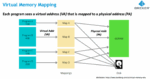
A quick recap on virtual memory and MMUs
The basic idea is quite simple. Each software developer can assume their program is running standalone with as much memory as it needs. The operating system (and the MMU) supports this fiction through an indirection between virtual and physical memory. This memory space indirection allows the OS/MMU to allocate and move around chunks of memory in the form of pages to support multiple processes occupying physical memory and/or offline storage at the same time. Virtualization delivers multiple benefits: More than one program can be active at a time; Each program can assume it has access to more memory than is physically available since overflow can be swapped out to disk; the OS/MMU can transparently optimize to reduce memory fragmentation as running processes complete; the OS/MMU can ensure memory isolation between processes, so if one process tries to access an out-of-bounds address in its own space, that attempt doesn’t affect other processes running at the same time.
Hypervisors add another level of indirection. These run multiple virtual machines, each in their own virtual space hosting an OS with services, in turn running multiple virtualized processes within that virtualized space. Nothing really complicated there.
Where it gets complicated
Seems pretty straightforward, right? Unfortunately it gets a whole lot more tangled in the details. MMU complexity isn’t unique to RISC-V. Adnan has previously worked on MMU verification for x86 and Arm-based systems and confirms there is plenty of complexity in both. Still, the RISC-V definition is unique in a few ways. First, the definition was finalized more recently, implying perhaps more time is needed for the standard (or at least documentation of the standard) to fully mature through widespread deployment. Second, in keeping with the RISC-V philosophy, MMU support is defined through extensions to the ISA, but the compatibility test framework requires demonstrating system level compatibility between multiple processors, probably coherent networks, the MMU, external memory and backing store. Third, the RISC-V standard teams saw opportunity to further generalize the definition, no doubt adding more capability but also more complexity.
Some of the complexity is just in the nature of MMUs. Process image data is stored in pages, each page 4KB by default but different profiles allow for larger pages, even a mix of page sizes. Pages are indexed by page tables, a lookup mechanism storing virtual and physical offsets for each page in memory. When a read or store is made to an address, the MMU will attempt to find the corresponding reference in these page tables. Naturally this lookup is supported by a cache (TLB) to enhance performance. If the appropriate address is already in a page in memory, the value can be returned/updated. If not, the MMU faults through to finding the appropriate page in main memory or backing store, bringing it in and making space by evicting some least recently used page currently in memory. When a hypervisor is active, lookup must go through two tables of indirection.
Add to this multiple levels of page table to accelerate lookup, multiple address translation protocols, privilege management, and other goodies which play into the details of how the MMU should function to be compatible with the RISC-V compliance tests. There is a written specification which Adnan repeatedly called “dense”, meaning long and complex. No doubt very carefully thought through by experts, though there still seems to be some debate about whether it is fully finalized.
Fairly quickly I get out of my depth in all this complexity. Instead I’ll turn to my own level of indirection by talking about what Breker has been doing to help DV teams in this space. Industrial experience in working with the standard is a pretty good indicator of maturity. One important point to remember is that the standard defines ISA extensions for MMU support, and it provides a system compatibility reference checker. It doesn’t tell you how to build your MMU or how to verify it. Both are left as exercises for the design and verification teams.
Breker SystemVIP for MMU verification
Breker hosted a tutorial on MMU testing at DVCon which was well attended (90 people). So popular that they have subsequently repeated the tutorial, reaching similar crowds. The tutorials reinforce that DV experts are struggling to know how to write testplans around MMUs for RISC-V-based systems.
Breker has put a lot of work into understanding these requirements to build a system VIP which can provide a canned starting point for DV testplans and test implementation. Adnan freely confesses that they aren’t all the way there yet. In Breker’s own work and in talking with clients, they know of holes in the Breker solution. Adnan says they have frequent and spirited discussions around whether the Breker interpretation is correct on any given point. At this point Adnan feels that the Breker has it right more often than not, but they still consider feedback both to test and to drive refinements to their implementation. Meantime clients and prospects keep coming back to Breker, with questions and arguments. A pretty good indication that even if incomplete, Breker is still leading the pack!
Very interesting. MMU system testing in the RISC-V world may be a niche but it’s a very important niche for anyone building a system which claims to support virtualization. You can learn more about Breker work in this space HERE.
VSORA AI Processor Raises $46 Million to Fast-Track Silicon Development
We stand on the cusp of an era defined by ubiquitous intelligence—a stone’s throw from a tidal wave of AI-powered products underpinned by next-generation silicon. Realizing that future demands nothing less than a fundamental rethink of how we design semiconductors and architect computers.
At the core of this transformation is a simple—but profound—shift: AI silicon must be shaped by AI workloads from day one. Gone are the days when hardware and software evolve in parallel—and only converge at validation, by which point the architecture is set in stone. Today’s paradigm demands re-engineer engineering, i.e., software-defined hardware design, tightly integrating AI code and silicon from the ground up.
Brute Force, No Grace: GPUs Hit the Memory Wall Processing LLMs
Today, the dominant computing architecture for AI processors is the Graphics Processing Unit (GPU). Originally conceived in 1999, when Nvidia released the GeForce 256 marketed as the “world’s first GPU”, it addressed the growing demand for parallel processing in rendering computer graphics. The GPU has since been repurposed to handle the massive, highly parallel workloads required by today’s AI algorithms—particularly those based on large language models (LLMs).
Despite significant advancements in GPU theoretical throughput, GPUs still face fundamental limitations, namely, poor computational efficiency, high power consumption, and suboptimal latency. To exemplify, a GPU with a theoretical peak performance of one PetaFLOPS and a realistic efficiency of 10% when processing a state-of-the-art LLM such as GPT-4 or LLM3-405B (noting that efficiency varies depending on the specific algorithm), would in practice deliver only 100 TeraFLOPS. To achieve a sustained PetaFLOPS of performance, 10 such GPUs would be required resulting in substantial more power consumption than that of a single device. Less apparent, this configuration also introduces significantly longer latency, compounding the inefficiencies.
Peeling back the layers of a GPU would uncover the culprit behind its poor efficiency: the memory wall. This long-standing bottleneck arises from an ever-widening gap between the insatiable demand of compute cores for data and the finite bandwidth of off-chip memory. As a result, cores frequently stall waiting on data transfers, preventing sustained utilization even when computational resources are plentiful.
Enhancements to the memory bandwidth via layered access in the form of multi-level caches have helped mitigate the impact—until the advent of AI workloads exposed this limitation. GPU’s brute-force approach, necessary to handle large language models (LLM), comes at a price: poor efficiency resulting in high energy consumption and long latency.
While GPU limitations during LLM training primarily manifest as increased computational cost, they pose a more critical obstacle during inference. This is especially pronounced in edge deployments, where stringent power budgets and real-time latency requirements, crucial for applications like autonomous driving, severely restrict GPU viability.
The VSORA Solution: Knocking Down the Memory Wall
While the semiconductor industry is intensely focused on mitigating the memory bandwidth bottleneck that plagues LLM inference processing, French startup VSORA has quietly pioneered a disruptive solution. The solution represents a paradigm shift in memory management.
VSORA Architecture: Functional Principles
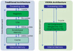
The VSORA’s architecture redefines how data is stored, moved, and processed at scale. At its heart lies an innovative scalable compute core designed around a very fast tightly-coupled-memory (TCM).
The TCM functions like an expansive and vast register file—offering the lowest-latency, single-cycle read/write access of any on-chip memory. Placed directly alongside the compute fabric, it bypasses the multi-cycle penalties of conventional cache hierarchies. As a result, VSORA maintains exceptionally high utilization even on irregular workloads, since hot data is always available in the very next cycle.
Together, the compute logic and the TCM form a unified, scalable compute core that minimizes data-movement overhead and bypasses traditional cache hierarchies. The result is an order-of-magnitude reduction in access latency and blazing-fast end-to-end inference performance across edge and data-center deployments. See figure 1.
Figure 1: Traditional hierarchical-cache memory structure vs VSORA register-like memory approach [Source: VSORA]
VSORA Architecture: Physical Implementation
The VSORA architecture is realized using a chiplet-based design within a 2.5D silicon‐interposer package, coupling compute chiplets to high-capacity memory chiplets. Each compute chiplet carries two VSORA basic compute cores, and each memory chiplet houses a high-bandwidth memory stack. Compute and memory chiplets communicate over an ultra-low-latency, high-throughput Network-on-Chip (NoC) fabric.
In the flagship Jotunn8 device, eight compute chiplets and eight HBM3e chiplets are tiled around the central interposer, delivering massive aggregate bandwidth and parallelism in a single package.
In most AI accelerators today, the fundamental compute element is a single-bit multiply-accumulate (MAC) unit. Thousands—or even hundreds of thousands—of these MACs are woven together in a massive array, with both the compiler and the user defining how data flows spatially across the array and in what temporal order each operation executes. While this approach excels at raw throughput for uniform, fixed-precision workloads, it begins to fracture under the demands of modern large language models and cutting-edge AI applications, which require:
Mixed-precision support: LLMs often need to employ different quantization on different layers, for example, a mix of FP8 Tensorcore, FP16 Tensorcore and FP16 DSP layers within the same network to balance performance, accuracy and numerical fidelity. This requires the system to repeatedly quantize and dequantize data, introducing both overhead and rounding error
Dynamic range management: Activations and weights span widely varying magnitudes. Architectures built around a single bit can struggle to represent very large or very small values without resorting to costly software-driven scaling.
Irregular and sparse tensors: Advanced workloads increasingly exploit sparsity to prune redundant connections. A rigid MAC mesh, optimized for dense operations, underutilizes its resources when data is sparse or when operations deviate from simple dot products.
These limitations introduce bottlenecks and reduce accuracy, consequently throughput drops when precision conversions don’t map neatly onto the MAC fabric, and critical data must shuffle through auxiliary units for scaling or activation functions.
VSORA’s architecture flips the script on traditional accelerator fabrics by adopting reconfigurable compute tiles that adapt on the fly—zero downtime, zero manual reprogramming. Instead of dedicating large swaths of silicon to fixed-function MAC arrays or rigid tensor cores, each VSORA tile can instantly assume either DSP-style or Tensorcore-style operation, at any precision (FP8, FP16, INT8, etc.), on a per-layer basis.
In practice, this means that:
Layer-optimal precision: One layer might run at FP16 with high-dynamic-range DSP operations for numerically sensitive tasks, then the very next layer switches to FP8 Tensorcore math for maximum throughput—without any pipeline stalls.
Resource consolidation: Because every tile can serve multiple roles, there’s no idle silicon stranded when workloads shift in precision or compute type. VSORA sustains peak utilization across the diverse math patterns of modern LLMs.
Simplified compiler flow: The compiler’s task reduces to choosing the ideal mode per layer—Tensorcore or DSP—instead of wrestling with mapping data to dozens of discrete hardware blocks.
The result is an accelerator that tunes itself continuously to each model’s needs, delivering higher accuracy, lower latency, and superior energy efficiency compared to static, single-purpose designs.
The VSORA’s architecture is not just about raw bandwidth; it’s about intelligent data processing, tailored to the specific demands of each application. This meticulous attention to detail at the core level is what distinguishes VSORA, enabling them to deliver AI inference solutions that are both powerful and efficient.
VSORA’s Secret Weapon: The Intelligent Compiler
Hardware ingenuity is only half the equation. VSORA’s algorithm-agnostic compiler consists of two stages. A front-end graph, hardware-independent compiler, ingests standard model formats (Tensorflow, PyTorch, ONNX, etc.) and optimizes the model via layer fusion, layer re-ordering, weight compilation and scheduling, slicing, tensor layout optimization, execution scheduling and sparsity enabling (data and weights). A back-end, LLVM-based compiler, fully automates the mapping of leading-edge LLMs—such as Llama—onto the VSORA J8.
VSORA’s architecture radically simplifies the deployment of large language models by replacing the tedious, error-prone mapping workflows common in GPU environments with an automated, software-defined memory management layer. Unlike traditional GPU toolchains—where developers must hand-tune data layouts, manage low-level memory transfers, and master platform-specific APIs such as NVIDIA CUDA—VSORA’s compiler handles all of this transparently. As a result, teams can bring LLMs online far more quickly and reliably, even in power-constrained or latency-sensitive applications, without sacrificing performance or requiring deep hardware-level expertise.
The result is a seamless compilation software stack that maximizes chip utilization, simplifies deployment, and unleashes the full performance potential of VSORA’s breakthrough inference platform.
Conclusion
Unlike general-purpose accelerators optimized for training, VSORA conceived an architecture optimized for inference. The specialization reduces latency, boosts real-world responsiveness, and drives down operational costs in scenarios where every millisecond counts—from on-device AI in smart cameras to safety-critical systems in self-driving cars.
Market research forecasts AI inference revenue to double from about $100 billion in 2025 to an estimated $250 billion by 2030—a 15+ percent compound annual growth rate. As enterprises race to deploy real-time AI at scale, VSORA’s efficiency-first approach could redefine cost structures and performance benchmarks across the industry.
On April 27, 2025, VSORA announced a $46 millions investment led by Otium Capital and a prominent French family office, with participation from Omnes Capital, Adélie Capital, and co-financing by the European Innovation Council Fund. In the words of Khaled Maalej, VSORA founder and CEO, “this funding empowers VSORA to tape-out the chip and ramp up production.”
Intel’s historical dominance in semiconductor process technology began to erode around 2018, as competitors started delivering higher performance at smaller nodes. In response, Intel is now doubling down on innovation across two fronts: advanced process nodes such as Intel 18A and 14A, and cutting-edge packaging technologies.
Interestingly, this emphasis on packaging innovation isn’t a deviation from Moore’s Law—it’s an expansion of it. In the original paper that gave birth to Moore’s Law, Gordon Moore wrote that it may prove economical to build large systems out of smaller functions, which are separately packaged and interconnected. That concept is materializing today through multi-die architectures and chiplet-based integration, which are key to Intel’s packaging roadmap.
These dual pillars of process and packaging took center stage at the recent Intel Foundry Direct Connect event, where Intel outlined how these technologies will power next-generation products in a world increasingly defined by AI-driven workloads and heterogeneous computing.
A separate article covers what was shared regarding advanced process and packaging technology. During Day 2 of the Direct Connect event, Walter Ng, VP of Worldwide Business Development at Intel Foundry Services, and TJ Lin, President of UMC-USA, gave a joint talk. This article focuses on that session.
The Cultural Challenge: From Products to Services
Technology alone is not enough to reinvent Intel’s role in the industry. A transformation from a product-centric company to a customer-focused foundry demands an equally profound cultural shift. For decades, Intel has engineered and delivered its own products; now, it must serve as a platform for others’ innovations. This shift was a major theme at the event, especially during the joint presentation by Intel and its strategic foundry partner, United Microelectronics Corporation (UMC).
UMC’s own evolution from an IDM (Integrated Device Manufacturer) to a dedicated foundry equips it with a culture deeply rooted in customer collaboration, operational efficiency, and service orientation. These are exactly the qualities Intel must adopt to succeed in its foundry ambitions—and UMC is well-positioned to help guide that transformation.
A Strategic Opportunity
While Intel is forging ahead on advanced process and packaging fronts, the 12nm process node was selected for the Intel-UMC partnership for several strategic reasons. Although future collaborations may include additional nodes, the immediate focus is on delivering a competitive 12nm platform that targets a broad range of applications: high-performance computing, mobile, RF, consumer, industrial, automotive, aerospace, and medical sectors.
This market is expected to grow to $20 billion by 2028, with early momentum driven by logic and RF designs. From 2027 onward, growth in specialty technologies is expected. Application areas include WiFi combo chips, RF transceivers, image signal processors, set-top box SoCs, and more—addressing the full spectrum of modern semiconductor demands.
Distributed Development and Accelerated Execution
Development is proceeding in parallel at UMC’s Tainan facility in Taiwan and Intel’s Ocotillo Technology Fabrication (OTF) site in Arizona, reinforcing a geo-diversified manufacturing strategy. With fabs across the US, Taiwan, Korea, China, EMEA, and Japan, the collaboration supports customers in building resilient, multi-sourced supply chains.
Initial performance benchmarks are promising: compared to UMC’s 22uLP node, the new 12nm offering delivers 28% better performance, 47% lower power consumption, and over 50% area savings. In response to anchor customers, Intel has accelerated its Process Design Kit (PDK) delivery schedule, enabling earlier design-in and tape-out.
The partners are also closely coordinating foundry operations and support services to ensure a seamless transition from design to high-volume manufacturing.
UMC’s Role and Expertise
UMC brings decades of experience in foundry operations, with a comprehensive ecosystem of IP and design enablement tools, support for specialty devices, and a diverse global customer base. Its track record in delivering complex, customized solutions makes it a strong partner in applications where tailored performance is essential.
Intel’s Added Value
Intel contributes significant R&D depth in FinFET technology, established advanced-node capacity, and leadership in packaging innovation. Initiatives like the Chiplet Alliance are enabling a robust ecosystem for modular system design. Furthermore, Intel’s domestic manufacturing footprint in the U.S. strengthens its appeal for customers with localization or national security requirements.
Together, Intel and UMC are offering a competitive FinFET solution that supports multi-sourcing strategies and provides a clear technology migration path for future products.
Service Culture Learning as a Catalyst for Change
Beyond technological and operational synergies, this collaboration serves a more profound purpose in Intel’s evolution: accelerating its cultural transformation. UMC’s journey from IDM to foundry is now becoming part of Intel’s learning curve. As Intel adopts a more customer-first mindset, this partnership offers valuable guidance and real-world insight.
The collaboration is not merely an exchange of capabilities; it is also a transfer of values, principles, and best practices that may shape the long-term success of Intel Foundry Services.
Summary
In a semiconductor industry defined by diversification, specialization, and global complexity, the Intel-UMC 12nm partnership exemplifies smart, strategic collaboration. By combining UMC’s mature process expertise with Intel’s FinFET and packaging leadership—alongside a deepening cultural alignment—the partnership is well-positioned to unlock new market opportunities.
As Intel seeks to reclaim its role as a technology leader and establish itself as a next-generation foundry platform, this collaboration with UMC isn’t just strategic—it’s foundational.
First used in the IBM 360 and now central to modern CPUs, speculative execution boosts performance by predicting instruction outcomes. Dr. Thang Tran’s predictive execution model charts a simpler, more efficient path forward.
By Dr. Thang Minh Tran, CEO/CTO Simplex Micro
In the world of modern computing, speculative execution has played a pivotal role in boosting performance by allowing processors to guess the outcomes of instructions ahead of time, keeping pipelines full and reducing idle cycles. Initially introduced during the development of the IBM 360 series in the 1960s, speculative execution helped break through the barriers of earlier architectures, enabling better CPU performance.
However, as computing demands have grown, so too have the problems caused by speculative execution. While it was a necessary innovation in the past, speculative execution has evolved into a complex, resource-hungry solution that now contributes to inefficiencies in modern processors. The need for continued patching to address its shortcomings has led to a sprawling web of fixes that add to power consumption, security risks, and memory inefficiencies.
The Legacy of Speculative Execution
From the early days of the IBM 360 to modern processors, speculative execution has been a cornerstone of processor architecture. Its ability to predict instructions before they are needed allowed for increased speed and reduced idle time in early systems. However, the cost of continuing to rely on this strategy is becoming increasingly apparent.
As processors have evolved, the complexity of speculative execution has grown in lockstep. Branch predictors, reorder buffers, load-store queues, and speculative memory systems have all been layered on top of each other, building a complicated and often inefficient architecture designed to “hide” the mispredictions and errors that result from speculative execution. As a result, modern CPUs still carry the weight of speculative execution’s legacy, creating complexity without addressing the fundamental inefficiencies that have surfaced in recent years.
The Hidden Costs of Speculation
While speculative execution offers a theoretical performance boost, the reality is more complex. There are significant costs in terms of silicon area, power consumption, and security vulnerabilities:
Silicon Overhead: Around 25–35% of a modern CPU’s silicon area is dedicated to structures that support speculative execution. These areas are consumed by components such as branch predictors, reorder buffers, and load-store queues (TechPowerUp Skylake Die Analysis).
Power Consumption: Studies from UC Berkeley and MIT suggest that up to 20% of a CPU’s energy is consumed by speculative execution activities that ultimately get discarded, adding a substantial energy overhead (CPU Power Consumption Study).
Security Penalties: The discovery of vulnerabilities like Spectre and Meltdown has shown that speculative execution can introduce serious security risks. Mitigations for these vulnerabilities have resulted in performance penalties ranging from 5–30%, particularly in high-performance computing (HPC) and cloud computing environments (Microsoft Spectre and Meltdown Performance Impact).
These overheads are not just theoretical. In practice, speculative execution leads to slower, more energy-intensive processors that also pose serious security risks—issues that have only become more pressing with the advent of cloud computing and AI applications that require efficiency at scale.
Looking Beyond Speculation: A Path Forward
The time has come for a new approach to CPU architecture, one that moves away from the heavy reliance on speculation. It’s clear that predictive scheduling offers a promising alternative—one that can achieve the same performance improvements without the waste associated with speculative execution.
Recent patented inventions in predictive execution models offer a glimpse of the future. By scheduling tasks based on accurate predictions of when work can begin, rather than relying on speculative guesses, it becomes possible to eliminate the need for rollback systems, avoid speculative memory accesses, and create a more efficient, secure architecture.
Conclusion: A Call to Action
In conclusion, the history of speculative execution shows us both the innovation it sparked and the limitations it has imposed. While speculative execution was a crucial step in the evolution of computing, the time has come to move beyond it. Recent patents filed on predictive execution provide a promising path forward, one that offers greater efficiency, security, and power savings for future architectures.
Let’s not just confirm the misery of the past decades but instead embrace a brighter future where CPU architectures can be both smarter and more efficient. The world is ready for a new era in computing—one that moves beyond speculation and into the realm of precision, predictability, and performance.
Intel, long a leader in semiconductor manufacturing, is on a determined journey to reclaim its technological leadership in the industry. After facing significant challenges in recent years, the company is making a concerted effort to adapt and innovate, with a clear focus on AI-driven technologies, advanced packaging solutions, and building a robust ecosystem.
During last week’s Intel Foundry Direct Connect event, Intel outlined its strategy and the investments it is making to enable this transformation. The company certainly does not intend to be encumbered by its recent history.
Transforming Intel Foundry: A Customer-Centric Approach
Intel is undertaking a significant transformation of its foundry business, with a renewed focus on becoming a customer-first, service-oriented organization. At the core of this strategy is a commitment to close collaboration with customers to ensure Intel not only meets, but anticipates their evolving needs. This transformation is guided by three strategic priorities:
Matching Technology to Customer Needs: Intel is aligning its technology offerings with the specific demands of industries like artificial intelligence (AI) and high-performance computing (HPC). Flexibility, predictability, and scalability are key pillars of this approach.
Improving Execution and Responsiveness: The company is refining its internal processes to better deliver on time and meet customer expectations with greater reliability.
Expanding the Ecosystem: Intel is investing significantly in ecosystem growth, including design enablement, IP support, and advanced packaging. These investments are designed to support its foundry business at scale.
Through these efforts, Intel aims to reshape its foundry operations into a comprehensive, end-to-end solutions provider equipped to meet the complex requirements of the modern semiconductor industry.
AI and Advanced Packaging: The Next Frontier
AI is transforming semiconductor design and manufacturing, and Intel is positioning itself as a foundational technology provider for this revolution. Recognizing that future computing performance relies not just on smaller transistors but also on smarter integration, Intel is making bold moves in advanced packaging.
Intel’s packaging technologies, including 2.5D and 3D solutions, are designed to offer increased design flexibility, faster time-to-market, and efficient performance scaling. Technologies such as Through-Silicon Vias (TSVs), embedded silicon bridges (E-bridges), and interconnect standards like UCIe are being implemented to address the demands of AI workloads—high bandwidth, low latency, and energy efficiency.
Intel’s EMIB (Embedded Multi-die Interconnect Bridge) enables high-density die-to-die connections in a 2.5D package without the need for a silicon interposer, offering cost and performance benefits for large chiplet-based designs. Foveros, Intel’s 3D stacking technology, allows different logic tiles to be stacked vertically, enabling heterogenous integration across process nodes. Foveros Direct, an evolution of this platform, introduces direct copper-to-copper bonding for ultra-high-density, low-resistance interconnects, pushing the boundaries of integration and energy efficiency.
The development of advanced solutions like HPM4 for high-performance memory and support for reticle-size packages up to 12X the standard, enable Intel to support large, AI-centric designs at scale.
A Collaborative Ecosystem: Strengthening Partnerships
Intel recognizes that its comeback won’t happen in isolation. Key to its strategy is building a robust, collaborative ecosystem. Lip-Bu Tan, CEO of Intel, underscored this during his talk, emphasizing the importance of ecosystem enablement to support AI’s massive growth.
Its leadership in forming the Chiplet Alliance, comprising over a dozen companies, highlights its effort to create a secure, standardized, and interoperable chiplet ecosystem. This initiative underlines Intel’s commitment to building a connected value chain across design, packaging, and manufacturing.
Intel is also partnering with United Microelectronics Corporation (UMC) to bring its 12nm technology to market, aimed at serving specialty applications. This collaboration leverages Intel’s manufacturing expertise with UMC’s strengths in design enablement. You can read about this on a separate post on SemiWiki: Intel’s Foundry Transformation: Technology, Culture, and Collaboration
The U.S. Government’s Role in Intel’s Vision
Intel views the U.S. government as a foundational partner in its mission to bring semiconductor leadership back to American soil. Programs like RAMP (Rapid Assured Microelectronics Prototyping) and the Secure Enclave Program are key enablers of trusted domestic manufacturing. These initiatives support the development and ramp-up of Intel’s cutting-edge 18A and 16 nodes, all of which will be manufactured in the U.S. Intel’s alignment with national security and economic priorities strengthens its position as both a commercial and strategic partner.
The government’s involvement is not just about funding—it’s about ensuring a resilient and secure semiconductor supply chain for both public and private sectors.
Summary
Intel’s strategy to regain technological leadership is built on four pillars: advanced process technology, next-generation packaging, ecosystem collaboration, and strong public-private partnerships. Looking ahead, Intel’s roadmap is anchored in technologies that provide scalable performance with predictable delivery.
With a customer-first mindset, a reinvigorated focus on execution, and a bold investment in innovation, Intel is poised to lead the next era of semiconductor technology.
Now that the dust has settled, I will give you my take on the Intel Foundry event. Some might call me a semiconductor event critic as I have attended hundreds of them over the last 40 years starting with the Design Automation Conference in 1984. Foundry events are my favorite because they really are the pulse of the semiconductor industry, it is all about the ecosystem of partners and customers. The message Intel Foundry sent this year is that they are going to earn your foundry business.
Last year, Intel Foundry was all about technology, which is fine, but what really matters is customers and that message was loud and clear to me this year. At some events I am herded around with media people but last week I ran free and was able to talk candidly with my fellow semiconductor professionals. More importantly, the badges were readable and mine even had my name on it in instead of just PRESS or MEDIA because I am so much more. I was amazed at the overall support by partners, pretty much everyone I saw at the TSMC event the previous week was there and quite a few badges from the top semiconductor companies were in attendance as well.
Surprisingly, the keynotes were live streamed which was a foundry event first for me. Speaking in front of more than a thousand of your peers AND live streamed? Horrifying if you think about it, and I have, but it was well done.
First up was Intel CEO Lip-Bu Tan. I have told people before that you should never bet against Lip-Bu. When he tells you something you can bank on it and that is my experience based on his time with Cadence. He first joined the Cadence board in 2004, was CEO 2009-2021, and left the board in 2023.
I started in the industry before there was a Cadence or Synopsys and spent the majority of my career in EDA and foundation IP. Cadence was having a very rough time when Lip-Bu joined and he turned Cadence into what they are today, a leading innovator in the semiconductor ecosystem.
Lip-Bu showed his EDA savvy by inviting EDA CEOs to the stage in a show of support on both sides. I have never seen this done before. It was amazing! Remember, without EDA companies there would be no foundries. Mike Ello did a nice job for Siemens EDA. I worked with Mike at Berkely DA up until the acquisition by Mentor. For those people who are concerned about Cadence having an inside advantage with Intel Foundry don’t be. Lip-Bu does not play that game. The foundry ecosystem has to be a level playing field and no one knows that better than Lip-Bu. On the EDA Enablement slide the key players were properly listed in alphabetical order: Ansys, Cadence, Keysight, Siemens EDA, and Synopsys.
Synopsys was nice enough to share some slides and a quote with me that really encapsulates what is going on with Intel 18A. I have heard this from multiple ecosystem people and customers so it is not just Synopsys and I agree 100% with Sassine Ghazi, CEO of Synopsys.
“You cannot only win with technology, you need to have the whole process of enablement ready in order for the customer to see it as viable,” said Sassine, holding an early Synopsys test chip produced on Intel 18A about one year ago. He also said the teams are now in early-stage DTCO for Intel14A-E, leveraging Synopsys Technology Computer-Aided Design (TCAD) to use computer simulations for process node development.
Speaking of 14A, Intel mentioned a while back that HNA-EUV will not be required for 14A and from what I understand the first foundry version of 14A will be EUV. TSMC has said the same and this is a very good thing if you remember when EUV was delayed for YEARS! As I always say, plan for the worst and hope for the best.
Second up was Naga Chandrasekaran, Intel Foundry chief technology and operations officer followed by Kevin O’Buckley, general manager of Foundry Services. I do not know Naga personally but I do know people who worked for him at Micron and they speak very highly of him. Naga is a strong leader. Kevin I do know and I can vouch for him, he is a true professional and will work well with Lip-Bu. Here is a 30 minute clip from the keynotes that is worth watching:
Bottom line: Even with the short amount of time he has been CEO, Lip-Bu has already made a difference. Just wait until next year. I would bet that the Intel Foundry 18A customer tape-out list will be the Who’s Who of the semiconductor industry, absolutely.