MediaTek is at crossroads. The company that pioneered the “Shanzhai” model for smartphones by providing small OEMs and ODMs in China with starter kits and turnkey design solutions is now facing its first real test after years of runaway success.
Continue reading “MediaTek: Where Do I Go From Here?”

Auto ISAC—What is it and do we need one?
An Information Sharing and Analysis Center (ISAC) is essentially a trusted entity established by critical infrastructure owners and operators to share threat data. ISACs first emerged in 1998 when President Clinton issued Presidential Decision Directive 63, which identified the nation’s critical infrastructure that could be attacked either through physical or cyber means.
The disruption of this critical infrastructure, such as banking and finance, the electricity generation and distribution network, drinking water and treatment facilities, would have a profound effect on the nation’s economic well-being. To address these risks, the federal government worked with each industry sector to establish a sector-specific organization to share information about threats and best practices for developing defenses.
Today, ISACs have been established within most of the critical infrastructure sectors and new ISACs continue to emerge as needed. For example, in the retail space where we’ve seen a series of high profile attacks against retailers such as Target and Home Depot, that industry recently established a retail ISAC, called the Retail Cyber Information Sharing Center.
So why do we need an Auto ISAC?
While there are a couple of transportation specific ISACs focused on protecting critical infrastructure, such as roads, bridges, rail, and mass transit, there isn’t an organization that focuses on the vehicles that use the roads and bridges. And frankly, there really wasn’t a need until more recently. Modern day automobiles are complex machines that can contain various embedded systems, interfaces, and networks. Furthermore, autos are increasingly featuring modems and other wireless capabilities. These wireless capabilities can support a host of features including remote tire pressure monitoring, navigation, telematics, and keyless entry and ignition start. The prospects of vehicle autonomy, self-driving capabilities, and Vehicle-to-Vehicle communications also promise tremendous benefits for efficiency, comfort, and driving safety which may be on the near horizon. The continuing trend in vehicle safety is shifting toward more interconnected systems and a reliance on sensors to identify hazards and take appropriate action.
All of these features are great and provide tremendous safety benefits, but these features also create new attack vectors that will undoubtedly increase the risk that these systems can be compromised. And when the many different systems become interconnected, then potentially really bad things can happen. While we have not seen any real world exploits of cyber-vulnerabilities in automobiles in the wild, we do know that with the increasing level of research, testing, and demonstration, it’s certainly possible to remotely take over control of a vehicle and override all driver inputs.
In 2010, researchers from UC San Diego and the University of Washington briefed NHTSA on their research. However, in order to reach out to the auto industry to disseminate their findings, the researchers would have to request meetings with the right people at each of the different auto manufacturers. One can imagine how time consuming and inefficient such a process could be.
Furthermore, those manufacturers who weren’t directly affected may not have been interested to learn about it (i.e. it’s not my problem). Had an Auto ISAC existed then, it would have been the logical and ideal place to present the discoveries. The ISAC could have analyzed the data and ensured that the proper representatives at the different manufacturers were properly informed. This specific use case, along with emerging risks that come with the many benefits of the increasing connectivity, complexity, and reliance on electronics, led NHTSA to encourage the auto industry to consider creating an auto industry specific ISAC.
ISACs have unique capabilities to provide comprehensive threat analysis within the sector and have the ability to reach out to other sectors and with government to share critical information. An Auto ISAC will help the industry share information to identify and analyze threats, vulnerabilities, and incidents specific to motor vehicles and serve as a resource to analyze potential impacts of such concerns to the sector. An Auto ISAC would also provide the industry with access to collective intelligence accumulated across the network of existing ISACs in other industry sectors, as well as potentially intelligence from the US government.
In July 2014, the Alliance of Automobile Manufacturers and the Association of Global Automakers sent a joint letter to NHTSA indicating that the industry’s intent to pursue the development of an Auto ISAC. The auto industry the started working on identifying the appropriate elements necessary to establish and maintain an Auto ISAC. Below are the seven major elements they identified.
[LIST=1]
Once this foundational work was complete, the auto industry announced in July that they would be launching the Auto ISAC. The Auto ISAC should be up and running in the coming months, and the timing couldn’t be better given the recent news about researchers remotely taking control of a vehicle.
Magwel’s Current Tools Take an Active Role in Power Transistor Design

It often seems that semiconductor industry coverage focuses on large digital markets like microprocessors or high frequency analog designs for RF applications. Yes, these are large markets, but power transistors like IBGT and VFETS make up a large and crucial sector. Not only do they make their way into discretes, but they are an important part of the mobile and IoT market where they are used for PMICs and a variety of high power and high voltage applications.
A power transistor is not a single junction but actually dozens or often thousands of parallel junctions operating in concert. Just as in digital circuits there is a premium on switching speed and coherence so that junctions are operating with the least resistance. Due to the large distributed nature of these devices, the parasitics from the metal and poly interconnect and gate and junction play a significant role in determining device performance. Engineers designing power transistors need to look at an extensive range of characteristics to fully model device behavior so they can optimize them.
Magwel is an EDA supplier that has made power transistor modeling one of its specialties. They offer a suite of tools known as PTM (Power Transistor Modeler) for addressing the needs of power transistor designers. Because I have been working with Magwel I have become much more familiar with these products.
One of the fundamental parameters of a power transistor is its drain-source resistance (Rdson). Magwel’s base PTM product predicts Rdson by combining linear or non-linear models for the junction when it is fully switched on with a detailed analysis of the metal and poly network connecting the source and drain terminals. This is a large network with many parallel paths, due to the large number of parallel active areas. To calculate this all the current paths are analyzed.
The user specifies the source and drain voltages or currents as fixed values or using excitation from a Voltage Controlled Voltage Source (VCVS) which is helpful for designing sense devices. The channel can be modeled linearly with a specified channel resistance or non-linearly to account for debiasing. PTM results include voltages, IR drop, resistance per layer and current densities, which are used to predict reliability information and to look for electro-migration violations.
PTM features a field viewer that shows voltage and current density overlaid on the layout. In addition to 2-D views, plots of the results from user selected 1-D cross-cuts can be generated. PTM also creates comprehensive reports in csv format for later analysis.
After Rdson, gate delay is one of the next most important factors determining device performance. PTM-GD uses a 64 bit mesh based solver to extract the distributed RC networks for the gate metal and poly interconnect up through the metal stack to the device terminals. To allow accurate and fast analysis PTM-GD uses distributed RC or distributed spice models to model the distributed nature of the gate network. SPICE is then used to compute the gate delay values.
So far we have been talking about steady state behavior, but modeling dynamic switching behavior provides an even better understanding of a power device. Magwel’s PTM-TR offers a view of the full transistor behavior over time. Using its visual feedback, designers can optimize switching performance to ensure faster and more uniform transitions across the device, minimizing power dissipation. This is especially useful for minimizing dead-time or shoot-through current in DC-to-DC converters.
PTM-TR produces a distributed model for the gate, drain and source networks. The active areas are segmented using SPICE derived table models so that the full switching behavior can be modeled in detail. At each time of interest during switching it is possible to see the voltages and currents across the device. This makes it possible to optimize the layout to provide more optimal switching minimizing dead-time, current crowding and shoot-through currents. For example, in the case of converters, it is possible to model high-side and low-side devices operating together to obtain a very accurate transient performance of the converter.
The final critical performance element is thermal behavior. High currents generate joule heating in the active areas and interconnect for the source and drain that in turn affect electrical properties of the device. Other external heat sources and sinks also play a factor in the thermal environment of the device. Using PTM-ET designers can fully define thermal sources and sinks in the package and even in the board. PTM-ET calculates thermal heating during operation by simultaneously solving the electrical and thermal equations for the circuit. Doing this fully considers the interdependency between thermal and electrical operation.
We all enjoy our mobile and battery powered devices, but without highly efficient power management circuits their battery life will disappoint, leaving us without their full benefits. Thus we find that optimal design for these circuits is paramount. Magwel’s Power Transistor Modeling suite offers a complete solution for ensuring optimal power transistor performance during all aspects of circuit design. For more information please visit the Magwel website at www.magwel.com.
mbed Evaluation Boards Showcase Focus on IoT Software, Connectivity
ARM’s mbed operating system is winning attention in the highly fragmented embedded software space by promising a solid software foundation for interoperable hardware and thus scale the Internet of Things (IoT) designs by narrowing the development time.
Continue reading “mbed Evaluation Boards Showcase Focus on IoT Software, Connectivity”
Academia and TCAD Grow Closer

On my first trip to Austria for EDA business I traveled by car from Germany, and I couldn’t wait to see how fast we would travel on the fabled Autobahn. Oddly enough it was summertime and the Autobahn was filled with vacationing families driving cars with shiny, aluminum campers in tow, so our car only traveled about 60 mph, nothing like the unlimited speeds that I’ve seen on YouTube. Located in Vienna, Austria is the TU Wien Institute for Microelectronics, a place where researchers focus on defining models, write software and create new tools for the simulation of both semiconductor devices and the technology processing steps (aka TCAD). To actually test out their ideas in silicon they partner with fabs and IDMs in Europe and around the globe. TU Wien has ongoing research in these five areas:
- Device Simulation
- Process Simulation
- High Performance Computing
- Meshing
- Very Large Scale Integration
The folks at TU Wien are now partnering with Silvacoto create the new Christian Doppler Laboratory (CDL) for High Performance TCAD, along with some financing provided by the Austrian Ministry of Science, Research and Economics. The CDL opened up just last month on October 5th and there’s a group photo taken at the official opening below.
I’m not certain how many American or other Universities are partnering with TCAD vendors, but the concept certainly makes a lot of sense because of how critical it is to design and optimize any new process technology prior to actual fabrication. Dr. Josef Weinbub will be heading up the new CDL, and he even has his own web site. He has been doing TCAD research since 2010, and has won an award from the NVIDIA GPU Research Center. I’m wondering if his involvement with GPUs may indicate that Silvaco will port a TCAD tool to work with GPUs, speeding up the time required for simulations.
The research team at CDL will be using Silvaco TCAD tools, and the close collaboration will certainly improve the features in these tools. Silvaco also has research sites in Grenoble, France and Cambridge UK. I often make the mistake of thinking that smaller EDA vendors are located in a single building, but with Silvaco they have people in North America, Europe, Japan and Asia. This partnership between academia and Silvaco looks like a good deal between science and business.
Here’s a list of TCAD tools that Silvaco offers to give you an idea of the breadth:
- 3D Device Simulator (Victory Device)
- Layout-driven 3D Process Simulator (Victory Process)
- Virtual Wafer Fab (VWF)
Related Blogs
Advances in DDR IP Solution for High-Performance SoCs
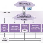
In this era of high-performance, low-power, and low-cost devices coming up at an unprecedented scale, the SoCs can never attain the ultimate in performance; always there is scope for improvement. Several methods including innovative technology, multi-processor architecture, memory, data traffic management for low latency, and software have been explored with great success in enhancing SoC performance. Continue reading “Advances in DDR IP Solution for High-Performance SoCs”
Samsung Versus Intel at 14nm
Daniel Nenni recently blogged about Intel’s claims of industry leading process density that were made at their analysts meeting. It isn’t clear to me why Intel makes this such a big focus at the analysts meetings, they really don’t compete with the foundries much but this seems to be a big deal to them. I thought it would be interesting to take a detailed look at Intel’s 14nm process and contrast it to Samsung’s 14nm process and put some of these claims in perspective. I picked Samsung because Samsung has the densest 14nm foundry process.
Dan’s blog is available here.
With 14nm parts now out in the market from both Intel and Samsung a lot is known about both processes, in fact I believe I have a good detailed understanding of both processes. In this article I am going to focus on the back end of line (BEOL) because I believe it really illustrates the differences in approaches.
Samsung 14LPE process
Samsung’s 14LPE process is a foundry process and as such it has to accommodate a wide variety of customer needs. The process offers 4 levels of minimum pitch metal (64nm). The minimum pitch metal layers at 64nm are below the single patterning limit of ~80nm and therefore require multi-patterning. Samsung has chosen to use litho-etch-litho-etch (LE2) where the pattern is broken up into two masks that are exposed and etched separately. There are advantage and disadvantages to LE2 as a multi patterning approach versus other approaches such a self-aligned double pattering (SADP). The big advantage to LE2 is that the pattern produced can be 2D with metal runs in both the X and Y directions; the disadvantage is that the achievable minimum pitch isn’t as small as it is with SADP. For a foundry process flexibility in metal routing is very important and trading off some pitch for routing flexibility makes sense.
The Samsung 14LPE process also employs self-aligned vias. Basically the LE2 metal pattern is done first and memorized into a hard mask and then the via pattern is overlaid. The via pitches are also relaxed and this allows the vias to be single patterned.
Intel P1272 process
Intel develops microprocessor processes first and then adapts the processes for foundry later (typically around a year later). Because Intel controls both the process and the design for their microprocessors it allows them to impose much stricter design rules than a foundry can typically require and the P1272 process is an excellent example of this. For the first four metal layers Intel has used SADP with block masks. SADP creates a mandrel and then spacers on the mandrel edges doubling the mask pitch. SADP can in theory double an 80nm single exposure mask to a 40nm pitch. The drawback is the 40nm pitch is only achieved in one direction basically creating parallel lines and spaces in that direction. You get tightly spaced lines in the X direction but no lines in the Y direction. The lines also have to be cut or in the case of interconnect blocked by one or more additional masks.
By using SADP Intel has achieved pitches of 56nm, 70nm, 52nm and 56nm for the first four metal layers. These are however 1D gridded lines and spaces allowing much less metal routing flexibility. In fact to some extent what was a single 2D metal layer has to be broken up into two 1D metal layers. This has resulted in a significant increase in the number of metal layers required for the 14nm process. Intel’s 130nm, 90nm, 65nm, 45nm, 32nm and 22nm processes had 6, 7, 8, 9, 9, and 9 metal layers respectively, at 14nm the metals layers jumped to 13!
The Intel P1272 process also utilizes self-aligned via so the critical via are single patterned.
Conclusions
After reading this you may wonder which BEOL is better and the answer is it depends. For Intel’s microprocessor designs where they can impose very strict design rules Intel has undoubtedly done an exhaustive analysis to decide on their process. For Intel, foundry is a distant second to microprocessors in priority and I would suspect the process decisions were heavily weighted towards optimizing it for microprocessors. For Samsung the 14LPE process is a foundry process and needs to support more flexible metal routing. Intel achieves a tighter pitch on individual metal layers but depending on the routing requirements this may or may not achieve a denser design or may require additional metal levels and therefore higher process costs.
See also Apple versus Zebras
Internet of Things in 2016
2015 was a big year for the Internet of Things (IoT). In our minds, it seems to have been the year nearly all big companies developed an IoT strategy. At the risk of sounding cliche, you could say IoT became mainstream in 2015.
Continue reading “Internet of Things in 2016”
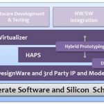
5 ways FPGA-based prototyping shrinks design time
Engineers are trained to think linearly, along the lines of we started here, then we did this, and that, and this other stuff, and here is where we ended up. If you’ve ever presented in an internal review meeting, sales conference, or a TED-like event, you know that is a dangerous strategy in winning friends and influencing people. Continue reading “5 ways FPGA-based prototyping shrinks design time”
The Fog Begins to Lift on 5G Cellular
5G mobile communication is widely forecasted to be a market reality seven to ten years from now. As envisioned by the International Telecommunications Union Radiocommunications sector (ITU-R), in their next generation International Mobile Telecommunication or IMT-2020 documents, 5G comprises three top-level goals: enhanced mobile broadband; massive machine type communications; and ultra-reliability and low latency communications. There are eight technical criteria which underpin these goals: peak data rate; user-experienced data rate; area traffic capacity; spectrum efficiency; network energy efficiency; mobility; connection density; and latency. The IMT-2020 manifesto sets daunting performance enhancement goals for each of these criteria that range from the geometric (such as a 3x increase in spectrum efficiency) to the exponential (such as a 100x increase in network energy efficiency).
The 3rd Generation Partnership Project (3GPP) standard setting organization, having successfully driven the 4G LTE / LTE-Advanced standards into more than 450 networks in about 140 countries worldwide, is starting to establish study items, to be followed by work items, for their Release 15 (5G Phase 1) and Release 16 (5G Phase 2) specifications targeted for 2018 and 2019, respectively. Research organizations in the US, Europe and Asia are actively investigating digital wireless communications and networking technology alternatives and enhancements, such as RF channel modeling above 6 GHz, non-orthogonal waveforms, and network slicing.
One area of relative clarity is the technical consensus that carrier frequencies above 6 GHz are almost certainly required to achieve the IMT-2020 peak data rate target benchmark of 20 Gbps and the user-experience data rate target benchmark of 100 Mbps. This month, the World Radiocommunication Conference 2015 is being held in Geneva. US FCC delegates to this conference are proposing five frequency bands for 5G services: 27.5 to 29.5 GHz; 37 to 40.5 GHz; 47.2 to 50.2 GHz; 50.4 to 52.6 GHz; and 59.3 to 71 GHz. This is a total of 22.4 GHz of potential new spectrum, enabling channels bandwidths up to 2 GHz. Obviously, the FCC must work diligently with other major international regulatory organizations to encourage globally harmonized 5G spectrum, in preparation for the next WRC meeting in 2019.
A little math reminds us that 5 GHz corresponds to 6 cm wavelength, and 30 GHz corresponds to 1 cm wavelength. Frequencies above 30 GHz are considered millimeter waves, and mm waves have significantly different propagation characteristics (such as free space loss, diffraction and delay spread) than cm waves below 6 GHz. Both atmospheric water vapor (peaking at about 22 GHz) and oxygen (peaking at about 63 GHz) absorb significant RF energy. While 60 GHz channel modeling has been conducted in the context of 802.11ad WiGIG, the 5G standardization process requires a more comprehensive effort. Recognizing this shortcoming, in March of this year, Nokia Networks put forward a 3GPP Work Item Description (RP-150308) to organize and unify the mm wave channel modeling effort, explicitly acknowledging the opportunity to leverage the research work currently underway outside the 3GPP.
One of the intriguing aspects of mm wave cellular is the potential for user equipment (i.e., smartphone) high order MIMO two dimensional antenna arrays. Cellular MIMO has been impractical on LTE smartphones largely due to the small physical dimensions of handheld devices, despite antenna innovations from SkyCross and others. On the infrastructure side, LTE eNodeB base stations since 3GPP Release 12 have included 2×2, 4×4, 8×8 single-user MIMO radio options with digital beamforming, and Release 14 supports eNodeB “full dimensional” (i.e., elevation and azimuth “pencil” beamforming) supporting dozens of multi-user MIMO client devices. With mm wave cellular, there is the potential to include an 8×8 array antenna in less than 40 square mm of area, small enough for use in 4.7″ screen size smartphones.
The relatively short range of mm wave cellular has led to a consensus view that 5G’s ambitious 5G peak and average data rates will be practically achievable only using small cell base stations addressing indoor high bandwidth use cases, such as streaming UHD video. Complementary to this view is the conception of 5G as overlay to existing 4G LTE-A networks, with enhancements to LTE-A, such as LTE-M (machine-to-machine) and LTE-U (unlicensed band) likely to be positioned by carriers as 4.5G.
There is much to anticipate with respect to cellular transceiver research and development in the coming decade!