It’s really challenging to reach design closure of an SoC by meeting timing constraints, staying within the power budget, tracking progress, communicating within the team, minimizing the floorplan, maximizing manufacturability and eliminating hotspots. Most SoC design teams have EDA tools from multiple vendors, and yet no single vendor has figured out a simple way to accomplish all of these objectives in an automated tool flow. These multiple challenges can be addressed, and in fact one company in particular has an EDA tool that does work with multiple point tools to distill data and analytics into design information. That company is Dassault Systemes, and their EDA tool is called ENOVIA Pinpoint.
Paul McLellan first blogged about PinPoint back in 2013, but there’s been a lot of progress since then in terms of new features. The Pinpoint tool provides both engineers and managers a dashboard-based system for design closure, and it uses analytics to help the team members debug closure issues more quickly than manually looking at gigabytes of EDA tool log files.
What’s New in Pinpoint
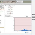
You can now easily analyze all of your SoC timing paths across all modes of operation and all corners using the Timing Scenario feature.
Timing on SoCs is dominated by interconnect, so knowing the capacitance values of your interconnect is critical to reaching timing closure. In Pinpoint there’s a timing DRC report for max trans and max cap which appear on your IC layout as red and orange colored circles.
Pinpoint works with all of the major EDA tools for static timing analysis, place and route, and IC layout. It even supports the Synospys PTPx power report and lets you visualize layout overlays based on leakage, internal and dynamic info taken from the Primetime static timing analysis tool.
There’s a new timing scenario mode summary that lets an engineer consider timing paths that span all modes and corners. You can now look at your timing paths that violate timing on most of your analysis points at once, instead of having to review each mode and corner one at a time.
SoC design managers will like using Pinpoint because it makes the whole team more efficient, especially during a design review meeting by presenting all the data quickly without having to create manual reports. Managers can start with a summary of how their project is tracking against schedule and then proceed to lower levels of detailed by just clicking. They will know where each block is at in getting to closure and the full-chip. Historical metrics tell you how the project is trending, and if its converging or not.
Design engineers get to spend more time designing and less time reporting because they have an environment that lets them collaborate with their entire team, creating a way for all engineers from RTL to physical keep in touch, and allowing anyone to make a comparison of all experiments tried so far.
Related Blogs
How Can Big Data and EDA Tools Help?