So far in my blog series on low power we’ve looked broadly at what’s changing in the low power verification landscape and focused on a new methodology developed by Mentor Graphics and ARM called successive refinement, which is now included in the UPF standard. Power management techniques create their own brand of clock domain crossing (or CDC) problems, so it is important to include CDC verification in the successive refinement, or any, verification flow.
In order to better understand these new CDC challenges and how to deal with them, I’ve asked our resident CDC expert, Ping Yeung, to join me. Ping has studied these issues and helped develop their solutions for 15 years and presented several papers on the topic.
Hello Ping. How about starting out with what CDC is in general, and what is it trying to address?
Certainly, Ellie. CDC signals are having a greater impact because people are breaking up their designs into more clock and power domains. Partitioning an ASIC or SoC into multiple power domains is a very effective way to reduce power consumption. The power of these domains is then controlled by either switching off power or reducing voltage levels.
The tricky thing is that partitioning a design creates various challenges because all of the signals going to and from these different domains need to be synchronized. If they are not, they will behave unpredictably. When it comes to power specifically, the interdependence of logic between power domains requires designers to add isolation, retention, and voltage shifter components at the power domain interfaces. The addition of power control logic, which is becoming increasingly prevalent in all sorts of designs, introduces new challenges to both the design and verification efforts.
There are two main challenges.
The first problem introduced by splitting the design into multiple power domain is that when clock signals cross power domains, they are not synchronous anymore because of the level shifters or isolation cells that have been inserted at the domain interfaces. The power domains affect the clock tree and the reset tree. And every part of the design requires the clock and reset signals to operate correctly. So when you’re partitioning your design into multiple power domains, you have to be very careful about how those clock and reset trees need to be distributed.
This is not a big concern with clock gating, but when you start using multi-voltage techniques that’s where real problems come in. The same goes for dynamic voltage frequency scaling (or DVFS) which is useful for making tradeoffs between performance and power by scaling the voltage either up and down. But when you shift the voltages, signals crossing from one power domain to the other must move from one voltage level to another. As a result, clocks in different power domains with significant voltage differences are no longer synchronous even though they may have the same source.
Now let’s talk about the second issue. When you introduce power domains in a design, they need to be controlled by various control signals that are generated by a power controller. This entails introducing new modules and new signals into the RTL code (i.e., the power controller and all the power management architecture that goes with it). These are not part of the original specification or the RTL code, but are captured in the Universal Power Format, the UPF file.
All of those control signals are generated by the power controller, so they correlate to the power controller clock domain. And the power controller clock often runs independently from the design clock, resulting in a major clock domain crossing between the power controller and the rest of the design. So you have to make sure all these power control signals, which are introduced by the UPF, are synchronized with the rest of the design before they’re used. If you don’t you have synchronization problems and unpredictable behaviors again.
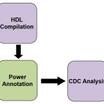
Figure 1. Power Aware CDC Flow
So, what is the solution?
In order to verify this type of design, you need to represent the design with the all of the domain information in place. The designer needs to know which power domain a signal belongs to, they want to know which clock domain it belongs to, and they want to know which reset domain it belongs to. That way they can make the decision as to whether there is a CDC problem or not. Because the power domain will impact the clock and reset domains, we want to present this information so that when the designer makes a decision of partitioning, they understand immediately the impacts on the other things in their design.
Designers now have a new flow available to help them get these tricky domain crossings right. Mentor’s Questa CDC solution supports a new concept in UPF 2.0 and UPF 2.1 called the power supply set(not to be confused with the power supply net). This is a power network grouping option that allows designers to define and test the power distribution network earlier in the project cycle before the power distribution network has been implemented. So you don’t need to know the physical implementation yet. Using the supply set, I can define the power domain at the RTL level early in the design cycle without knowing which voltage or power supply net it is actually connected to. So you can verify this regardless of how the supply net will be implemented.
The new power distribution network in UPF 2.1 is an example of the successive refinement methodology you’ve been talking about in your blogs, Ellie. In this context, the power network can be incrementally built over the duration of the project cycle by the different design project teams. The block and system designers can begin to verify the power management logic before the power distribution network has been implemented, then the final power management logic verification will occur later in the design flow when the physical designers add the power distribution network.
That’s very useful because when you are integrating multiple IP together, every IP can come with its own supply set. Now when you integrate, you can look at the supply set at the IP level and start finding a common ground to satisfy all the supply sets. And then you can design the supply net.
When we do the verification, we can now actually look at the supply set and figure out, by looking at the supply set, how many power domains you have in your design. Using the supply set information you can make sure the design can support those power domains later on. You use the supply set to verify whether your clock and reset trees were partitioned correctly. Once you have the tree information refined, you can run the CDC analysis using Questa CDC.
Our customers have already had success using our CDC solution in production. For example, AMD presented a Power Aware CDC (PA-CDC) verification paper at DAC in 2014. One of the things they uncovered was that control signals were not synchronized. They reported that complete PA-CDC checking at the RTL allowed them to find issues earlier in the design cycle and make turnaround times faster, and they used the PA-CDC flow to double check their generated UPF files against the RTL design.
Thank you, Ping, for giving us a quick insight into the effects of advanced low power management techniques on CDC design and verification. For those wanting to learn more, please check out the new whitepaper, Power Aware CDC Verification of Dynamic Frequency and Voltage Scaling (DVFS) Artifacts, which was presented at DVCon Europe 2015.
I’ll see you next year when we talk about what to look for in a low power debugging flow.