To pick up on my last post, I wanted to expand a bit on my duties and experiences back in 1979 in the 3″ Diffusion area of fab.
I am a morning person so I was usually at work between 6am – 7am. I would immediately go into fab to check on my engineering hold table and speak with the production operators to get a sense of the problems they were having. This helped me to plan my day. The average wafer lot size was 50 wfs/lot, not 25 wfs since the wafers were much smaller than they are today. Each lot on hold would have a completed engineering hold form that would detail why the lot was on hold. My engineering technician (a nice lady named Viola Brann) and I would then proceed to diagnose and disposition this material. This often required measuring oxide thicknesses and junction depths, and processing the lots through diffusion repair cycles to get them back into the production flow. We would later review the end-of-line parametric data on each lot to get feedback on the effectiveness of the repair cycle.
In stark contrast to the advanced metrology equipment of today, we had only very crude methods for assessing process performance. For example, to measure the thickness of silicon dioxide, we would take a Q Tip, dip the wooden end into a straight HF acid bath (with acid gloves on of course), and place one drop on the backside of the wafer to be measured. The HF would etch the oxide film very fast, leaving a colorful fringe pattern consisting of the colors of the rainbow. We would then estimate the oxide thickness looking up the last color present in the color chart table (reference: Semiconductor Technology Handbook – R.A Blanchard and O.D. Trapp) as shown below. If the surface oxide was blue in color and the fringe pattern showed one other blue cycle present, we would estimate the oxide thickness to be approximately 0.31um, or 3100A.
It didn’t take too long to be able to estimate the oxide thickness by just looking at the color. Of course the measurement accuracy (+/-150A) left something to be desired.
The technique used to measure the silicon dopant junction depths was just slightly more refined but extremely crude by today’s standards. Today we use SIMS analysis to measure dopant concentration into the silicon surface. In 1979, we used the lap and polish technique. Basically, we would cut off a small piece of the wafer using a diamond tipped scribe, mount it onto a cylindrical polishing block (using wax) that had a slightly sloped 4 degree bevel surface. We would then invert the sample and polish the mounted silicon using a diamond slurry until the 4 degree bevel had transferred to the silicon surface. Once the polishing was complete, a chemical stain was applied which served to stain the p-type regions (those containing high boron concentration) dark while leaving the n-type junctions light.
After the stain was applied, a cover glass was placed over the silicon sample and a sodium lamp (wavelength ~ 0.6um) was used to generate incident light creating a fringe pattern with each fringe separated by 0.3um. We would then inspect the beveled sample using a long working distance microscope through the cover glass and count the number of fringes from the silicon surface to the emitter-base (N-P) junction and then to the base-epi (P-N) junction. So, if we counted 7 fringes to the base-collector junction, that corresponded to a junction depth of 7 x 0.3um = 2.1um. If I remember correctly, most of our processes had junctions depths in the range of 0.9um to 4.2um+. The technique worked very well. One big drawback was the damage done to the product wafer in scribing off a piece for sectioning. You can imagine the silicon particles generated during that procedure.
Viola and I would often have to process the hold lots through furnace repair cycles ourselves as the operators were busy processing production material. Actually I greatly valued the direct “Hands-On” experience because it kept me very much in tune with all the duties that an operator had to handle. I developed a deep respect for their job and it kept me humble. One time, while sliding a load of wafers into the emitter diffusion furnace, I slipped and accidentally drove the quartz push rod into the first 10 wafers in the furnace, breaking all the wafers! Needless to say, the operators never let me forget that one.
I would come out of the fab at 9:00am for morning break in the cafeteria. We would sit at our usual table with our co-workers from the Photo area, Joan Denyer, Sheila Proctor, Rolf Dries, Alicia Eaton and Ron Gagne to name just a few. Over coffee, we would talk about almost anything. The workers in Photo were always blaming the workers in Diffusion for process problems and vice-versa….but it was all in good fun.
One last thing. The absolutely most valuable tool I have from my initial year at Fairchild is my own Semiconductor Technology Handbook (see photo below):
I first received this handbook during my initial training back in the summer of 1979 and still have it today. As you can tell it is well worn as I still use it on occasion today.
More to follow….

Low Power LTE for IoT: The Webinar from CEVA
Talking about “connected devices”, we specify any system from high-end smartphones to the simplest low-cost tag, as far as this system will be wirelessly connected. IoT are by definition connected systems, and represent a significant portion of connected devices. By 2020, ABI Research predicts that there will be more than 45 billion connected devices worldwide. More than half of these devices will incorporate multiple standards in the same device, such as Wi-Fi, 802.15.4g, GNSS and cellular, including the upcoming ultra- low data rate LTE MTC Cat-M.
Some application, such as wearable, will only require a battery life of a few days, but others such as asset trackers will demand a battery life of 5-10 years. For system designers, addressing wearable related challenges will be completely different than designing an asset tracker. As of today, some wearable devices are considered as fashionable gadget, the end user accepting to pay sometimes more than for a mainstream smartphone even if the battery life is only a day or so. The designer is free to define a complex architecture, supporting multiple wireless communication standards in the same device, as soon as the end product is feature-rich enough to attract the buyer. Final cost or power consumption are important parameters, but if the system is attractive enough to justify a buying act, neither high cost nor poor battery life will prevent to develop the system.
At the other side of the scope, if you define asset tracker system specification, you may end up to count every cent as you need to meet very stringent cost requirement and the battery life is expected to last several year instead of days. It’s clear that one wireless communication standard can’t fit the demand coming from so different applications. But how selecting the right wireless standard in respect with your system needs?
This webinar from CEVA’s experts will precisely address this question. Starting by an overview and market trends in connectivity for IoT and Machine to Machine (M2M), the webinar will introduce to the latest Low Data Rate LTE standards, including LTE Cat-1 and LTE Cat-0. There is a momentum behind LTE Cat-1 and LTE Cat-0 for IoT applications that don’t need the higher bandwidth rates delivered by the version of LTE (known as Cat-4) used by today’s smartphones. CAT-1 is a 3GPP-defined LTE specification that has a maximum downlink speed of 10Mbps, upload rate of 5Mbps, and is more cost- and power-efficient than Cat-4. CAT-0 will allow for even lower bandwidth (with a maximum throughput of 1Mbps) and more power-efficient LTE connectivity in the future.
CEVA’s expert will emphasize the importance of the processor architecture to efficiently enable multimode connectivity solutions. Finally, they will describe how implementing actual solutions for various IoT and M2M use cases using the latest communication DSP.
Who should attend? If you are a curious engineer or marketer, you certainly could attend. But you definitely should attend if you are communication and systems engineers targeting multimode applications requiring emerging cellular protocols such as LTE MTC Cat-1, Cat-0 or Cat-M, the Low Power Wide Area Network (LPWAN) standards such as Lora, SigFox and Ingenu, or any other IoT-related communication standards, including Wi-Fi 802.11n, PLC, 802.15.4g, ZigBee/Thread, GNSS, NB-IoT and Wi-Fi 802.11ah.
IoT Innovation Enters Public Infrastructure
I often hear about IoT being overhyped on what it needs and what it can actually provide. However, in my view, truly there seems to be a large potential in IoT enabled technologies and applications which we will see over upcoming years in the near future. It will gradually proliferate into various segments of our environment through automation and integration of devices with internet and semiconductor devices will be the driver.
Talking about the cost of IoT systems and expecting them to be cheaply available; think about the huge money spent on public infrastructure by the governments and public institutions around the world. Imagine how the use of IoT systems can save a significant portion of that public fund, yet make the public infrastructure more efficient, productive, safe, secure and easily manageable with little effort and effective use of resources.
The story has begun with Los Angeles being the world’s first city to have smart poles for street lighting that will serve dual purpose; smart lighting and smart data coverage with 4G LTE wireless technology. Ericsson has developed 4G LTE small cell technology that can be fitted on the light poles and can host mobile network operator equipment.
It’s a joint effort by Royal Philips (a global leader in lighting) and Ericsson. Royal Philipswill equip their LED light poles with fully integrated 4G LTE wireless technology from Ericsson and deploy them around the streets of LA. One can imagine how productive and efficient this collaborative technology will be. It will connect all light poles, reduce network tower clutter, provide better broadband connectivity and better network performance in dense urban localities.
Leveraging the street light poles for data traffic management will be a boon for IoT in smart cities where the volume of data is expected to grow multi-fold. The smart poles with 4G LTE will support increasing requirement of capacity to handle large data as well as efficient management of the data traffic without signal dropout.
On the other hand, the public lighting infrastructure is being infused with intelligence that can make the overall lighting system ‘smart’ and energy efficient. Also the real estate and infrastructure that’s already in place is now made smart to earn revenue by providing various network services.
The connected smart lighting system can be controlled remotely and managed very efficiently to save energy. The light levels can be adjusted according to the need in different streets from pole to pole. The lighting can be scheduled at times of the day, days of the week, and seasons and so on for different areas of the city. In fact, in the spirit of future IoT, the poles also can have sensors to detect traffic on the road and accordingly determine to keep the lights on or off.
The street lights in LA are already being controlled through a remote light management system. The Royal Philips CityTouch system connects each light point and uses mobile and cloud-based technologies to monitor and control street lights. The chip enabled light fixture in a smart pole can identify any fault in its light and report instantly to the control office through the connected system for the light to be repaired in time. Using this system uninterrupted and better lighting is provided at reduced maintenance cost and energy expense.
The system has a web based visualization tool that accurately monitors energy consumption and status of each light and reports the overall status in charts and diagrams. The report can also be used in planning the overall lighting system for the city. Here is a quick video of the CityTouch connect –
The CityTouch workflow is another web based asset management tool that provides complete visibility about the lighting assets and workflow for efficient decision making. It provides map based navigation to automate operations management. After reviewing appropriate level of details, fault reports can be created, work orders made, and distributed to maintenance crew for timely repair or installation. Here is a quick video on the CityTouch workflow system –
This is a great time to make our world smart. We are yet to see the unknown potential of IoT enabled systems in our overall ecosystem.
Pawan Kumar Fangaria
Founder & President at www.fangarias.com
Powering the IoT – Wishful Thinking versus Reality
There’s a lot of discussion these days on IoT applications, architectures, communication, security and more, all very good stuff, but little debate on how these devices will be powered. If you can plug them in, this maybe isn’t an issue (though we may need to think about increased demand on our overstrained power generation infrastructure). However, for mobile and remote applications, the question is commonly dismissed as something that can be resolved through energy-harvesting, without detailed investigation of how practical that option really is, at least from what I have read.
I too thought that energy harvesting was a really exciting direction, but was frustrated by many popular articles that, while starting from real research/applications, seem to point without support to wildly-extrapolated implications. So I did my own literature survey, with a bias to journal articles rather than popular articles wherever possible and what I found wasn’t quite so promising.
A quick summary:
· Inductive charging and wireless-beamed power are very practical but limited by heat generation and safety and of course by proximity to a wall-plug powered source
· Piezo- and thermo-electric charging are limited to order of uA/cm[SUP]2[/SUP]
· Biochemical charging can get to mA/ cm[SUP]2[/SUP] but the enzymes required for this method have to be replaced every couple of years
· Ambient wireless charging value is negligible unless very close to an antenna (if we could get this to a realistic charging level, I would worry about being cooked while I charge)
· Nuclear, surprisingly, is order of uA/cm[SUP]2[/SUP] or less apart from radio-thermal which is not considered safe for public use
· Biomechanical varies widely depending on the method used but suffers both from being a very intermittent source and potentially being tiring to use (you are the real power source)
· There are some scaled-up sources, such as piezo harvesting traffic pressure in roadways, building vibrations and vibration in railway tracks that can generate meaningful power (~100W for regenerative shock absorbers in cars and on tracks to ~10kW from skyscraper building dampers).
· One bright spot is photovoltaic (solar). Power density is still at the uA/cm[SUP]2[/SUP] level but we know how to scale up solar panels. A 10cm[SUP]2[/SUP] panel (a large watch face) could in principle power an LTE radio with a 1% duty-cycle. But of course solar is limited to outdoor applications.
None of these numbers is very exciting. Apart from solar, the problem seems to be that tapping new sources starts with a relatively small amount of practically and theoretically accessible energy which is then substantially reduced by unavoidable limits and inefficiencies in conversion. One way to offset this problem is through massive scale-up, but then you are limited to platforms like buildings and bridges. And even in those cases, the amount of energy that can be generated is dwarfed by the daily needs of the structure (a skyscraper for instance). I might wish the reality were different, but I suspect outside of the commercial successes we already know, this aspect of the green movement will have a rather short life. All of which may mean we’ll be stuck with the grid, batteries and proximity charging (inductive and beamed) for the foreseeable future.
I published my findings in a couple of LinkedIn blogs, the first on limitations to powering wearables and the second on limitations in locally-generated power (power generated close to the consumer of power, without connection to the grid). What I hope is different between my research and what appears in popular articles is that I tried to survey widely and I documented all my sources, so you can check what I found. I would be very happy to see supported counter-examples, because it really would be fantastic to find that there are practical local-scale harvesting technologies.
The link on limits to wearable power is HERE (the blog starts with power consumption in wearables; the generation part is in the second half of the blog). The link on limits to locally-generated power is HERE.
IEDM 2015 Blogs – Part 1 – Overview
The International Electron Devices Meeting (IEDM) is one of, if not the premier conference for semiconductor process technology. The 2015 meeting just finished up on Wednesday, December 9th.
This year’s meeting was held from Saturday, December 5[SUP]th[/SUP] through Wednesday, December 9[SUP]th[/SUP] in Washington DC. As a side note the conference has historically alternated years between Washington DC and San Francisco but after this year will be held exclusively in San Francisco. Basically with the so much of the semiconductor industry now located in the Far East attendance is better when the conference is in San Francisco.
I find the conference to be very helpful in terms of understanding the latest process technologies. Not only is the conference very good but there are a lot of side events held around it during lunch and the evenings.
Saturday
A series of six tutorials was held although I didn’t attend any of them.
Sunday
On Sunday there were two all day short course, one on CMOS for 5nm and beyond and the other on memory technology. I attended the memory technology seminar and I will blog about that in a subsequent blog.
Sunday night CEA-Leti and IMEC each held technology forums. I attended the IMEC forum and I will blog about that. I am also trying to set up a briefing from LETI on their recent work and if that comes about I will blog about that as well.
Monday
Monday opened the conference technical session with the plenary session. I will blog about Greg Yeric’s excellent address on Moore’s Law at 50 in a follow on blog.
At lunch on Monday I attended the press luncheon. General attendance for the conference this year is expected to be around 1,400 with 365 attendees for the tutorials and 505 attendees for the short courses. There were also two luncheons and they were expected to be sold out. Both David Lamers and myself asked about Platform CMOS papers and industrial participation. In general our impressions are that the conference has become more academic and less industrial practice oriented. The organizers felt that has been steady since 2005. They did agree that before 2005 there were more “platform” papers and they attributed that to consolidation. There was also a feeling that platform papers tended to be every other year now.
Monday afternoon I got a briefing from Global Foundries on their 22FDX technology and I will be blogging about that.
Micron and Intel presented their floating gate 3D NAND technology Monday afternoon and I will likely blog about that paper as well.
Tuesday
The conference continued on Tuesday with more technical papers. I am still organizing my thoughts on Tuesday’s papers but I will likely blog about what I saw.
Tuesday night I attended Coventor’s “the last half nanometer” panel discussion and I will blog about that.
Wednesday
The conference wrapped up Wednesday. There were a couple of excellent DRAM papers from Samsung and SK Hynix and I will blog about them plus possibly some other papers from Wednesday.
Wednesday at lunch I attended ASM’s luncheon where Dino Triyoso from Global Foundries presented. Unfortunately I was asked not to blog about that event.
Conclusion
IEDM 2015 was another excellent and informative conference. I will follow up this blog with approximately 8 or more blogs on what I saw.
3 flavors of TMR for FPGA protection
Back in the microprocessor stone age, government procurement agencies fell in love with the idea of radiation hardened parts that might survive catastrophic events. In those days, before rad-hard versions of PowerPC and SPARC arrived, there were few choices for processors in defense and space programs.
One of the first rad-hard microprocessors was the Performance Semiconductor PACE P1750A, a product line since acquired by Pyramid Semiconductor. It was born in the Reagan-era “Star Wars” boom, where total ionizing dose (TID) and low power consumption were the first two requirements. Thank goodness, our project using the PACE P1750A never got past system design and lab prototyping, because I don’t think we fully appreciated what we were up against in creating a totally rad-hard, space-ready system.
What the semiconductor industry has learned about rad-hard and rad-tolerant design since fills volumes of books and is still developing. Geometries have shrunk, worsening the chance of a disruption from radiation. Processes have improved with technology such as silicon on insulator (SOI). Software content in all projects has swelled, justifying investments in creating rad-hard processors delivering a high level of confidence at a high level of cost.
Rad-hard ASICs, however, are another matter. While the technology exists, the volumes around a custom design usually do not. Fortunately, FPGA vendors and some defense firms licensing technology have stepped in with rad-hard parts targeting space-based projects.
Space is not the only place radiation exists. Many applications, including industrial, medical, and automotive, are subject to single event upset (SEU). To provide adequate levels of safety-critical operation without the expense of full rad-hard FPGAs, designers are turning more and more to SEU-tolerant approaches in FPGA logic synthesis. These same approaches are even applicable in full rad-hard FPGAs, as various FPGA technologies present different susceptibility and need additional mitigation techniques in some areas.
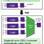
The cornerstone of SEU mitigation is triple modular redundancy, or TMR. This is the classic voting scheme, where circuitry is replicated three times and combined into a majority voter. In theory, if an SEU occurs in one block, the other two provide correct results. TMR schemes can detect and correct single-bit errors.
Dialing in TMR by hand in a complex FPGA-based design could take forever, take a lot of area on the chip, and potentially mess up timing. Understanding the tradeoff between safety, area, and timing can make or break a project. Synopsys has spent significant amounts of research on its Synplify Premier tool, studying popular FPGA architectures and mitigation approaches, to automate the insertion of TMR during synthesis.
For instance, there are actually three flavors of TMR. Registers can be protected with local TMR (LTMR), a simple replication. However, researchers are finding SRAM-based FPGAs in space-qualified applications are still susceptible to upset using LTMR – geometries are small enough and events rapid enough that radiation strikes two or even all three blocks.
To protect I/O and logic and provide more hardening for space-based designs, distributed TMR (DTMR) physically separates the triplicated circuitry on the chip. Block TMR (BTMR) takes the approach a step further with physical separation and clock synchronization, and can be used with indivisible or encrypted IP blocks.
Synplify Premier handles all three of these TMR types and more mitigation techniques, with automated FPGA-aware synthesis techniques supporting all popular devices. Synopsys application engineer Sharath Duraiswami dives into the details in an archived webinar:
Building Highly Reliable FPGA Designs for Applications Needing Functional Safety
One idea Sharath discusses is “partial DTMR”, where voters around flushable dual flip-flops are optimized to save area when possible. He also shows how the physical separation works, along with Synplify mitigation techniques for each type of functional block in an FPGA including duplicate with compare (DWC), Hamming-3 encoding, and safe case FSM. One example even shows use of a Xilinx Zynq-7000 SoC using DWC techniques for error control.
The webinar tips will be helpful for designers working with full rad-hard FPGAs or trying to harden safety-critical applications, whether working with Altera, Lattice, Microsemi, Xilinx, or other parts. It’s evident just how much work Synopsys has put into Synplify Premier to automate synthesis for a wide variety of scenarios, far beyond just blasting away with logic triplication. I like this presentation because it isn’t tied to just one FPGA architecture or vendor – each has its merits and limitations in safety-critical design that engineers need to be aware of.
The Mobility Imperative and the Untethered Consumer
Consumers want to be able to go where they want, when they want. They want televisions to be seamlessly synchronized with tablets, phones, laptops, and automobiles. They want all their communication, information, and entertainment to be available immediately, with high resolution, all the time. Recently the automobile industry has caught on to this trend and has begun to show its vision of the future for the fully mobile lifestyle.
They also do not want to worry about running out of battery life – no more looking for an outlet at the airport. This untethered life is the Mobility Imperative and it is driving innovation in consumer products, which in turn, is pushing the limits of silicon-based semiconductor technology.
As silicon power transistors (MOSFETs) run out of gas, gallium nitride transistors are the next generation semiconductor devices in the world of power conversion and data transmission. Enhancement-mode gallium nitride transistors (eGaN[SUP]®[/SUP] FETs) from Efficient Power Conversion Corporation (EPC) have been in production for over five years. These devices are smaller in size, superior in performance, and lower in cost when compared with their aging silicon ancestor, the power MOSFET. GaN’s high-speed capability, coupled with lower production costs and smaller size, makes this technology ideal for accomplishing the Mobility Imperative.
Increasing Wireless Bandwidth – Increased Data Transmission, Increased Battery Life
Envelope tracking is a power supply technique for improving the energy efficiency of Radio Frequency Power Amplifiers by precisely tracking the power demand, as compared to today’s fixed-power systems. In cell phones use of envelope tracking means longer talk time, and in base stations it means smaller, less expensive amplifiers that consume far less energy and are less expensive to operate.
As our demand for wireless data grows, the value provided by envelope tracking increases dramatically. More transmitters alone cannot solve the problem; rather, more data transmission bandwidth per power amplifier is required. As the data transmission bandwidth increases, the efficiency of the transmitter’s power amplifier sharply declines unless the system adopts envelope-tracking methods.
Gallium nitride is being seen as an enabling technology for both envelope tracking converters and wide bandwidth RF Power Amplifier designs. The ultra-fast switching capabilities of eGaN FETs enable the high frequency, multi-phase buck converters used in envelope tracking power systems.
Figure 2: An example of an envelope tracking system using eGaN FETs. eGaN FETs are the tiny blue rectangles on the circuit board. (Photo courtesy of NewEdge Signal Solutions.)
Wireless Power Transfer Cuts the Cord…No Need to “find an outlet!”
Since Nikola Tesla first experimented with wireless power during the early years of the 20[SUP]th[/SUP] century, there has been a quest to “cut the cord” of electrical power – and go wireless! Now, more than 100 years later, the technological capability to achieve Telsa’s vision is a reality.
Highly resonant wireless power transfer, based on the generation of magnetic fields, has proven to be a viable path. Magnetic fields offer the necessary requisites for implementing wireless power – ease of use, robustness and, most importantly, it is considered safe. Applications for wireless power are endless, from charging cell phones and computers, to powering systems in hazardous environments and implantable medical devices.
With the explosion in the variety and number of mobile devices, wireless power transfer offers the convenience of charging batteries without the annoyance of cumbersome cables and the inconvenience of looking for outlets to “plug in.” Figure 3 is an illustration of what the home of the future might look like with all electrical appliances powered without power cords.
Over the past several years, three standards for wireless power transmission have emerged. These standards, put forth by industry consortia include the Wireless Power Consortium’s Qi, the Power Matters Alliance and the AirFuel Alliance standard, also known as Rezence[SUP]®[/SUP]. Only the technical approach embodied in the Rezence standard allows multiple gadgets to simultaneously charge from a single transmitter at a significant distance.
Figure 3: In the future electrical power cords may become obsolete as illustrated in this vision of the home of the future
The Rezence[SUP]®[/SUP] standard for wireless power transmission is about to see rapid adoption in mobile phone and tablet charging applications. For example, several automotive manufacturers are planning to embed wireless charging systems in the center console of their vehicles so the smartphone, as well as other mobile devices, can remain charged despite intense and continuous usage while the automobile is in operation. Given that the Rezence standard requires a high speed, 6.78 MHz, frequency for power transmission, eGaN FETs are the heavy favorite for adoption over the slower and less efficient silicon power MOSFET.
Figure 4: Wireless power transfer will be used in automobiles to keep smartphones charged despite continuous usage as part of the infotainment system. (Photo courtesy of Gill Electronics.)
Wireless charging for electric vehicles is also becoming more available as electrically powered cars become more prolific. Although there is no universal standard yet, loosely coupled magnetic energy transfer, similar to the method used in the Rezence standard, is common to all implementations. This is due to its ability to transfer power without precise alignment of transmitter and receiver units. eGaN FETs are certainly a good candidate technology for this application.
Automotive Sensing and Autonomous Control – Collision Avoidance or “Relax and Enjoy the Ride”
For safety reasons, it is critical that a car know what is around it at all times. This becomes even more essential as the car evolves into a self-driving machine. Further, the higher the speed of the vehicle and the more complex the surroundings, the faster the environmental sensing system needs to be, and the more precisely it needs to interpret the distance to a potential collision.
Today automotive manufacturers use a variety of sensors in these functions, including Light Distancing and Ranging (LiDAR) sensors that have only recently begun to emerge in automotive sensing autonomous driving applications.
Summary
In conclusion, a “Mobility Imperative” is upon us…the modern consumer is demanding that:
· they do not want the range anxiety caused by the worry about running out of battery life and having to “find an outlet.”
· all their information and entertainment be available all the time via their smartphone …all in high resolution and all “right now”
Gallium nitride is the fundamental technology bringing the “Mobile Imperative” to reality since it provides:
· increased switching speed leading to higher resolution and less power consumption.
· smaller size, thus enabling product miniaturization and weight reduction.
· low product costs, thus stretching the consumer dollar farther.
Consumers want to be able to go “mobile” wherever and whenever they want…this is today’s Mobile Imperative and it is driving innovation throughout consumer electronics.
The current semiconductor technology, silicon power transistors (MOSFETs), has reached its performance limits; fortunately, gallium nitride transistors with their high-speed capability coupled with lower production costs and smaller size, has come of age. It is GaN technology that will make Tesla’s vision come to fruition…and make it possible for us to achieve the Mobility Imperative.
Does Managing Tools as if they are IP Make Sense?
Years ago I thought that chip design companies would embrace the latest technology and be eager to adopt new tools. What I learned was that the people implementing and managing design projects were taking a lot of risks with almost every aspect of their projects. What they most wanted is to minimize risk from the design process – especially from design tool changes.
The reluctance to change goes much deeper. In the middle of a project a design team would never be willing to change tools, or even tool versions. Even minor updates from vendors can have subtle algorithmic changes that affect results. Beyond the obvious possibility of an outright bug, there can be variations in results that can affect every downstream step. This is true for implementation and sign off tools.
Chip companies spend significant resources on correlation and validation of tools. In some cases, known bugs in software are compensated for and if a tool vendor were to suddenly fixed the bug it could break the flow. Pretty much the only reason a design team will change any tool or tool version is to fix a show-stopper issue.
Now, think about how many tools there are in the the typical design flow. Each one of these tools has configuration files, rule decks, libraries or stack-up information, and command scripts that drive the tool. If anything changes it can ripple downstream.
Broadening our scope, the same reasoning applies to all the PDK data. PDK’s contain thousands of files. Stability of the PDK through a project is essential. Nevertheless, some project cannot avoid PDK changes because the foundry is refining the process, and those changes need to be adopted across the entire project prior to tape-out.
Presently, large team projects usually already use data management for the design data, maybe even rule files. As we can see from the discussion above the same kind of management that is used for design data could be beneficial when applied to the tools in the flow.
Methodics Inc., a data management company for EDA, has just written about how they support complete management of the design environment using their software. They point out that large teams spread out in locations around the world need to have consistent and well managed tool environments. Treating the design environment as if it were IP allows a systematic way of managing all the tools in the flow.
Using a variety of techniques, it is possible to make setting up the user environment efficient and fast. One frequent concern is whether making multiple copies of all the tool installations is necessary. Methodics gives customers the choice of instantiating the files or using soft links to save space and copying time. Another important consideration in their solution makes it possible to handle user specific customization, while ensuring before the final project release that known versions of all the tools are used in the final tape out flow. It is also possible to switch tool release versions and keep old tool environments available in case there is a need to roll back a tool update.
The Methodics white paper goes into more detail describing the different ways their solution can be deployed. But there is no question that managing the software used for a design project is just as important as managing the design data itself.
5 Verification Challenges of IoT Solved by Emulation

Software-centric Emulation environment takes the forefront in modern SoC verification. As more and more devices are IoT enabled, the SoCs have to make special provisions to factor many things including communication, power usage, and network switching, and so on. Also, the demand for an SoC (specifically for smartphone which is pivotal for IoT) to handle multiple functions pertaining to audio, video, data, mobile etc. increases the size and complexity of the SoC significantly. Considering the three connection points for IoT; endpoint, gateway and cloud, the complexities of chipsets increase in that order. An SoC for cloud (data center) application, or even for gateway application has to handle what we call “Big Data” coming from multiple sensors from all connected devices through the system.
Traditional verification methods such as simulation with testbench approach or even traditional in-circuit emulation (ICE) are not sufficient for verifying such SoCs. There is a need for a more robust, software-based, virtual emulation solution that is scalable, flexible with job sharing and remote access facility for multiple teams to work at a time, easy-to-use, and reliable without much cabling in the system.
By now we are aware of Mentor’sVeloce emulation system coming out of the closet for remote teams to run their live applications on it. During this year’s DAC, Mentor also announced Veloce’s integration with ANSYS’PowerArtist for advanced real-time power analysis early in the design cycle.
Let’s review Veloce in the context of an emulation data center and see how it addresses the key verification challenges of an IoT-centric SoC or any other mobile SoC for that matter.
Veloce VirtuaLAB is a software-based virtual emulation data center with Enterprise Server capability that requires only the emulator and workstations to execute the software versions of the protocol models. The emulator has a single operating system, Veloce OS for all applications (internal or third party) to run on it. The Enterprise Server optimizes resource utilization and job sharing through LSF software.
Multiple users from remote sites across the world can concurrently access this emulation system for multiple projects from their desktops. The VirtuaLAB models can be easily reconfigured by simply changing their compile parameters as required. Let’s see how this system addresses the five key challenges –
Protocol Solutions – Chips are accommodating increasing number of protocols. Veloce offers software-based solutions including host/peripheral models, protocol exerciser/analyzers, and software debug for multiple market segments such as mobile, networking, multimedia, and storage interconnect. These are mostly IP-based. It’s expected that the solution be extended for other popular IoT frameworks as well.
Larger Designs – Veloce provides a scalable platform for increasing sizes of SoCs – Quattro for up to 256 million gates / system and up to 16 users; Maximus for up to 1 billion gates and up to 64 users; Double Maximus for up to 2 billion gates and up to 128 users.
Lower Power – Veloce can boot the OS and run billions of cycles to fully exercise live software applications running on the target hardware. As said above, third party power analysis tools such as PowerArtist can be integrated with Veloce to get accurate power analysis numbers for real applications early in the design flow. This is a unique capability of Veloce.
Debugging large software content – The software in IoT context can be varied for edge, gateway, and cloud. Veloce provides a virtual environment where different applications can run on the same Veloce OS. Virtual Probes which provide virtual connection with the software debugger are used for live interactive debugging.
When the emulator is off, Veloce Codelink supports offline and re-playable debugging for multiple, concurrent users. Multiple databases are generated by the emulator which can be used offline for debugging, thus freeing up the emulator for other tasks and users.
Network Switch and Router Ports – In IoT applications an SoC can have thousands of ports making it impossible to provide connections in hardware test environment. Veloce VirtuaLAB provides most of the test environment into software where the emulator is connected to the user environment on a workstation through one or more software connections that enable the user to interact with the DUT running in the emulator. As an example, for Ethernet, there is Ethernet Packet Generator and Monitor (EPGM) application that runs on the workstation to generate virtual Ethernet traffic and provide visibility, analysis, and user control of the traffic.
The Veloce virtual emulation data center is a step in the right direction to support massive amount of verification needed to design the products and networks for IoT world. It provides better reliability, scale of operation with multi-user environment and remote access, lower cost of operation, and better quality with higher debug visibility in a software-based environment.
More details can be found in a whitepaper written by Richard Pugh on the Mentor Graphics website HERE.
Also read: Power Analysis Needs Shift in Methodology
Pawan Kumar Fangaria
Founder & President at www.fangarias.com
Cadence Enters the RTL Power Estimation Game

At the Cadence front-end summit last week, Jay Roy presented the Cadence Joules solution for RTL (and gate-level) power estimation. Jay is ex-Apache, so knows his way around RTL power estimation which should make Joules a product to watch. Joules connects very natively to Palladium for power characterization for realistic software loads, which I’ll cover in a separate blog. Here I want to focus on Joules as a characterization competitor to Apache/Ansys, Atrenta/Synopsys and other products.
Jay’s claim, and I think he’s right today, is that Joules has all the pieces to get high accuracy for RTL power estimation. They have Genus for synthesis and Innovus for implementation so they can do (somewhat) production quality fast estimations straight from RTL and know they are (somewhat) going to correlate with the real implementation, and therefore they can get power estimates from RTL simulations which will correlate within ~15% of gate-level estimation. Jay showed a table of comparison which indeed support this assertion.
You may notice I am (somewhat) hedging my support for the attainable level of accuracy. I also know a little about this domain and some of the challenges in RTL estimation. Part of the problem is indeed in using the same tools for fast physical synthesis as you use for production implementation. But that’s not all of the problem. Fast physical synthesis is fast because it cuts corners and that can lead to correlation problems between RTL and gate-level estimates, even if you use the same physical synthesis tools you use for production.
It seems obvious that the way to understand this problem should be a detailed analysis of sources of miscorrelation between RTL and gate-level estimates. But I have yet to see such an analysis from any provider and that’s a problem because it leads to unscientific trial and error approaches to improving correlation, with no deep understanding. Scientific approaches (you know, start with a hypothesis, test against data) would provide a credible basis for knowing how to repeatably improve correlation or, just as important, knowing that perhaps 15% is as low as you can go and you cannot repeatably improve on that. This would be a lot of work, but whoever does this first will be able to claim the laurels of true expertise in this domain.
I don’t think it is necessary to test every conceivable design – that would not be a scientific approach. Useful hypotheses are simple – I’ll offer a couple to get the ball rolling. First, I believe the harder you push performance, the worse the correlation will become. The harder you push, the more buffers have to be upsized; also there are implications for routing in the presence of factors not considered in fast estimation (DFT, detailed routing, signal integrity, …), leading to yet more buffer upsizing, further impacting power. A related but not identical hypothesis is that accuracy will negatively correlate with the number of near-critical paths. As you get into implementation, some of these will become critical, requiring (probably) buffer upsizing; the more of these you have, the more implemented circuit power will deviate from initial estimates. Cadence has a running start with a fully integrated solution which should minimize known systematic sources of error from the estimation tool – they could lead the field with a detailed correlation analysis.
None of this is intended to diminish the role Joules can play today. As far as I know today they have the only full in-house flow for estimation based on implementation class physical synthesis, so they are likely to be best in-class for estimation until Synopsys inevitably releases something similar. And then they will both have a significant edge in accuracy over Apache and Calypto for the foreseeable future.
To learn more about Joules, click HERE.