You are currently viewing SemiWiki as a guest which gives you limited access to the site. To view blog comments and experience other SemiWiki features you must be a registered member. Registration is fast, simple, and absolutely free so please, join our community today!
The Future Horizons Industry Update Webinar, presented today by Malcolm Penn, provides a comprehensive analysis of the semiconductor industry’s current state and future trajectory. Founded in 1989, Future Horizons leverages over 300 man-years of experience, emphasizing impartial insights from facts (e.g., IMF economy data, WSTS units/ASPs, SEMI capacity), sentiment (hype vs. reality), and decades of expertise. The agenda covers industry updates, outlooks on economy, unit demand, capacity, and ASPs, market forecasts for 2025-2026, key takeaways, and Q&A.
Malcolm opens by highlighting “truly extraordinary times,” driven by Trump 2.0’s “America First” agenda, which abandons free trade norms, raises tariffs to 1930s levels, and pivots to national interests. Geopolitical tensions—Netanyahu’s Gaza actions, Putin’s Ukraine aggression, Xi’s Taiwan threats—and China’s rise as a superpower challenge U.S. dominance, shattering post-WWII peace.
The market outlook is mixed: 1H-2025 growth relies on ASPs from the AI data center boom, masking non-AI weaknesses, excess CAPEX, and bloated inventories. Doubts emerge on AI’s ROI amid “insane” spending, with YoY revenue plateauing and a fragile U.S. economy. For 2H-2025, expect more of the same plus worsening economics, urging preparation for an AI “hangover” in a head (fundamentals) vs. heart (frenzy) battle.
Framing the analysis around the “Four Horsemen of the Semiconductor Apocalypse”:
Economy: Precariously unclear, with “tenuous resilience amid persistent uncertainty” (IMF July 2025). U.S. defies gloom, but EU/China stagnate; Trump shocks absorbed but risks linger. U.S. cost-of-living fears (70% worry income lags inflation) and Fed’s dual mandate conundrum (employment vs. prices) add pressure, with a September 17 rate cut a “dead certainty” but damned either way.
Unit Shipments: Yet to recover fully; July at 7.6b/week, 8% below peak, with unmeasured excess inventory choking supply chains (20b repaid of January’s 58b excess). Real recovery awaits unit growth resumption.
Capacity: CapEx stubbornly high at ~15% of SC sales vs. 11% trend, abnormal post-2022 crash. China is the culprit, accelerating to 34% global share (decoupling/tariffs-driven), 3x justifiable levels, focusing on non-leading edge but advancing (e.g., Huawei/SMIC 5/7nm). Domestic WFE vendors rise, closing markets; turning CapEx to capacity proves challenging (US$50-100b lost). India now ramps up ambitiously.
ASPs: Strong recovery from June 2022 crash ($1.11 to $1.85 peak), but plateauing/oscillating since December 2023. All sectors retreat except logic (TSMC’s SoC pseudo-monopoly holding prices). Long-term trend reverts to $1 (Moore’s Second Law), with disruptions temporary.
Forecasts: 2025 at +16% ($731.6b, range 15-17%), ASP-driven with early recovery in discretes/opto/analog; 2026 at +12% ($813.1b, range 6-18%), assuming no AI slowdown, stable geopolitics/economy, and unit rebound. Risks include AI crash, China dumping, overcapacity on mature nodes.
Bottom line: Technology roadmap to 2039 (GAA transition challenging, four-horse race: TSMC N2, Intel 18A, Samsung SF2, Rapidus 2nm). Power semis favor silicon over SiC/GaN/diamond; Makimoto’s Wave holds through 2037 (chiplets next). Packaging evolves from begrudging to enabling (ASATs vs. foundries). Next disruption: quantum computing, not AI (just improved tools). AI data center “madness” (e.g., 10GW plants, underwater/floating) and smart glasses echo 1970s watch disasters—ego over wisdom, fruition decades away. Chip drivers remain Moore’s Law, legislation, A/D conversion, geographic shifts—entertaining, drudgery-removing, enabling impossibles.
Malcolm also warns of structural risks (excess capacity, low utilization, economic tilts to bear), urging caution amid AI hype. Promotes monthly reports for tracking fundamentals., The next webinar January 20, 2026 which will be a must see round-up of 2025.
Digital design engineers have used DFT automation technologies like scan and ATPG for decades now, however, analog blocks embedded within SoCs have historically required that a test engineer write tests that require specialized expertise and that can take man-months to debug. Siemens has a long history in the DFT field, SPICE circuit simulation and AMS simulation, so it was a natural fit for them to announce analog component testing as part of a new product dubbed Tessent AnalogTest. I had a video call with Etienne Racine, Product Manager, Tessent to understand what’s new.
Testing analog components inside an SoC drives up the test costs, so there’s impetus to reduce this time through automation techniques. Scan for digital has now been extended into the analog realm. There’s an that talks about a novel DFT and ATPG technique that has minimal area and performance impact, and Tessent AnalogTest uses it as part of its technology.
Using such scan-based analog tests reduces defect simulation times from days to minutes and brings to analog very similar benefits as what digital scan and ATPG provided to digital designs several decades ago. Leveraging evolutive standards thus becomes important for broad adoption and EDA industry support.
IEEE P2427 is both a working group and draft standard that gives a standardized approach for analog defect modeling and coverage in Analog Mixed-Signal (AMS) devices, where the defect universe contains all likely defects, and also defines detectable defect coverage. The test idea is to inject a defect in the netlist, run a SPICE circuit simulation and then measure the effects to see whether the resulting fault is detected.
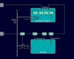
Users of Tessent AnalogTest can also use the IJTAG framework to enable portable and retargetable AMS function tests, defined in the IEEE P1687.2 standard. There’s a learning curve with the Instrument Connectivity Language (ICL) and Procedural Description Language (PDL) to describe the analog test access, instruments and analog test mechanisms. The automation helps users to create those files when they don’t already exist.
Figure 1: Example of a digital IJTAG network used to access an analog block during tests.
Test engineers write PDL for the AMS block, like force 2.5V on this pin, then measure the current on another pin. Tessent AnalogTest reads the PDL file, then creates a simulation test bench automatically. The Siemens tool also reads in the SPICE netlist for the AMS blocks, runs the SPICE simulator to detect injected defects, then reports coverage achieved. Two Siemens simulators are supported for analog defect/fault simulation and detection, AFS or Symphony.
This new approach with Tessent AnalogTest combining digital scan-based tests and analog IJTAG measurements improves AMS test coverage plus reduces test development and application times. When silicon arrives, your team can optimize defect coverage or yield, eventually extending this to automated defect analysis. Safety critical applications that use ISO 26262 functional safety metrics will benefit from this approach with a consistent, simulated, automated test description.
Learning and using the high-level PDL language to describe intended test sequences is a big time saver, freeing up engineering resources. IJTAG is well understood by test teams, so expanding that to include analog blocks is an easy process. The Tessent AnalogTest tool automates the creation of DFT circuitry along with test patterns to test most analog circuits in under 1ms on digital-only testers. Even the test times get reduced 10X-100X while providing similar defect coverage to specification tests.
Structural test waveforms, multiple outputs tested concurrently
AMS designs now have new automation technology to dramatically improve analog test development and reach coverage goals, while being connected with IJTAG scan chains and an analog test bus. Siemens has introduced something not seen before, so it’s exciting times. Following the IEEE standards P2427 and P1687.2 ensures that this technology will be supported by the EDA industry going forward.
MediaTek’s first chipset using 2nm technology expected in late 2026
MediaTek, a global leader in fabless semiconductor design, has announced a groundbreaking achievement in its partnership with TSMC. The company has successfully developed a flagship system-on-chip (SoC) utilizing TSMC’s cutting-edge 2nm process technology, with volume production slated for late 2026. This milestone reinforces the long-standing collaboration between MediaTek and TSMC, which has consistently delivered high-performance, power-efficient chipsets for applications spanning flagship mobile devices, computing, automotive, data centers, and more.
TSMC’s 2nm process technology introduces a nanosheet transistor structure, a significant leap forward in semiconductor design. This innovative architecture enables substantial improvements in both performance and power efficiency, setting a new standard for advanced chipsets. MediaTek’s first 2nm-based chipset, expected to debut in late 2026, will leverage these advancements to deliver unparalleled capabilities across a wide range of devices and industries.
Compared to TSMC’s current-generation N3E process, the N2P technology offers remarkable enhancements: up to an 18 percent increase in performance at the same power level, approximately 36 percent reduction in power consumption at equivalent speeds, and a 1.2x increase in logic density. These improvements translate into faster, more energy-efficient chips that can handle the increasing demands of modern applications, from AI-driven computing to high-performance mobile devices and energy-conscious automotive systems.
“MediaTek’s innovations powered by TSMC’s 2nm technology underscores our industry leadership, as we continue to push forward with the most advanced semiconductor process technologies available for a variety of devices and applications,” said Joe Chen, President of MediaTek. “Our long history of close collaboration with TSMC has led to incredible advancements in solutions for our global customers, offering the highest performance and power efficiency from the edge to the cloud.”
Dr. Kevin Zhang, Senior Vice President of Business Development and Global Sales and Deputy Co-COO of TSMC, echoed this sentiment: “TSMC’s 2nm technology represents a significant step forward into the nanosheet era, demonstrating our relentless dedication to fulfilling our customers’ needs – tuning and improving our technologies to deliver energy-efficient computing capability. Our ongoing collaboration with MediaTek focuses on maximizing enhanced performance and power capabilities across a wide range of applications.”
This development marks a pivotal moment in the semiconductor industry, as MediaTek and TSMC continue to drive innovation in chip design and manufacturing. The adoption of nanosheet transistors in the 2nm process enables greater scalability and efficiency, addressing the growing complexity of modern devices. From smartphones and AI-powered PCs to smart homes, high-performance computing, and AI data centers, MediaTek’s 2nm chipset is poised to redefine performance standards while prioritizing energy efficiency.
MediaTek’s commitment to advancing transformative technologies such as AI, 5G/6G, and Wi-Fi 7/Wi-Fi 8 positions the company at the forefront of the industry. Powering over 2 billion connected devices annually, MediaTek’s solutions are integral to creating a smarter, more connected world. As a trusted partner to leading global brands, the company continues to innovate, ensuring that its high-performance, power-efficient products meet the evolving needs of consumers and businesses alike.
The successful tape-out of MediaTek’s 2nm chipset is a testament to the strength of its partnership with TSMC and its dedication to pushing technological boundaries. By leveraging TSMC’s state-of-the-art 2nm process, MediaTek is well-positioned to deliver next-generation solutions that enhance everyday life and drive the future of connectivity and artificial intelligence.
About MediaTek
MediaTek is a global leader in fabless semiconductor design, providing innovative solutions from edge to cloud. Powering over 2 billion connected devices annually, MediaTek drives advancements in AI, 5G/6G, and Wi-Fi 7/Wi-Fi 8, enabling devices from smartphones and AI PCs to automotive and data centers. Committed to a smarter, more connected world, MediaTek ensures access to world-class technology for all. Visit www.mediatek.com for more information.
In the rapidly evolving landscape of semiconductor manufacturing, the demand for processors that handle increasing workloads while maintaining power efficiency and compact form factors has never been higher. Intel’s Foveros 2.5D packaging technology emerges as a pivotal innovation, enabling denser die integration and enhanced functionality without substantially expanding the physical footprint of chip packages. Introduced in 2019, Foveros 2.5D represents an advanced die-stacking process that assembles multiple chiplets (small specialized silicon dies) into a cohesive unit. This approach addresses the limitations of traditional packaging by layering active dies, such as logic, memory, or FPGAs, atop a passive base die equipped with through-silicon vias (TSVs). The base die, often called a silicon interposer, facilitates seamless interconnectivity, marking a shift from monolithic chip designs to heterogeneous, modular systems.
At the core of Foveros 2.5D is its face-to-face chip-on-chip bonding mechanism, achieved through an ultra-fine microbump pitch of 36 micrometers. This precision bonding minimizes wire parasitics—undesirable electrical properties like resistance, capacitance, and inductance that degrade performance due to interconnect layouts. By reducing these parasitics, Foveros 2.5D ensures higher interconnect density, which is crucial for high-performance applications in data centers, AI accelerators, and edge computing. Furthermore, the technology allows designers to combine advanced process nodes for cutting-edge components with mature nodes for cost-effective, proven IP blocks. This hybrid strategy not only optimizes yields but also lowers manufacturing expenses, as smaller specialized dies on advanced nodes can be paired with reusable elements on established processes.
The benefits of Foveros 2.5D extend beyond density and cost. By stacking components vertically rather than spreading them horizontally, it significantly reduces signal travel distances, thereby lowering latency and boosting overall system performance. This vertical integration also enables more compact designs, ideal for space-constrained devices like mobile processors and embedded systems. When paired with Intel’s Embedded Multi-die Interconnect Bridge (EMIB), Foveros evolves into EMIB 3.5D, expanding reticle limits and supporting even more intricate multi-die configurations. This synergy allows for the connection of passive dies, further enhancing scalability for complex chip architectures.
Intel Foundry offers a versatile portfolio of Foveros 2.5D variants to cater to diverse needs. Foveros-S 2.5D employs a silicon interposer to position multiple chips side-by-side, delivering superior performance and power efficiency over conventional methods. In contrast, Foveros-R 2.5D prioritizes cost optimization and interconnect density by eliminating the interposer and utilizing fanout with up to three redistribution layers, enabling flexible heterogeneous systems. For applications requiring multiple base die chiplets, Foveros-B 2.5D integrates active and passive silicon bridges with RDLs, paving the way for future enhancements like cache disaggregation, integrated voltage regulators (IVRs), or metal-insulator-metal capacitors. All these configurations align with the Universal Chiplet Interconnect Express (UCIe) specification, an open industry standard that Intel helped pioneer. UCIe facilitates high-density integration of chiplets from various vendors, promoting interoperability, energy efficiency, and bandwidth gains through asynchronous and synchronous communication.
The evolution of Intel’s packaging technologies—from wire-bond and flip-chip methods to advanced solutions like Foveros—underscores a paradigm shift toward “systems of chips.” This disaggregated approach, championed by Intel Foundry’s Advanced System Assembly & Test, supports full-stack solutions that accelerate time-to-market for demanding use cases. With geographically diverse manufacturing capacity and ecosystem partners for system technology co-optimization, Intel is positioning itself as a leader in the transition from system-on-chip to multi-chiplet ecosystems.
Bottom line: Foveros 2.5D exemplifies how innovative packaging can unlock new frontiers in semiconductor performance, efficiency, and scalability. By enabling heterogeneous chiplet integration, it not only meets current computational demands but also anticipates future challenges in AI and high-performance computing. As Intel continues to drive standards like UCIe, the technology promises to democratize advanced silicon design, fostering collaboration across the industry and ensuring that complex, power-efficient systems become the norm rather than the exception.
While stochastic defects link yield with the practical resolution of EUV lithography resulting from its quantum nature [1], very low yields of EUV processes are more readily linked to the use of EUV masks without pellicles. Pellicles are thin film membrane covers on masks (regardless of wavelength: EUV and DUV and i-line) used to protect from particles landing on the patterns on the mask. Particles could land on the pellicle, but they would not print because they would be so out of focus. Without pellicles, yield can drop significantly just from having a few particles land on the mask [2].
Surprisingly, it has been reported recently that EUV users generally do not use pellicles [3,4]. The key reason is that pellicles can be damaged or even ruptured due to EUV light exposure [5]. TSMC also reported in 2023 that its EUV pellicle infrastructure was just completed, but still not yet in production [6]. They also noted that “with the increase in scanner power to 400W, a pellicle lifetime challenge has been observed” [6]. Moreover, it has been reported this year that TSMC was reluctant to use EUV pellicles since they need to be replaced every 3–4 days, at a high cost of over $10000 each [4].
Without the use of pellicles, it has been necessary to periodically check if particles had attached to the mask in the pattern area [7]. Note that increased inspection frequency means fewer output wafers per month. This leads to a tradeoff between inspection cost and yield risk (Figure 1).
Figure 1. A lower inspection frequency can keep costs low but increases the risk of letting a dirty mask print more wafers. The risk is reduced with increasing inspection frequency, which also increases costs.
The struggle for yield without pellicles is in line with continuing reports of yields less than 70% [8,9]. Nevertheless, even this year, Samsung reported ongoing concerns with EUV pellicle lifetimes, even with more promising candidate materials [10]. EUV users concerned about yield will need to continue to focus on particle contamination control.
Dan is joined by Ross Miller, senior vice president at SkyWater Technology. Ross leads the industrial and aerospace businesses while steering the company’s branding, and corporate communications efforts. He is a seasoned semiconductor and technology executive with over 20 years of experience across startup, enterprise, and government environments.
Dan explores the unique business model of SkyWater Technology with Ross, who explains that SkyWater is the only US-investor owned pure-play semiconductor and technology foundry. Ross describes the unique service model used by SkyWater and how the organization fits in the semiconductor ecosystem. He describes the recent IP licensing agreement with Infineon granting access to a robust library of silicon-proven, mixed-signal ASIC design IP and how that will enable innovation across the SkyWater customer base.
He also discusses the recent acquisition of Fab 25, expanding U.S. pure-play foundry capacity for critical semiconductor technologies. Ross points out that 90% of AMS designs are processed overseas and the vision of SkyWater is to re-shore these designs to enhance US technology independence.
The views, thoughts, and opinions expressed in these podcasts belong solely to the speaker, and not to the speaker’s employer, organization, committee or any other group or individual.
In the fast-paced semiconductor industry Synopsys has redefined EDA with its Synopsys.ai Copilot, a generative AI tool. Since its launch in November 2023, and yes I was at the launch and very skeptical, Copilot has evolved to address the industry’s growing design complexity and projected 15-30% workforce gap by 2030. Let’s talk about its impact on productivity, its integration with Ansys, and its role in shaping the future of chip design.
The Synopsys.ai Copilot’s latest update introduces powerful assistive features, notably the Knowledge Assistant, now accessible to all Synopsys Cloud users in both SaaS and Bring Your Own Cloud environments. This tool slashes documentation search times from hours to minutes, enabling early career engineers to ramp up 30% faster while maintaining high-quality standards. To me this is critical as it can take months to ramp up new designers and from what I have heard the 30% faster number is conservative.
By leveraging 30 years of Synopsys design data, the Knowledge Assistant delivers context-aware guidance tailored to the engineer’s project and tools, such as Synopsys Fusion Compiler. Equally impactful is the Workflow Assistant, which accelerates script generation, achieving solutions up to 10X-20X faster when used with Synopsys PrimeTime for timing analysis. This reduces workflows from days to hours, helping engineers meet stringent performance, power, and area (PPA) targets efficiently.
The Copilot’s creative GenAI capabilities are equally groundbreaking. It now automates the generation of Register-Transfer Level (RTL) code, System Verilog Assertions (SVAs), and UVM testbenches from natural language inputs. Early adopters like Microsoft’s silicon team report over 80% syntax accuracy and 70% functional accuracy in automated formal verification workflows. This automation not only saves time but also enhances design reliability, allowing engineers to focus on innovation. The Copilot’s ability to generate tables, figures, and suggest fixes for issues like timing violations further streamlines complex system-on-chip (SoC) and multi-die designs.
Synopsys’ acquisition of Ansys has expanded the Copilot’s ecosystem to include the Ansys Engineering Copilot, enhancing productivity in simulation tools. Updates to Ansys SimAI, integrated with Ansys optiSLang, accelerate dataset creation and AI training, enabling faster exploration of design variations and shorter development cycles. This integration positions the Copilot as a holistic solution for both EDA and simulation-driven design, addressing the needs of diverse engineering teams.
Collaboration with Microsoft and NVIDIA underpins the Copilot’s scalability and performance. Built on Microsoft Azure’s high-performance computing infrastructure, it supports both on-premises and cloud deployments. Integration with NVIDIA AI Enterprise and platforms like NVIDIA DGX systems ensures robust performance for complex workloads, including air-gapped environments. These partnerships enable the Copilot to handle the computational demands of modern chip design, from SoC to multi-die systems.
Both Microsoft and Nvidia were on the “AI in EDA panel” I moderated at #62DAC. You can read more about it here: Insider Opinions on AI in EDA. The productivity numbers we are talking about are real, absolutely.
Copilot’s impact is evident across the industry. Early adopters, including AMD, Intel, and Microsoft, report a 35% productivity boost in formal verification workflows and up to 20X faster script generation. Over 100 startups using Synopsys Cloud SaaS leverage the Knowledge Assistant to accelerate time-to-tape-out, democratizing access to advanced EDA expertise. The introduction of AgentEngineer™, a prototype built on Microsoft Discovery, signals Synopsys’ vision for autonomous AI (Level 5), promising to re-engineer chip design workflows and further boost productivity.
Looking ahead, Synopsys plans to expand the Copilot’s capabilities with autonomous workflow creation and advanced 3D design optimization via 3DSO.ai. These advancements will enable engineers to explore larger design spaces and optimize for power, performance, and cost with greater precision. By addressing workforce shortages and design complexity, the Synopsys.ai Copilot is poised to lead the semiconductor industry into a new era of efficiency and innovation.
Bottom line: Synopsys is the EDA AI leader without a doubt. The Synopsys.ai Copilot’s 2025 update marks a milestone in EDA, combining assistive and creative GenAI to transform chip design. With its Ansys integration, industry partnerships, and measurable productivity gains, it empowers engineers to tackle complex challenges and drive technological advancement. For more details, visit www.synopsys.ai.
An engineering change order, or ECO in the context of ASIC design is a way to modify or patch a design after layout without needing to re-implement the design from its starting point. There are many reasons to use an ECO strategy. Some examples include correcting errors that are found in post-synthesis verification, optimizing performance based on detailed parasitic effects and efficiently responding to design enhancements. For the case of mixed signal ASIC design, the challenges become even greater due to the subtle interactions between the analog and digital circuits.
I recently had a chance to preview the content of a webinar to be presented by Easylogic in collaboration with SemiWiki that dug into these issues in significant detail. In under 30 minutes, I was treated to an excellent overview of what challenges exist and how to address those challenges with a well-defined strategy and flow. I learned a lot, and I believe you will, too. Watch the replay HERE. More on that in a moment but first let me give you a few observations about addressing functional ECOs for mixed-signal ASICs.
The Webinar Presenter
The webinar is presented by Richard Chang. Richard brings over 30 years of experience in the VLSI industry to the webinar. He has held a variety of design and management positions that include comprehensive expertise across the entire ASIC/SoC design cycle—from specification, design, simulation, and FPGA prototyping to tape-out and silicon bring-up.
Richard has a relaxed presentation style that is easy to follow. The topic of ECO strategies for mixed signal ASICs can become quite complex, but Richard is able to keep the discussion at the right level to convey key points without getting bogged down in details. The entire webinar content is under 30 minutes. You will take away some valuable information from Richard’s presentation. Let’s look at a few of the topics he will cover.
Key Topics
Richard will begin with an overview of the mixed-signal ASIC applications – the broad scope of use for this technology and some of the unique challenges designers face. The diagram below summarizes some of the challenges that he will explore.
The Complexity Behind Mixed Signal Design
Richard also reviews the various events that drive the need for ECOs in mixed signal design. There are three broad categories here:
What drives manual ECOs at the netlist level
What types of changes result in frequent ECO requests
The impact of ECOs on DFT and layout
Richard will provide a lot of detail about all three of these areas with examples. This sets the stage for the portion of the webinar that explains how to manage ECO challenges with Easylogic’s fully automated and patented ECO solution.
Richard will provide excellent detail here to explain how Easylogic fits into the flow and what the resulting benefits are. His discussion will focus on four major themes:
RTL-based automatic netlist tracing
Achieving substantially smaller patches
Shortening the ECO turnaround time
Seamless design flow integration
He will provide plenty of detail on all these topics, including real design results. Richard will conclude his discussion by pointing out there are hundreds of tapeout successes using Easylogic’s tools.
To Learn More
If ECOs are becoming a larger part of your design flow, you will want to take advantage of the advice provided in this webinar. You can learn more about Easylogic on SemiWiki here, or the company’s website here. And you can watch the replay here. And that’s how you can learn about addressing functional ECOs for mixed-signal ASICs.
Introduction: The Historical Roots of Hardware-Assisted Verification
The relentless pace of semiconductor innovation continues to follow an unstoppable trend: the exponential growth of transistor density within a given silicon area. This abundance of available semiconductor fabric has fueled the creativity of design teams, enabling exponentially advanced systems-on-chip (SoCs). Yet, the very scale that empowers new possibilities also imposes severe challenges on design verification.
As chips grew larger and more complex, the test environment required to validate them expanded proportionally in both scope and sophistication. These test workloads demanded longer execution times to achieve meaningful coverage. The combination of ballooning design sizes and heavier test workloads pushed traditional Hardware Description Language (HDL) simulation environments beyond their limits. In many cases, simulators were forced to swap designs in and out of host memory, creating bottlenecks that drastically slowed execution and reduced verification throughput.
Back in the early 1980s, a few pioneering startups sought alternatives beyond simulation engines. Zycad was among the first to experiment with dedicated hardware-based verification engines. While innovative, these early tools were limited in flexibility and had short lifespans. The breakthrough came shortly thereafter with the rise of reconfigurable platforms built around field-programmable gate arrays (FPGAs). By the mid-1980s two trailblazing companies, Ikos Systems and Quickturn Design Systems, began developing the first generation of hardware-assisted verification (HAV) tools, including hardware emulators and FPGA-based prototypes. Though initially the emulation platforms were large, heavy, unreliable, and expensive to acquire and operate, they introduced a new paradigm in design verification by enabling orders-of-magnitude speedup compared to simulation alone.
Early Deployment Mode: In-Circuit Emulation
The early adoption of hardware acceleration in the design verification process marked a pivotal shift in how semiconductor designs were tested and validated. The initial deployment mode for HAV was In-Circuit Emulation (ICE). This approach offered two key breakthroughs.
First, the hardware-based verification engine enabled the execution of the design-under-test (DUT) at speeds several orders of magnitude faster than traditional HDL simulation environments. Whereas HDL simulators typically operated and still operate at frequencies in the tens or hundreds of Hertz, the hardware-assisted platforms could run at Megahertz-level speeds enabling verification of much larger and more complex designs within practical timeframes.
Second, ICE made it possible to drive the DUT with real-world traffic, rather than relying solely on artificial stimuli such as software-based test benches or manually crafted test vectors. By connecting the emulator directly into the socket of the actual target system, it could validate the behavior of the design under realistic operating conditions. This not only improved the thoroughness of functional verification—vastly more testing could be executed in the same timeframe—but also its accuracy because of the fidelity of the real-world testbed, not achievable with a virtual testbench. Thoroughness and accuracy contributed to reducing the risk of taping-out a faulty design and avoided a massive impact on the financial bottom line.
The Devil in the Clock Domains: Need for Speed Adapters
From the outset, a fundamental challenge in ICE deployment became apparent: the inherent clock-speed mismatch between the target system and the DUT hosted on the HAV platform. Target systems—such as processor boards, I/O peripherals, or custom development environments—operate at full production speeds, typically ranging from hundreds of megahertz to several gigahertz. In contrast, the emulated DUT runs at much lower frequencies, often only a few megahertz, constrained by the intrinsic limitations of hardware emulation platforms.
This vast timing disparity, often spanning three or more orders of magnitude, makes cycle-accurate interaction impossible, resulting in potential data loss, synchronization issues, and non-functional behavior. To address this, speed adapters were introduced as an intermediary layer. Conceptually implemented using FIFO buffers, these hardware components were inserted between the emulator’s I/O and the target system to decouple the asynchronous, high-speed nature of the real world from the deterministic, slower execution of the DUT.
Early Implementations of Speed Adapters (1985-1995)
ICE promised dramatic improvements in verification productivity in virtue of high performance and accurate test workloads, however, the need for speed adapters introduced challenges of their own in flexibility, scalability, reusability, single user, debugging efficiency, remote access, and reliability.
Lack of Flexibility
Speed adapters are protocol-specific hardware implementations, each designed to support a particular interface standard, such as PCIe, USB, or Ethernet. This made them inflexible and non-generic. Implementing a new adapter for a different protocol often required custom engineering work, firmware development, and precise synchronization logic. Even small variations in protocol versions or signal timing could lead to incompatibilities. As a result, the setup process became complex, error-prone, and time-consuming.
Limited Reusability
Each speed adapter was essentially a one-off solution, tailored for a specific interface and usage scenario. Reusing an adapter across projects, even those with similar hardware, often proved impractical due to slight architectural or timing differences. Furthermore, since these adapters were fixed-function hardware, they did not allow for corner-case testing, protocol tweaking, or exploratory “what-if” analysis. This rigidity hampered their usefulness in iterative or exploratory verification workflows.
Frustrating and Error-prone Design Debug
One of the most serious drawbacks of ICE mode was the difficulty of DUT debugging. When the target system drove the design under test, the behavior of the design under verification (DUV) became non-deterministic. A bug might appear in one run and vanish in the next, making root cause analysis extremely difficult. This lack of repeatability stemmed from the asynchronous, event-driven nature of the interaction between the real system and the slower emulator. Without deterministic control over inputs and timing, capturing and tracing a failure became a frustrating and prolonged process.
Cumbersome Remote Access
In increasingly distributed engineering environments, remote accessibility became a key requirement. ICE mode, however, suffered from a fundamental limitation: it required physical access to plug or unplug the target system in/from the emulator. Without someone on-site, remote teams were effectively blocked from initiating or modifying test sessions, creating a bottleneck for globally distributed development teams and undermining continuous integration workflows.
Reliability Risks and Maintenance Overhead
Like any hardware, speed adapters had a finite mean-time-between-failures (MTBF). A malfunctioning adapter might introduce intermittent or misleading behavior, leading verification engineers to chase phantom bugs in the DUT when the issue sat in the speed adapter hardware. This could significantly delay debug cycles and erode confidence in the verification platform. As a preventative measure, regular maintenance and validation of the adapters was required, adding operational overhead and further complicating the test setup.
The Virtual Takeover: The Shift from ICE to Virtual Verification (1995-2015)
Within just a few years, the limitations of the first wave of speed adapters became apparent. The rigidity and simplicity of their designs limited the deployment scope to manage data traffic between two time domains. The inability to handle flow control, packet integrity, and full system synchronization created significant bottlenecks that could not scale with the growing complexity of SoCs. As a result, the EDA industry shifted its focus toward a more sustainable approach: virtualization.
ICE gradually lost its appeal and ceased to be the default method for system verification. It was pushed to the final stages of validation, used mainly for full system testing with real-world traffic just before tape-out.
Meanwhile, a promising approach emerged in the form of transaction-based emulation, often referred to as virtual ICE or transaction-level modeling (TLM). Instead of driving the DUT with physical target systems via physical speed adapters, this method used software-based virtual interfaces, like digital twins, of physical speed adapters to drive and monitor the DUV through high-level transactions.
This shift from bit-signal-accurate physical emulation to protocol-accurate virtual emulation marked a critical turning point in the evolution of HAV platforms. It enabled a new class of verification use modes that were more flexible, expansive in applications and better aligned with modern SoC design methodologies.
The advantages of this shift were numerous and transformative:
Higher Performance: By replacing cycle-accurate pin-level I/O with abstracted transactions, the emulator could operate at significantly higher effective speeds, enabling faster verification cycles.
Greater Debug Visibility: With all communication occurring in the digital domain in synch with the emulator the test environment became deterministic, making it easier to log, trace, and debug data flows without intrusive probes or external logic analyzers.
Simplified Setup: Virtual platforms eliminated the need for complex cabling, custom sockets, or fragile speed adapters, making emulation setups more robust and scalable.
Remote Accessibility: Engineers could now run emulations from anywhere via remote access to the host workstation, making collaboration easier across geographies.
Software Co-Verification: Perhaps most importantly, transaction-based emulation enabled tight integration with embedded software environments. Developers could boot operating systems, run production firmware, and validate complete software stacks alongside hardware, long before first silicon became available.
Collectively, these breakthroughs elevated HAV platforms from a specialized tool to an indispensable cornerstone of the verification toolbox. By the late 2000s, no serious SoC development could achieve predictable schedules and quality without leveraging virtualized verification methodologies.
Third Generation of Speed Adapters (2015-Present)
Over the past decade the EDA industry, recognizing the unique testing capabilities of ICE, revisited the technology and committed significant efforts to overcoming the shortcomings of earlier generations of speed adapters.
The focus shifted toward mitigating critical bottlenecks that had long constrained flexibility, scalability, debugging accuracy, and system fidelity. This third generation of speed adapters introduced greater configurability, smarter buffering techniques, and a range of advanced mechanisms designed to bridge the gap between functional verification and true system-level validation. These enhancements paved the way for broader adoption of ICE in the verification of increasingly complex SoCs.
Major Enhancements of 3rd Gen SA
Enhanced Design Debug
Modern speed adapters have significantly enhanced debug capabilities in ICE environments. Protocol analyzers and monitors are now instantiated inside the adapter on both the high-speed and low-speed sides of the adapter, enabling bidirectional traffic observation. By correlating activity across these interfaces, the system provides a protocol-aware, non-intrusive, high-level debug environment that was previously unattainable in ICE. See figure 1.
This approach mirrors what has long been available in virtual platforms. In virtual environments, whether handling Ethernet packets or PCIe transactions, transactors include C-based monitoring code that inspects the traffic. The results are displayed in a protocol-aware viewer, allowing engineers to analyze packet-level activity directly, similar to what an Ethernet packet sniffer would provide, without resorting to low-level waveform dumps. The result is improved debug efficiency and faster root-cause analysis in hardware-assisted verification.
Verification via Real PHY and Interoperability
All modern peripheral interfaces, whether PCI Express, USB, Ethernet, CXL, or others, are built on two fundamental blocks, a controller and a physical layer (PHY).
The controller is a purely digital block that implements the logic of the communication protocol: encoding, packet handling, flow control, and error detection.
The PHY is a mixed-signal design, bridging the digital and analog worlds. It manages voltage levels, current drive, impedance, timing margins, and the electrical signaling that allows data to move across pins, connectors, and transmission lines.
In transaction level flows, the PHY cannot be accurately represented. To work around this limitation, the PHY is substituted by a simplified or “fake” model that allows for basic register programming but omits the critical analog behaviors that dominate real-world operation. Such models cannot uncover issues that manifest only at the physical interface.
To overcome these blind spots, modern speed adapters integrate real PHYs into the hardware-assisted verification flow. By introducing genuine physical interfaces into the loop, design teams can validate their DUT against real-world conditions rather than abstracted models. This capability brings several tangible benefits:
Accurate link training and initialization – protocols like PCIe, CXL, and USB require precise electrical handshakes to establish communication. These can only be exercised with a real PHY.
Timing and signal integrity validation – engineers can detect marginal failures, jitter, or power-related issues invisible to fake models.
Protocol compliance at the electrical layer – ensures interoperability with other vendors’ devices and adherence to industry standards.
Higher silicon confidence – by testing against true physical interfaces, teams dramatically reduce the risk of surprises in silicon bring-up.
Today’s design teams are confronted with two very different, yet equally critical, challenges. On one hand, they must continue to validate and support legacy interfaces that remain essential in many deployed systems. In these cases, speed adapters can integrate an FPGA that implements a legacy PHY, enabling seamless connection to the external environment and ensuring backward compatibility with established standards.
On the other hand, teams are also working with advanced, next-generation protocols that are still in the process of being defined and refined. For these emerging standards, speed adapters incorporate real PHY IP test chips, providing direct access to the world analog behaviors that virtual models cannot capture.
Companies like Synopsys, with expertise in both PHY IP and hardware-assisted verification, are at the forefront of this shift. Their solutions allow design teams to test interoperability earlier, accelerate development cycles, and bring new products to market with far greater confidence.
System Validation Server
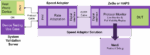
For protocols such as PCIe, relying on a standard host server as a test environment is not feasible. The limitation stems from the server’s BIOS, which enforces strict timeout settings. These timeouts are easily exceeded by the relatively long response times of an emulation system. Once triggered, the timeouts cause the validation process to stall or hang, preventing meaningful progress.
To achieve a complete ICE solution, this challenge must be addressed head-on. The answer lies in a purpose-built System Validation Server (see Fig. 2) equipped with a modified BIOS. By removing or adjusting the restrictive timeout parameters, the server can operate seamlessly with the slower responses of the emulated design.
Figure 2: System Validation Server for In-Circuit Emulation (Source: Synopsys)
This out-of-the-box solution offers immediate, practical benefits. Instead of spending months in back-and-forth iterations with an IT department to obtain and configure a host machine with a customized BIOS, validation teams can deploy a ready-made server that works from day one. The result is a dramatic reduction in setup overhead, faster time-to-validation, and a more reliable environment for exercising advanced protocols like PCIe under real-world conditions.
Ultra-High-Bandwidth Communication Channel
One of the most transformative advances in modern speed adapters is the introduction of ultra-high-bandwidth communication channels between the emulator and the adapter. Today’s leading-edge solutions can sustain throughput levels of up to 100 Gbps, enabling them to increase the overall validation throughput.
By approaching the communication rates of the real silicon, speed adapters allow engineers to stress-test SoCs under realistic workloads, validate protocol compliance at line rate, and observe system behavior under continuous, heavy traffic conditions.
Moreover, this capability ensures that networking-intensive applications, such as those found in data centers, 5G infrastructure, and high-performance computing systems, can be tested in environments that closely mimic deployment scenarios. The result is a dramatic increase in confidence that designs will not only function but also perform optimally once in the field.
Multi-user Deployment
A single speed adapter can be logically partitioned to support concurrent multi-user operation. The adapter’s port resources can be allocated in their entirety to a single user, or subdivided into up to three independent partitions, each assigned to a different user.
For instance, a 12-port Ethernet speed adapter may be configured as a monolithic resource (all 12 ports mapped to one user) or segmented into three logical groups of four ports each, enabling three users to access discrete subsets of the adapter in parallel.
The same partitioning capability applies to PCIe interfaces: the adapter can expose up to three independent PCIe links, each link operating in isolation and assigned to separate users. These features, resource partitioning, port multiplexing, and independent link allocation are natively supported in the architecture of the speed adapter.
Advanced buffering and flow-control techniques
The architectural refinements eliminated packet drops and ensured deterministic behavior across fast and slow clock domains. They also allowed speed adapters to scale with large verification workloads.
Conclusion
Today’s speed adapters combine flexible, multiuser deployment, stable and exceptionally fast high-speed links, deterministic flow control, improved DUT debuggability, proven resilience under continuous datacenter workloads. With these advances, third-generation speed adapters moved ICE from a niche verification mode into a mainstream, indispensable tool for system validation.
Today’s emulation platforms configured with this third generation of speed adapters finally bridge the gap between functional verification—which validates DUT functionality and I/O protocols—and system-level validation, which ensures that designs interact correctly with the physical world. This holistic approach closes a long-standing blind spot in hardware-assisted verification, enabling faster debug cycles, higher-quality silicon, and first-pass success in increasingly complex SoCs.
The concept of built-in self-test for electronics has been around for a while. An article in Electronic Design from 1996 declared that, “built-in self-test (BIST) is nothing new.” The memory subsystem is a particularly large and complex part of any semiconductor design, and it’s one that can be particularly vexing to test. Design teams have therefore applied the concepts of BIST to memories for quite a while as a result. Memory BIST has many advantages including better reliability, reduced manufacturing costs, and enhanced system performance. The complexity of implementing an effective memory BIST strategy has gotten quite challenging, however. The huge size and performance demands of memory systems contributes to this, as does the additional complexity of 3D IC design.
Siemens Digital Industries Software has been developing the Tessent™ MemoryBIST software and IP to deliver a complete solution for at-speed test, diagnosis, repair, debug and characterization of silicon memories of all types. The ability to address this broad class of problem with one comprehensive solution provides significant benefits. This platform has recently been extended to handle the unique requirements of embedded non-volatile RAM, or NVRAM. Since embedded NVRAM use is on the rise, this is a significant addition. Let’s examine the footprint of what Siemens delivers with a special focus on how Tessent MemoryBIST expands to include NVRAM.
Tessent MemoryBIST Overview
Some of the reasons that this platform is the Industry-leading solution for memory built-in self-test include its hierarchical architecture that enables the addition of built-in self-test and self-repair capabilities at both the individual core level and the top level. Both software and enabling IP are included.
The system delivers on-chip generated test vectors to memories at application clock frequencies. Tessent MemoryBIST controllers are configurable to support a variety of memory types, as well as a range of memory timing interfaces and port configurations. These are accessed and controlled through an IEEE 1687-2014 (IJTAG) network. This highly configurable network can access all Tessent IP and support any third-party IJTAG-compliant instruments. There is a lifecycle management aspect to this as well, since controllers can be accessed throughout the life of the device, including manufacturing test, silicon debug and in-system test. The figure below illustrates the hierarchical Tessent MemoryBIST infrastructure.
Hierarchical Tessent MemoryBIST infrastructure
There are many benefits provided by a system like this. Here are some:
Flexible and automated BIST IP integration, access network integration and pattern validation shorten time-to-market
Resource sharing and flow integration with Tessent LogicBIST and Tessent TestKompress reduce overall DFT cost and increase defect coverage
The option to use field programmable algorithm specifications allows complete control of test quality and test time trade-offs
User controllable area and test time trade-off options enable product-specific test cost optimization
On-chip global eFuse management and optional non-volatile memory test capability reduce overall manufacturing costs
Desktop-based test debug and characterization speed time-to-market
Customizable pass/fail criteria provided by the ECC option enhances yield and reliability
Works with ECC detection/correction capabilities to safeguard against aging defects
A Look at NVRAM Support
Thanks in part to the ubiquitous use of AI workloads in just about every design, the need for embedded NVRAM is growing significantly. While Flash has been the go-to approach for years, this technology doesn’t scale to advanced process nodes and so there are several new NVRAM technologies entering the market.
Etienne Racine
NVRAMs have very different test criteria and requirements, and so the need for BIST automation here is quite significant. That’s why the recent expansion of Tessent MemoryBIST to include NVRAM is so important. I had the opportunity to speak with Etienne Racine, the Product Manager for Tessent MemoryBIST at Siemens Digital Industries Software. Etienne has been working on silicon test solutions at Siemens and at Mentor before that for almost 18 years. Prior to Siemens and Mentor, he spent over a decade working on advanced test solutions, so Etienne brought a wealth of knowledge to the discussion.
Etienne explained that until recently there has been no well-developed BIST support for NVRAMs. This is why the additional capabilities of the Tessent suite are significant. We discussed access protocols and Etienne explained that the commands to operate embedded NVRAMs are quite different than those for embedded SRAMs. This means that the way BIST interfaces to the NVRAM must be changed. We also discussed the need to support trimming and trimming sequences. This process is similar to calibration.
He went on discuss the process of deployment of MRAMs, which is one of the newer embedded NVRAM technologies designed to replace Flash. For MRAMs, a trimming, or calibration step must be done before the device can be reliably used. The Tessent MemoryBIST NVM option provides these capabilities in an automated way. He also discussed the ability to define the required waveforms needed to test new NVRAM technologies. These waveforms can be described in the Tessent platform, paving the way for more efficient BIST strategies.
Looking ahead, Tessent MemoryBIST also provides support for testing memories that are external to the device containing the BIST IP. Support is provided for both stand-alone memory packages at the board level and 2.5/3D packages consisting of one or more memory dies stacked on top of a separate logic die. This strategy is summarized in the diagram below.
Testing 3D stacked memory die
To Learn More
My conversation with Etienne touched on many topics. There are a lot more capabilities delivered by the Tessent MemoryBIST software and IP. You can find many well packaged solutions to your MBIST requirements here. The good news is there is a comprehensive overview of the platform available. You can access your copy of Tessent MemoryBIST, memory self-test, repair and debug here. And that’s how Tessent MemoryBIST expands to include NVRAM.