webinar banner AI 2026 v2

CISCO ASIC Success with Synopsys SLM IPs

CISCO ASIC Success with Synopsys SLM IPs
by Daniel Nenni on 12-29-2025 at 10:00 am

cisco silicon one networking 839x473

Cisco’s relentless push toward higher-performance networking silicon has placed extraordinary demands on its ASIC design methodology. As transistor densities continue to rise across advanced SoCs, traditional design-time guardbands are no longer sufficient to ensure long-term reliability, consistent performance, and efficient power consumption. Instead, these chips require deep, real-time observability throughout the operational lifecycle. The challenge is addressed through Cisco’s adoption of Synopsys Silicon Lifecycle Management (SLM) IPs. The company’s latest Silicon One ASICs integrate a broad set of embedded monitors and analytics capabilities that collectively redefine what in-silicon visibility looks like.

Modern networking ASICs operate under highly dynamic conditions. Voltage and temperature fluctuate constantly inside dense logic blocks, and variations in process corners across a single die can influence timing behavior in subtle but meaningful ways. Cisco faces additional pressure because its chips target mission-critical infrastructure where uptime, predictability, and performance efficiency are paramount. According to the success story, transistor aging, exacerbated by thermal and voltage cycling, can reduce timing slack over time, making continuous monitoring essential to safeguard performance margins.

To address these challenges, Cisco deployed a comprehensive suite of Synopsys SLM IPs across its newest ASIC platforms. At the center of this strategy is the Process, Voltage, and Temperature Monitor (PVT) subsystem, orchestrated by the PVT Controller (PVTC). The PVTC aggregates data from multiple distributed sensors, enabling a unified view of environmental and process states across the chip. With this real-time data, the system can support dynamic voltage and frequency scaling, optimizing power and performance based on immediate conditions rather than worst-case assumptions.

Several sensor types feed into this controller. The Process Detector identifies variations across silicon regions, helping Cisco tune performance and understand die-to-die differences. Voltage Monitors track fluctuations in supply rails, ensuring critical blocks operate within safe thresholds. Distributed Temperature Sensors and thermal diodes provide granular thermal maps, improving both thermal management and temperature-dependent calibration. Collectively, these sensors give unprecedented visibility into what is happening inside every major functional quadrant of the ASIC.

Beyond PVT data, Cisco uses the Path Margin Monitor to watch critical timing paths in real time. Instead of relying solely on static timing analysis or margin-heavy design, PMM enables early detection of timing degradation due to aging or unexpected workload conditions. Meanwhile, the Clock Delay Monitor focuses on SRAM behavior, measuring access times and ensuring that memory blocks meet their intended timing specifications during actual operation.

The results are substantial. Cisco has achieved significantly enhanced real-time observability across its ASIC designs, enabling dynamic optimization of power and performance rather than fixed guard-banding. The continuous monitoring of path margins and aging allows proactive reliability management, helping extend the usable lifespan of the silicon. The insights generated not only improve today’s chips but also feed back into future design cycles, refining models and guiding architectural decisions. The modular nature of Synopsys SLM IPs also ensures Cisco can tailor sensor density and placement to each ASIC’s unique requirements, balancing efficiency with coverage.

Bottom line: Cisco plans to leverage Synopsys Silicon.da analytics to mine the vast data produced under diverse operating conditions. This data-driven feedback loop positions Cisco to continue advancing high-performance networking silicon while reducing risk and improving consistency across its product lines. Through its collaboration with Synopsys, Cisco has established a new benchmark for ASIC observability, reliability, and lifecycle optimization in the networking domain.

https://www.synopsys.com/success-stories/cisco-enhances-asic-slm.html
Also Read:

How PCIe Multistream Architecture Enables AI Connectivity at 64 GT/s and 128 GT/s

WEBINAR: How PCIe Multistream Architecture is Enabling AI Connectivity

Lessons from the DeepChip Wars: What a Decade-old Debate Teaches Us About Tech Evolution


RISC-V: Powering the Era of Intelligent General Computing

RISC-V: Powering the Era of Intelligent General Computing
by Daniel Nenni on 12-29-2025 at 8:00 am

Andes RISC V Summit 2025 Charlie Su

Charlie Su, President and CTO of Andes Technology, delivered a compelling keynote at the 2025 RISC-V Summit North America, asserting that RISC-V is primed to drive the burgeoning field of Intelligent General Computing. This emerging paradigm integrates AI and machine learning into everyday computing devices, from AI-enabled PCs and smartphones to edge servers, software-defined vehicles, and robotic platforms. Su emphasized that advancements in AI/ML are infusing intelligence into general-purpose computing, enabling applications in personal use, factory automation, surveillance, drones, and autonomous driving (ADAS Levels 0-4). He predicted that robots, as app-enabled platforms, could surpass the smartphone market in scale. To support this, Intelligent General Computing demands a robust ecosystem for both general-purpose tasks and large-scale AI/ML, encompassing software and hardware.

Charlie highlighted RISC-V‘s role in fostering innovations for large-scale AI/ML. A prime example is Meta’s Training and Inference Accelerator (MTIA), which leverages Andes’ vector and scalar cores alongside the Automated Custom Extension (ACE) framework, as detailed in ISCA 2023. Two generations of MTIA have been deployed in Meta’s data centers since 2023, based on RISC-V processors with automated extensions. Other accelerators using SRAM-based Compute-In-Memory include solutions for servers (e.g., RiVos AI SoC), cloud services (SAPEON), photonics-based AI, and ADAS systems. These are powered by Andes cores like AX46MPV, AX45MPV, NX27V, and AX65, demonstrating RISC-V’s versatility in high-performance AI.

The RISC-V software ecosystem is maturing rapidly, bolstered by initiatives like RISE (RISC-V Software Ecosystem), which accelerates open-source software development, improves quality, and aligns efforts for cloud and IoT devices. Java 22/21 support is already in place, with tools spanning compilers (LLVM, GCC, GLIBC), system libraries (FFmpeg, OpenBLAS), kernel/virtualization (Linux, Android, Performance Profiles), and more. Premier members include Andes, Google, Intel, NVIDIA, Qualcomm, and Samsung. Debian’s open-source support underscores this maturity, with RISC-V achieving a 98.4% successful build rate across over 64,000 packages—ranking third overall. Metanoia’s 5G O-RAN software architecture further exemplifies modular, full open-source releases for semi-turnkey solutions.

Andes’ processor lineup is tailored for this era. The AX46MPV offers powerful compute and efficient control, compliant with RVA22+ including AIA and SV38/48/57 virtualization. It features dual-issue for vector/scalar instructions, a Vector Processing Unit (VPU) with VLEN/DLEN from 128-1024 bits, supporting int4-int64 and bf16/fp16-64 formats, plus enhanced ReductionSum. Multicore support reaches 16 cores, with boosted memory via dual-issue load/store, strong outstanding capabilities, and a High-speed Vector Memory (HVM) interface handling multiple OOO requests. Performance gains over AX45MPV include ~18% in SpecInt2006 (5.65 score), over 2x in key vector libraries (libvec, libnn), and +40% bandwidth.

The AX66, a mid-range application processor, is RVA23 compliant with dual vector pipes (VLEN=128), 4-wide frontend decode, 128-entry ROB, 8 execution pipelines, and TAGE-L branch predictor. It supports up to 8 cores, 32MB shared L3 cache (mostly exclusive), and 128/256-bit AXI4 interfaces with IOMMU, APLIC, and CHI. Vector performance yields >10x in libnn key functions (9.6x average), >4x in libvec (3.55x average), and significant crypto boosts (4.7x SHA-256, 10.5x AES-128, 6.4x SM4). Bandwidth increases by 25%.

For high-end needs, the Cuzco series scales to 20 SpecInt2k6/GHz, with patented time-based scheduling via Time Resource Matrix for efficient instruction issuing and power reduction. RVA23 compliant, it features 8-wide decode, 256 ROB entries, 8 pipelines (2 per slice), advanced branch prediction, private L1/L2 caches, up to 256MB shared L3, multiprocessor up to 8 cores, and CHI/256-bit MMIO. Early 5nm implementation targets 2.5GHz, with current SpecInt2006 at ~18/GHz, using 7M gates for CPU and 4.5M for 2MB L2.

Andes enhances the ecosystem with AndesAIRE, an “AI Runs Everywhere” end-to-end solution, including IDEs, NN SDKs, compilers (MLIR, TVM), interpreters (ONNX Runtime, PyTorch), and accelerators like AndLA 1350. OS support is comprehensive: RISC-V specs (RVA22/23 profiles, SoC platforms), Linux distros (Debian, Fedora, Ubuntu, verified by Andes), upstream kernel features (strace/ftrace, Perf, HIGHMEM, CPU hotplug, ongoing Suspend-to-RAM and PowerBrake), bootloaders (U-Boot, OpenSBI), and RTOS (FreeRTOS, Zephyr, Thread-X).

Bottom line: Charlie noted Andes leads RISC-V IP shipments with rich portfolios. The latest processors—AX46MPV for compute/control, AX66 to Cuzco for performance—position Andes strongly. The RISC-V ecosystem is ready for Intelligent General Computing, promising transformative impacts across industries.

Contact Andes

Also Read:

Journey Back to 1981: David Patterson Recounts the Birth of RISC and Its Legacy in RISC-V

Google’s Road Trip to RISC-V at Warehouse Scale: Insights from Google’s Martin Dixon

Bridging Embedded and Cloud Worlds: AWS Solutions for RISC-V Development


Simulating Quantum Computers. Innovation in Verification

Simulating Quantum Computers. Innovation in Verification
by Bernard Murphy on 12-29-2025 at 6:00 am

Innovation New

Quantum algorithms must be simulated on classical computers to validate correct behavior, but this looks very different from classical logic simulation. Paul Cunningham (GM, Verification at Cadence), Raúl Camposano (Silicon Catalyst, entrepreneur, former Synopsys CTO and lecturer at Stanford, EE292A) and I continue our series on research ideas. As always, feedback welcome.

The Innovation

This month’s pick is How to Write a Simulator for Quantum Circuits from Scratch: A Tutorial. The authors are from École de Technologie Supérieure, Montreal and the University of Massachusetts. The paper was posted in June 2025 in arXiv.

Quantum simulators work on an abstraction – how qubits and “gates” are implemented is a fascinating topic but a distraction for this discussion. Our goal in this review is to introduce the topic of simulating quantum algorithms on a classical computer, because these methods are sufficiently disjoint from familiar classical computation to require an introduction before we move onto new research in this area.

This paper introduces a method to build a simulator for a small quantum computer (~20 qubits). It is supported by a web-based implementations and code walkthroughs to give a sense of how quantum simulation works. You should think of linear algebra methods to evaluate a circuit, multiplying an initial qubit vector by a series of tensors corresponding to gates in the circuit.

Paul’s view

Quantum venture funding is already well over $3B, rising fast and getting a lot of attention in the media. So what about verifying quantum circuits? First stop here is a quantum circuit simulator. Kudos to Bernard for finding a wonderfully written paper on this topic. It describes notations used for describing quantum circuits, both graphically and in equation form. It also works through the basic math needed to understand how a quantum simulator works. It’s an algorithmic level paper, not a paper on quantum physics.

In a digital circuit, each “bit” of state (a register or a wire) can be read and written independently. Logic simulators need to process transitions on registers and wires in time order, via an event queue, but this processing is local and need only consider the gates they are directly connected to.

In the quantum world “qu-bits” of state are “entangled” and need to be considered collectively as a single “state vector”. Simulating a quantum circuit proceeds like an analog circuit simulation where a vector of all the voltages or currents on each wire is formed, and simulation involves multiplying this vector with a matrix whose coefficients are determined by the circuit components and connectivity. For a circuit with n wires an analog simulator must multiply a 1 x n circuit state vector by an n x n simulation matrix derived from the circuit structure.

The cool thing about a quantum circuit is that a circuit with n qubits has a state vector with 2^n elements, one for each of the 2^n binary representations of n-bits. A quantum circuit performs operations simultaneously on all 2^n elements of this state vector, with means it conceptually operates in parallel on all 2^n possible values of the n qubits.

To simulate a quantum circuit with non-quantum digital hardware means multiplying a quantum state vector of size 2^n by a simulation matrix of size 2^n x 2^n, which is O(4^n) multiplications. The paper works through some neat algorithmic tricks based on some fundamental properties of quantum state vectors and simulation matrices that improves the runtime complexity to O(n.2^n). The elements of the state vector are floating point numbers, so the entire simulation maps very well to GPUs, e.g. this NVIDIA blog claims evaluating up to 36 qubits using eight A100s. Wow!

Each element in the state vector is a complex number, whose magnitude squared is the probability of the circuit being in that state. The sum of all the magnitude squared across the whole state vector is 1 and you can think of the state vector as representing a point on the surface of a 2^n dimensional hypersphere whose radius is 1. The goal of a typical quantum circuit algorithm is to use quantum gates to move the state vector around this hypersphere until it points almost perfectly along the axis of the dimension that is the desired result of the algorithm. Logic gates in digital circuits perform Boolean operations on state bits to calculate their result. Quantum gates rotate state vectors in various ways around their hypersphere. Developing a quantum algorithm requires figuring out a combination of rotational operations that move the state vector towards the desired result. Let’s see what Bernard can find published on what it means to verify these kinds of algorithm.

Raúl’s view

This month’s paper is a very nice, detailed tutorial on how to build a quantum circuit simulator using classical computing techniques, even with minimal prior knowledge of quantum mechanics. A simulator is verification 101; the purpose of creating a simulator from scratch is not as an alternative to existing open-source and commercial packages, but for a deeper understanding of quantum computing and the core algorithms necessary. It introduces essential quantum concepts and notations such as Dirac notation, state vectors, Hilbert space, tensor products, and the Bloch sphere, and quantum gates such as Hadamard, SWAP, Toffoli (CCNOT), Pauli X, Y and Z. Unlike physical quantum computers which collapse the state to 0 or 1 when measured, simulators can directly compute the complete state, including the probability of a 1 and the phase (Bloch sphere coordinates of each qubit). Measurement gates collapse the state and result in two new state vectors, corresponding to a measurement of 0 and 1.

The resulting simulator can handle up to ~20 qubits on a personal computer, utilizing roughly 1000–2000 lines of code in JavaScript (the largest quantum computer than can be simulated on a HPC is 50 qubits). An emphasis is placed on efficiency to handle the computational complexity associated with explicit matrix multiplication, in particular for Qubit-Wise Multiplication without explicitly forming the large layer matrices, but still O(2n nd) for d layers with n gates each; and SWAP, the exchange of the states of qubits simulated by directly manipulating the indices of the state vector’s amplitudes, also exponential in complexity. Further enhancements mentioned include adding robust error checking, implementing memory-saving in-place updates, and leveraging hardware acceleration via GPU programming.

I found the paper a great introduction to quantum computing. The online simulators help explain the basics, and the paper references commercial systems and more advanced research for readers interested in more detail.

Also Read:

Quantum Advantage is About the Algorithm, not the Computer

Quantum Computing Technologies and Challenges

Quantum Computing Algorithms and Applications


Kirin 9030 Hints at SMIC’s Possible Paths Toward >300 MTr/mm2 Without EUV

Kirin 9030 Hints at SMIC’s Possible Paths Toward >300 MTr/mm2 Without EUV
by Fred Chen on 12-28-2025 at 2:00 pm

Number of masks required for the M0 through M3 layers

Earlier this month, TechInsights did a teardown of the Kirin 9030 chip found in Huawei’s Mate 80 Pro Max [1]. Two clear statements were made on the findings: (1) the transistor density of SMIC’s “N+3” process was definitely below that of the earlier 5nm processes from Samsung and TSMC, and (2) metal pitch was aggressively scaled using DUV multi-patterning. Given that the density (formula defined in [2]) is less than 125 MTr/mm2 (Samsung 5LPE), corresponding to a track pitch of 36 nm and gate pitch of 54 nm [3], we can infer that it is the minimum metal pitch that was aggressively scaled, going beyond double patterning. In this article, we will go over the possible paths ahead for SMIC that could ultimately enable transistor densities >300 MTr/mm2, knowing that minimum metal pitch is now likely being patterned by some form of self-aligned quadruple patterning (SAQP).

Some Guiding Numbers for Pitch Scaling

The actual pitches for SMIC’s latest N+3 and previous N+2 processes were found by TechInsights but never revealed publicly. When those processes are discussed in this article, representative pitches will be used.

Thanks for reading Multiple Patterns! Subscribe for free to receive new posts and support my work.

It will be assumed that getting to >300 MTr/mm2 will follow the path shown in Table 1. At N+3, the M0 layer was shrunk aggressively; this will be repeated for M2 at N+4.

Table 1. Possible pitch shrink path from N+2 to >300 MTr/mm2. See text for explanations.

A number of clarifications are needed to explain the numbers used in Table 1.

The transistor density is calculated from the gate pitch and the track pitch, which is taken to be M2 here. We know that for N+3, the track metal is not the minimum pitch metal. The formula is the same as used in [2], with 60% weight on 4-transistor NAND cells covering 3 gate pitches, and 40% weight on a 32-transistor flip-flop covering 19 gate pitches. This gives [6*4/3+0.4*32/19]/(gate pitch*cell height)=1.474/(gate pitch*cell height) as the transistor density formula.

At the “2nm” node, the transition to buried power rail is expected, which enables the cell height to go from 6 tracks to 5 tracks.

For older nodes, M1 pitch can be less that gate pitch, e.g., 2/3 gate pitch, but 36 nm pitch with EUV has stochastic defect density concerns [4,5], so it has been expected that M1 pitch will be relaxed to the same as gate pitch.

A 44 nm gate pitch and 22 nm pitch with buried power rails allowing 5-track cells would be necessary to get over 300 MTr/mm2.

Different SAQP Approaches Proposed

Achieving a minimum metal pitch as small as 30 nm or smaller is no trivial feat. Two methods have been proposed by Huawei and SiCarrier.

Double SALELE

Huawei’s patent CN117751427 discloses what is essentially the SALELE [6] approach applied twice. “SALELE” stands for “self-aligned litho-etch-litho-etch;” it is a more sophisticated version of the traditional litho-etch-litho-etch double patterning approach. Double SALELE means doing SALELE twice to get the quadruple patterning effect (Figure 1).

Figure 1. Double SALELE approach. Left: First litho-etch (blue), followed by spacer (gray), then etch block/cut (yellow). Center: Second litho-etch (green), followed by etch block/cut (purple). This completes the first SALELE. Right: Second SALELE completed.

In the SALELE approach, sidewall spacers are applied to a first set of lines, formed conventionally, by “litho-etch.” Then these lines may be cut using etch blocks patterned by a second mask. A third mask is used to pattern the second set of lines, with alignment assisted by the sidewall spacers. Then, this second let of lines is cut, using a fourth mask.

This approach consumes an excessive number of masks. Four masks are needed for four sets of lines, so that each line printed by a given mask is separated by sufficient distance (≥ minimum allowed pitch). Four additional masks are needed for the etch block/cut locations, corresponding to each of the four sets of lines. This gives a total of eight masks! Fortunately, this is not the only approach.

Double SADP

SiCarrier’s patent CN117080054 [7] discloses an SAQP-class approach that uses half the number of masks used for double SALELE. In a way, it is a kind of cascaded, double self-aligned double patterning (SADP) (Figure 2).

Figure 2. Double SADP approach. Left: First spacers (gray) are formed on sidewall of mandrel pattern (blue). Center left: Etch block/cut (black) is applied to the spacer pattern. This completes the first SADP. Center right: Second spacers (yellow) are formed on the sidewalls of the first spacer pattern, followed by a gap fill (green). Etch block/cut (red) is applied to the gap fill pattern. This completes the second SADP. Right: Wide features are formed with a separate (fourth) mask.

The first SADP leaves a set of first spacers which correspond to the first set of metal lines. The gaps left after the second follow-on SADP correspond to the second set of metal lines. Wide metal lines are completed at the end. Like in SALELE, the two sets of lines are cut separately. However, SADP enables twice the line density compared to a single litho-etch, and the cuts can also be made two lines at a time. Thus, the number of masks is halved from 8 to 4.

Diagonal FSAV Grid Becomes a Must

With metal pitches of 30 nm or less, metal linewidths become 15 nm or less. It is actually difficult to focus, even with High-NA EUV, down to a spot as small as this; the Rayleigh resolution limit would be 0.61 wavelength/NA = 0.61*13.5/0.55 = 15 nm. But looking ahead to the sub-2nm node, stochastics will become the overwhelming reason why even with High-NA EUV, directly printing a via is not feasible (Figure 3).

Figure 3. Absorbed photon density (1 nm pixel) for a 22 nm x 11 nm via on 44 nm x 22 nm pitch, with 6 mJ/cm2 absorbed EUV dose.

Lithographic difficulty has been a key driving reason for using diagonal via grids [8]. The minimum via pitch at advanced nodes cannot be as small as the minimum metal line pitch (Figure 4). Routing doesn’t require it anyway [8,9].

Figure 4. Left: The minimum via pitch cannot be as small as the minimum metal line pitch. Right: Diagonal via locations could be allowed.

It will become necessary to fill the intersection area between vertically adjacent metal layers, using the fully self-aligned via process [10]. A focused EUV spot will be wider than the metal linewidth at 3nm and below.

Based on the pitches in Table 1, we can predict the maximum number of masks used for patterning the V0, V1, and V2 layers. With ArF immersion, we allow 80 nm distance between vias [11]. Brute force via multipatterning will result in up to four masks used (Figure 5). A more efficient approach that fits the diagonal via grid is to use LELE double patterning to print portions of diagonal lines that cover the targeted via locations; a third mask would be used if needed to trim the portions if necessary.

Figure 5. Via multipatterning options. Each color represents a different mask. Top left: double patterning is sufficient for N+2, and some via layers of N+3. Top right: triple patterning would become necessary for N+4 and N+5. Bottom left: for N+6, quadruple patterning would become a necessary allowance if still using brute force multipatterning. Bottom right: Diagonal LELE (plus trim mask if necessary) is most efficient for accommodating the diagonal via grid.

Counting Cuts

Besides vias, metal line cuts add significantly to the mask count. For the M0 and M2 layers, the double SADP approach only requires two cut masks, while the double SALELE approach depends on the node pitches. The distances between cuts follow the same rules as for the vias. It could go up to four masks for the 1.x nm node (Figure 6).

Figure 6. Cut mask count for double SALELE metal layers. Each color represents a different mask.

The M1 and M3 layers are likely patterned by SALELE, so that narrow straight line cuts may be used to cut alternate lines, skipping lines in between. This would mean up to four masks (Figure 7).

Figure 7. Cut mask count for the SALELE metal layers (M1 and M3). Each color represents a different mask.

For EUV, SALELE cuts would still require two masks. Thus, DUV quadruple patterning for this purpose is still cheaper than EUV double patterning [12].

Smooth Ride Forward?

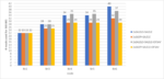
When the mask count increases for the M0 through M3 layers are tallied up for the different possible approaches, we get the overall result in Figure 8.

Figure 8. Number of masks required for the M0 through M3 layers for the representative nodes N+2 through N+6, for the different possible multipatterning combinations. “2xSALELE” = double SALELE, “2xSADP” = double SADP, “DFSAV” = diagonal line LELE on FSAV, with trim mask. SALELE is assumed applied to the M1 and M3 layers.

The double SALELE approaches will consistently require more masks than the double SADP approaches. The use of diagonal line double patterning with trim mask on FSAV saves three masks for N+6 (44 nm pitch M1, 22 nm pitch M0 and M2). In the best case, only 7 masks have been incrementally added from N+2 to N+4, and the total remained unchanged until N+6. This is to be compared with the worst case, where the mask count increase from N+2 continued after N+5, leading up to 18 masks for N+6.

N+5 is seen to be a convenient shrink of N+4, with no added masks.

Thus, the multipatterning path must be carefully planned several nodes ahead in advance in order to ensure that mask count increase can be manageable.

References

[1] R. Krishnamurthy, “SMIC Steps Toward 5nm: Kirin 9030 Analysis Shows the Foundry’s N+3 Progress,” TechInsights.

[2] Skyjuice, “The Truth of TSMC 5nm,” Angstronomics.

[3] D. Schor, “Samsung 5 nm and 4 nm Update,” Wikichip Fuse.

[4] Y. Li, Q. Wu, Y. Zhao, “A Simulation Study for Typical Design Rule Patterns and Stochastic Printing Failures in a 5 nm Logic Process with EUV Lithography,” CSTIC 2020.

[5] Y-P. Tsai, C-M. Chang, Y-H. Chang, A. Oak, D. Trivkovic, R-H. Kim, “Study of EUV stochastic defect on wafer yield,” Proc. SPIE 12954, 1295404 (2024).

[6] Y. Drissi, W. Gillijns, J. U. Lee, R. R-H. Kim, A. Hamed-Fatehy, R. Kotb, R. N. Sejpal, F. Germain, J. Word, “SALELE Process from Theory to Fabrication,” Proc. SPIE 10962, 109620V (2019).

[7] F. Chen, “SiCarrier’s SAQP-Class Patterning Technique: a Potential Domestic Solution for China’s 5nm and Beyond,” Multiple Patterns.

[8] S-W. Peng, C-M. Hsiao, C-H. Chang, J-T. Tzeng, US Patent Application 20230387002; Y-C. Xiao, W. M. Chan, K-H. Hsieh, US Patent 9530727.

[9] F. Chen, “Exploring Grid-Assisted Multipatterning Scenarios for 10A-14A Nodes,” Multiple Patterns.

[10] J-H. Franke, M. Gallagher, G. Murdoch, S. Halder, A. Juncker, W. Clark, “EPE analysis of sub-N10 BEoL flow with and without fully self-aligned via using Coventor SEMulator3D,” Proc. SPIE 10145, 1014529 (2017).

[11] M. Burkhardt, Y. Xu, H. Tsai, A. Tritchkov, J. Mellmann, “Ultimate 2D Resolution Printing with Negative Tone Development,” Proc. SPIE 9780. 97800E (2016).


Podcast EP324: How Dassault Systèmes is Creating the Next Generation of Semiconductor Design and Manufacturing with John Maculley

Podcast EP324: How Dassault Systèmes is Creating the Next Generation of Semiconductor Design and Manufacturing with John Maculley
by Daniel Nenni on 12-26-2025 at 10:00 am

Daniel is joined by John Maculley, Global High-Tech Industry Strategy Consultant at Dassault Systèmes. John has over 20 years of experience advancing innovation across the semiconductor and electronics sectors. Based in Silicon Valley, he works with leading foundries, OSATs, design houses, and research institutes worldwide to accelerate technology co-optimization and strengthen ecosystem resilience.

In this informative and forward-looking discussion, Dan explores the evolving focus on what kind of IP is curated and leveraged in the semiconductor industry with John, who describes knowledge and know-how as the new strategic differentiating IP for many companies. He explains why the ability to codify and curate this information across the enterprise is becoming quite valuable. John describes how IP management is now shifting to governance and intelligence, and with AI-augmented IP engineers can now design with a focus on manufacturability.

John discusses many other benefits of the work Dassault Systèmes is doing to facilitate an AI-augmented future for the semiconductor industry. Methods to capture institutional knowledge and make it available to all members of the team are discussed. The impact to design productivity for advanced 3DIC systems is significant.

The views, thoughts, and opinions expressed in these podcasts belong solely to the speaker, and not to the speaker’s employer, organization, committee or any other group or individual.


Why TSMC is Known as the Trusted Foundry

Why TSMC is Known as the Trusted Foundry
by Daniel Nenni on 12-26-2025 at 6:00 am

TSMC Ivey Fab

Taiwan Semiconductor Manufacturing Company (TSMC) is widely regarded as the world’s most trusted semiconductor foundry, a reputation built over decades through technological leadership, business model discipline, operational excellence, and reliability. In an industry where trust is as critical as transistor density, TSMC has become the backbone of the global digital economy.

First and foremost, TSMC’s pure-play foundry model is the foundation of its trustworthiness. Unlike integrated device manufacturers (IDMs) such as Intel and Samsung, which design and manufacture their own chips, TSMC does not compete with its customers. It manufactures chips exclusively for third parties and has maintained a strict firewall between customer designs. This neutrality reassures customers, from Apple and NVIDIA to AMD, Qualcomm, and countless startups, that their intellectual property will not be used against them. Over time, this consistency has created deep confidence across a vast ecosystem, making TSMC the default manufacturing partner for the world’s most valuable chip designers.

Second, TSMC’s technological leadership reinforces that trust. The company has consistently been first, or decisively best, to mass-produce advanced process nodes such as 7nm, 5nm, and 3nm at high yields. In semiconductor manufacturing, reliability is not just about innovation, but about delivering that innovation at scale, on schedule, and with predictable silicon. TSMC’s ability to translate cutting-edge research into stable, high-volume production has made it indispensable for customers whose product cycles depend on certainty. When companies commit billions of dollars to a chip design, they need confidence that the foundry can deliver exactly as promised and TSMC has repeatedly proven it can.

Third, manufacturing excellence and yield consistency distinguish TSMC from competitors. Advanced chips are extraordinarily complex, and small variations can destroy profitability or product viability. TSMC’s laser focus on process control, defect reduction, and continuous improvement results in industry-leading yields. High yields mean lower costs for customers, faster ramp-ups, and fewer surprises after tape-out. This operational discipline is a major reason customers trust TSMC with their most advanced and sensitive designs.

Fourth, TSMC has built a reputation for strong intellectual property protection and confidentiality. Semiconductor designs represent years of research and billions in investment. TSMC has demonstrated, across thousands of customers, that it can securely handle highly confidential data without leaks or misuse. This trust is reinforced by TSMC’s internal culture, strict access controls, and long-standing customer relationships. In an era of increasing cyber and industrial espionage, this reliability is invaluable.

Fifth, TSMC’s scale and ecosystem integration create trust through inevitability. The company has invested hundreds of billions of dollars in fabrication plants, equipment, and talent, creating manufacturing capabilities that few others can match. Its close collaboration with equipment suppliers (such as ASML and Applied Materials), EDA vendors (Synopsys, Cadence, Siemens EDA), and IP companies (Synopsys, Arm, Analog Bits) also known as the Grand Alliance allows customers to design within a mature, silicon-proven and well-supported ecosystem. This reduces risk and shortens time-to-market, further cementing TSMC as the safest choice.

Sixth, TSMC’s long-term strategic thinking strengthens customer confidence. The company invests aggressively ahead of demand, often years before returns are guaranteed. This willingness to absorb risk ensures that capacity is available when customers need it, even during industry upcycles or shortages. During recent global chip shortages, TSMC’s capacity planning and prioritization reinforced its image as a stable, responsible industry steward.

Finally, TSMC’s global credibility and governance matter. While geopolitical risks exist, TSMC has demonstrated transparency, regulatory compliance, and cooperation with governments and customers worldwide. Its expansion into the United States, Japan, and Europe reflects a commitment to supply chain resilience and global trust.

Bottom line: TSMC is the trusted foundry not because of a single advantage, but because of a rare combination: neutrality, technological supremacy, manufacturing reliability, IP protection, scale, and long-term vision. In an industry where failure is catastrophic and trust is earned slowly, TSMC has become the gold standard and the cornerstone of modern semiconductor manufacturing.

Also Read:

TSMC’s Customized Technical Documentation Platform Enhances Customer Experience

A Brief History of TSMC Through 2025

Cerebras AI Inference Wins Demo of the Year Award at TSMC North America Technology Symposium


Journey Back to 1981: David Patterson Recounts the Birth of RISC and Its Legacy in RISC-V

Journey Back to 1981: David Patterson Recounts the Birth of RISC and Its Legacy in RISC-V
by Daniel Nenni on 12-25-2025 at 10:00 am

RISC V Summit 2025 David Patterson

In a warmly received keynote at the RISC-V Summit, computer architecture legend David Patterson took the audience on a captivating trip back to 1981, using scanned versions of his original overhead transparencies to recount the birth of Reduced Instruction Set Computing (RISC) at UC Berkeley.

Patterson began with humor, noting his wife’s love for time-travel movies and explaining how age allows easy travel backward. Digging through old files, he rediscovered those classic plastic slides, artifacts unfamiliar to much of the younger audience, and used them to recreate the talk he gave across campuses over four decades ago.

The computing landscape of February 1981 was starkly different: mainframes and minicomputers dominated serious work, with IBM as the undisputed leader. DEC’s VAX, a refrigerator-sized 32-bit minicomputer running at 5 MHz with a 2 KB cache, represented the pinnacle. The IBM PC had not yet launched, and Intel’s 8086 was the cutting-edge 16-bit microprocessor. Cultural markers included Ronald Reagan’s presidency, disco music, and the release of Raiders of the Lost Ark.

Against this backdrop, Complex Instruction Set Computers (CISC) reigned supreme. The prevailing philosophy held that richer, more varied instructions would close the “semantic gap” between high-level languages and hardware. Microprogramming, enabled by growing memory densities under Moore’s Law, made complex instructions seemingly inexpensive. Marketing reinforced the idea that sophistication meant smaller programs and greater reliability, while registers were dismissed as old-fashioned.

Reality proved otherwise. High-level language programming used only a small subset of instructions. Complex operations, such as the VAX’s array-indexing instruction or IBM 370’s multi-register moves, were often slower than sequences of simpler ones. Design cycles lengthened dramatically, and microcode bugs were rampant; Patterson’s 1979–1980 sabbatical at DEC exposed constant patching of VAX microcode.

These observations crystallized into RISC principles: favor simplicity unless a compelling reason exists; prioritize fast clock cycles, easy decoding, and pipelining over instruction count or program size; recognize that microcode offers no magic; and rely on advancing compiler technology.

To illustrate, Patterson, a car enthusiast, likened CISC to an over-ornamented 1950s Cadillac and RISC to a sleek, agile sports car.

The ideas gained traction with Patterson and student David Ditzel’s 1980 paper, “The Case for the Reduced Instruction Set Computer,” published alongside a rebuttal from VAX architects—sparking immediate controversy and lively RISC vs. CISC debates at conferences.

Berkeley proved the concept through graduate courses. Leveraging DARPA-funded CAD tools, a simplified instruction set, and sheer beginner’s luck, roughly a dozen students designed, laid out, fabricated, and tested RISC-I in under two years. Remarkably, the RISC-I instruction set closely resembles today’s RISC-V core—Patterson called RISC-V’s version slightly more elegant.

Porting Berkeley UNIX was straightforward, and early benchmarks showed the student-built RISC-I roughly twice as fast as the professional, multi-year VAX effort—a stunning validation.

Patterson closed by honoring the original team, including faculty Carlo Séquin and John Ousterhout, and graduate students. He shared photos from a 2015 ceremony installing a plaque for the first RISC microprocessor, where RISC-I pioneers met RISC-V leaders, creating a touching cross-generational moment.

Bottom line: Forty-five years later, the simplicity and elegance born in those Berkeley classrooms power billions of devices worldwide and live on vibrantly in the open RISC-V ecosystem.

Also Read:

Google’s Road Trip to RISC-V at Warehouse Scale: Insights from Google’s Martin Dixon

Bridging Embedded and Cloud Worlds: AWS Solutions for RISC-V Development

The RISC-V Revolution: Insights from the 2025 Summits and Andes Technology’s Pivotal Role


Assertion-First Hardware Design and Formal Verification Services

Assertion-First Hardware Design and Formal Verification Services
by Kalar Rajendiran on 12-25-2025 at 6:00 am

LUBIS EDA Modelling

Generative AI has transformed software development, enabling entire applications to be built in minutes. But despite similar progress in AI-generated RTL, hardware verification remains a major bottleneck. RTL can be produced quickly, yet proving its correctness is extraordinarily difficult. This has revived a long-standing but historically unattainable idea, namely, a complete set of formal properties. Hardware design in RTL should begin with Assertion IP that precisely define the intended behavior of the design, rather than generated after the fact. For decades, this approach was out of reach. Today, the landscape has shifted, making assertion-first hardware design increasingly viable.

Tobias Ludwig, CEO of LUBIS EDA addressed this very topic at the Verification Futures Conference recently held in Austin, Texas. His talk covered how the company is moving the industry toward this long-awaited direction.

AI Can Generate RTL But Verification Is Still the Bottleneck

AI-generated RTL may look plausible, but correctness in hardware is a hard requirement. Chips must work under every possible condition, and AI systems trained on similar datasets often share similar failure patterns. Using AI to verify AI does not eliminate risk but rather compounds it. Verification continues to dominate engineering cost and schedule because ensuring correctness requires precise, formalized intent. Assertion IP provides that precision, but historically it has been too difficult to produce at scale.

Assertion IP: What Hardware Design Should Have Started With

Assertion IP captures design intent in its most accurate form. It describes how the design must behave across states, cycles, inputs, and transitions. In an ideal process, assertions would come first, serving as the specification against which RTL is implemented and proven. This would eliminate ambiguity and allow mathematical verification throughout development.

Why Hardware Has Not Started From Assertions

Creating a complete assertion set manually was impractical. Writing hundreds or thousands of assertions by hand was slow and error-prone. High-level modeling languages were inconsistent, lacked structure and were difficult to analyze. Property generation tools did not exist. And Formal Verification engines lacked the computational strength to handle the depth and complexity of real IP blocks.

While waiting for tools capable of generating Assertion IP automatically, the industry’s culture centered on “RTL-first,” with assertions treated as an afterthought rather than the foundation.

What Has Changed Now

The situation has changed dramatically. High-level model analysis engines can now extract states, transitions, invariants, and dataflow from C++/SystemC models. Automated property generation tools can transform these models into complete assertion suites that capture timing behavior, and correctness requirements. Formal verification engines have grown powerful enough to handle deep pipelines, cryptographic algorithms, and large state spaces. AI assistance now makes creating structured models easier, allowing engineers to translate natural-language intent into analyzable code. Together, these breakthroughs make assertion-first design far more practical than ever before.

Where LUBIS EDA Fits In: Opening the Window to Assertion-First Design

LUBIS EDA is turning this renewed possibility into a practical methodology. Its technology automatically generates comprehensive Assertion IP from high-level executable models, bridging the gap between abstract model and RTL implementation. Through refinement techniques that align abstract models with cycle-accurate RTL, LUBIS ensures that properties reflect bit-level reality.

Alongside the company’s formal verification services, LUBIS EDA provides training that help teams adopt assertion-driven workflows and achieve formal sign-off on complex blocks. As AI accelerates RTL generation, LUBIS EDA’s model-first, property-driven approach becomes essential for ensuring correctness and preventing hidden bugs.

Summary

For the first time, hardware teams can move toward a design process where intent is explicit, properties are complete and RTL correctness is provable from the start. This paradigm is now within reach thanks to advances in modeling, property generation, formal tools, and AI support. LUBIS EDA is helping the industry make this transition, prying open the door to a future where hardware design can begin with formal assertion IP.

To learn more, visit www.lubis-eda.com

Also Read:

Assertion IP (AIP) for Improved Design Verification

LUBIS EDA at the 2025 Design Automation Conference #62DAC

Automating Formal Verification


TSMC’s Customized Technical Documentation Platform Enhances Customer Experience

TSMC’s Customized Technical Documentation Platform Enhances Customer Experience
by Daniel Nenni on 12-24-2025 at 10:00 am

TSMC Online 2025

Taiwan Semiconductor Manufacturing Company, the world’s leading dedicated semiconductor foundry, has long prioritized customer-centric innovation to maintain its competitive edge in a rapidly evolving industry. TSMC is known as “The Trusted Foundry” for this reason.

Amid increasing complexity in chip design and manufacturing, driven by advanced nodes like 3nm and beyond, TSMC recognized the need for more efficient digital tools to support its global clientele. In response, the company upgraded its flagship customer self-service portal, TSMC-Online™, transforming it into a sophisticated Customized Technical Documentation Platform that significantly enhances user experience and operational efficiency.

Launched with upgrades beginning in April 2021, this platform embodies TSMC’s philosophy of being “Everyone’s Foundry.” The core objective was to address challenges posed by escalating technology and design intricacies, where customers from fabless designers to major tech giants require seamless access to vast amounts of technical data. Previously, navigating extensive documentation and production updates often demanded significant time and occasional support from TSMC’s customer service teams. The revamped TSMC-Online™ introduces a customer-oriented architecture, creating a truly customized service environment that empowers users to manage information as if operating their own fabrication facility.

Key enhancements revolve around three innovative methods:

A standard operation interface, personalized workspace, and intelligent guidance service. The standard operation interface provides a unified, intuitive layout that simplifies navigation across diverse functions, reducing learning curves and minimizing errors. Users benefit from consistent workflows, whether querying process design kits (PDKs), foundation IPs, or real-time wafer status updates.

The personalized workspace stands out as a hallmark of customization. Customers can tailor their dashboards with widgets aligned to specific roles and project stages—such as design verification, tape-out preparation, or manufacturing monitoring. For instance, engineers focused on advanced packaging like 3DFabric™ can prioritize relevant tools, while those in automotive applications highlight AEC-Q100 qualified resources. This flexibility accommodates varied stakeholder needs within a single organization, streamlining collaboration and boosting productivity.

Complementing these is the intelligent guidance service, which leverages smart features like contextual tutorials, animated walkthroughs, and real-time assistance modules. Previously, over half of users reportedly sought external help for document-related tasks due to platform complexity. Now, embedded animations and AI-driven prompts enable self-guided exploration, allowing instant access to tutorials without waiting for support, crucial across time zones.

Security remains paramount, with robust confidential information protection mechanisms ensuring sensitive data, including proprietary designs and production metrics, stays secure. Customers gain comprehensive visibility into the entire lifecycle, from design enablement through wafer manufacturing to shipment, fostering trust and operational transparency.

The impact has been profound. By January 2023, TSMC-Online™ averaged over 3,000 daily logins, reflecting high adoption and reliance. This digital collaboration tool accelerates product success by shortening time-to-market, reducing dependency on manual interventions, and enabling innovative outcomes in high-growth sectors like mobile, high-performance computing, AI, automotive electronics, and IoT.

TSMC’s commitment extends beyond this platform; it integrates with broader initiatives like the Open Innovation Platform® (OIP), which includes ecosystems for EDA tools, IPs, and cloud-based design environments. However, the Customized Technical Documentation Platform within TSMC-Online™ directly tackles day-to-day pain points, exemplifying how digital transformation can elevate service quality in semiconductor manufacturing.

Bottom Line: In an era where speed and precision define success, TSMC’s platform not only optimizes customer experience but also strengthens partnerships. By continuing to refine these tools, TSMC reinforces its role as a trusted enabler of global technological advancement, ensuring customers can focus on innovation while the foundry handles the complexities.

Also Read:

Cerebras AI Inference Wins Demo of the Year Award at TSMC North America Technology Symposium

TSMC Formally Sues Ex-SVP Over Alleged Transfer of Trade Secrets to Intel

TSMC Kumamoto: Pioneering Japan’s Semiconductor Revival


The 10 Practical Steps to Model and Design a Complex SoC: Insights from Aion Silicon

The 10 Practical Steps to Model and Design a Complex SoC: Insights from Aion Silicon
by Daniel Nenni on 12-24-2025 at 6:00 am

10 Practical SoC Steps AION Silicon

In the fast-evolving world of semiconductor design, creating a complex System-on-Chip (SoC) requires meticulous planning to ensure performance, power efficiency, and cost-effectiveness. Aion Silicon’s white paper, authored by Piyush Singh, outlines a streamlined methodology that leverages advanced modeling to bridge the gap from abstract concepts to silicon-ready specifications. Drawing on proprietary tools built atop EDA solutions from Arm and Synopsys, the paper emphasizes early architectural validation to mitigate risks and accelerate time-to-market. This approach is particularly vital for domains like AI, automotive, and high-performance computing, where SoCs integrate diverse components such as CPUs, GPUs, DSPs, and custom IP.

The white paper begins with an overview of SoC modeling’s role in preempting design flaws. Before placing any transistors, accurate models assess key metrics like bandwidth, latency, and Network-on-Chip (NoC) configuration. Aion Silicon’s custom modeling flow enhances vendor tools with extensive tweakable settings, enabling rapid iterations. Unlike traditional spreadsheet-based methods that take months, this flow delivers insights in days, allowing quick evaluation of variants to match customer use cases.

A core section explains how an ASIC evolves from an abstract view, depicted as application tasks on initiators (hardware blocks generating traffic) and targets (memory receivers), to a detailed specification. Central to this is the interconnect fabric, which connects compute and memory elements. Its design remains fluid until floor planning, influenced by timing constraints and die layout. Modeling provides a starting point, refining the NoC iteratively.

The paper highlights modeling’s advantages: estimating architecture, playing “what-if” scenarios, and enabling early software development. It categorizes modeling types, from dataflow (MATLAB / Python / C++ algorithms without timing) to loosely timed (for software prototyping) and approximately timed/fast timed models (ideal for exploration with transaction-level tracing). Cycle-accurate RTL simulations, while precise, are too slow for initial analysis.

Performance exploration is deemed essential because IP blocks, validated in isolation, face real-world constraints when integrated. Other blocks’ traffic patterns impact interconnect and memory, necessitating simulations to size subsystems appropriately.

The heart of the white paper is the “10 Steps to Architecture Success,” a phased approach breaking down complexity. The first four steps are analytical, often spreadsheet-based:

  1. System OI Analysis: Examine input/output dataflows, including burstiness, latency, timing, and formatting to determine buffer needs.
  2. Processing Analysis: Decompose algorithms into sub-tasks, grouping functionalities (e.g., MPEG decode and image analysis).
  3. IP Analysis: Identify third-party IP blocks, incorporating datasheet details on memory and compute requirements for accurate modeling.
  4. Data Interchange Analysis: Decide data exchange methods—on-chip SRAM/FIFO for small data or external DDR for large—based on size and access frequency.
The remaining steps shift to simulation:
  1. Workflow Model (Transactional): Create software representations of algorithm stages as simulation objects (e.g., green boxes in diagrams) with latency/processing settings, connected by channels for sequencing.
  2. Simulate to Verify Processing: Run simulations to visually confirm algorithm sequencing using modeling tools’ visualization features.
  3. Quantify Data Interchange: Model hardware with Virtual Processor Units (VPUs) and local memory, defining communication domains and verifying configurations.
  4. Data Physical Exchange: Remodel memory as external via a common controller, enhancing connectivity accuracy.
  5. Implement Interconnect: Add NoC fabric, replacing direct connections, and evaluate timing/performance impacts, iterating as needed.
  6. Optimize Performance: Adjust settings to identify bottlenecks, reduce latency, and improve throughput through quick simulations (minutes to hours).

These steps progressively refine models, eliminating dead ends and focusing resources logically. The paper concludes with Aion Silicon’s profile: founded in 2002, it offers end-to-end ASIC/SoC services across global centers, emphasizing first-time-right silicon.

Bottom line: This methodology underscores modeling’s transformative power in SoC design, reducing project risks and fostering innovation. By integrating custom flows with established EDA tools, Aion Silicon empowers designers to deliver optimized chips efficiently, proving that a structured path from abstraction to reality is key to semiconductor success.

See more AION Silicon Whitepapers here.

Also Read:

Live Webinar: Considerations When Architecting Your Next SoC: NoC with Arteris and Aion Silicon

Architecting Your Next SoC: Join the Live Discussion on Tradeoffs, IP, and Ecosystem Realities

The Sondrel transformation to Aion SIlicon!