The Doctrine of Eternal Recurrence- (Nietzsche..) Deja’ Vu all over again…
The semiconductor industry has seen this movie before, several times….new entrant into the memory chip industry, disrupts the status quo and goes on to dominate the industry (until the next new entrant…)
The Japanese did it to the American chip industry; The Koreans did it to the Japanese; And now China will do it to the Korean chip industry…. And don’t forget about Taiwan in here as well….
Back in ancient chip industry history there used to be more than seven US manufacturers of DRAM (Intel, IBM, Motorola, Micron, Mostek National & TI) now there is only one left as Japan pushed the US out of the DRAM business….
Japan lost out to Korea as Japanese chip engineers spent their time off on weekends in Korea, making a few extra Yen by transferring know how and secrets to brand new , start up, Korean DRAM manufacturers.
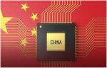
We are likely at the beginning of China entering the memory market to eventually displace the existing Korean dominance. China has bought, begged, borrowed or stolen memory technology to get there
Many currently say it will never happen, or it will take too long or China will never get the technology or the manufacturing right but those statements have been heard before in the US and Japan (just before they lost their chip dominance at the time…) and we know how the movie ended…
China memory makers are share driven , not profit driven…
One key factor that must be understood is that a new entrant to a market (in not just the chip market..) is not driven by profitability but by market share and total revenue even at the expense of profits…..
Existing players want to maintain profitability and will cede market share to try to maintain profitability.
We have seen this before and see it every day in other “commodity like” markets that memory emulates.
China’s initial production of memory chips has nothing to do with profitability and everything to do with self-reliance in chips and the long game of market share and eventual market dominance.
China certainly has the resources and deep pockets to sell at a loss for a very long time in order to gain more than a foothold in the memory chip market.
In other words it really doesn’t matter if China can make memory chips on a cost competitive basis, it only matters that it can make them (which it seems to be doing)
Manufacturing at a profit can come later…much later
It doesn’t take a lot to upset the delicate supply/demand balance in the memory chip market
Much like the other giant, global, “commodity like” market , oil, the balance between supply and demand is a both very crucial and delicate balancing act that the industry maintains by ongoing , daily tweaking of supply to match the ever changing demand appetite of the global market.
Think of two heavy, giant elephants, one supply and one demand, in perfect balance on a seesaw….it doesn’t take a lot of weight, on either side, to throw the system out of balance and quickly impact stability (pricing and profitability).
Perfect equilibrium of supply and demand in the memory chip market is tough, if not impossible to achieve (much like the oil market) especially when you consider that the oil market has OPEC to regulate supply and the memory market seems to do it on an Ad Hoc basis (except for when the memory chip makers were caught conspiring…)
Memory makers have been pruning supply for over a year to try to get back in balance which it seems we are finally close to achieving.
With China entering the memory market, it would not take a lot of supply to destabilize the existing balance that the industry has worked so hard to achieve. Existing memory makers would have to cut production even further (and idle more semiconductor equipment tools…) to accommodate a new supplier to the market.
There have been some good past studies and analysis of the financial and competitive dynamics of the memory market
MIT study of the DRAM Market
China is further along in memory chips than expected
When theres a will theres a way……
I have heard a lot of people say that China will never catch up with Korean or other memory makers…we think that is a very short sighted statement that has been proven wrong in similar previous instances.
For those who doubted where China would be or where they would get memory technology we would point to Innotron (Now ChangXin Memory) which claims to be producing 20,000 19NM wafers of DRAM a month with capacity slated to double to 40,000 wafers per month by Q2 2020.
While 20,000 wafers per month is not a lot, getting to 40,000 a month starts to feel like enough to impact the current delicate, almost equilibrium in DRAM.
We think the impact of China on the DRAM market is not as far away as people think . How long will it take for ChangXin to get to 100,000 DRAM wafers a month?
Article on ChangXin memory
Even if this is an exaggeration that we commonly hear in China, its a pretty good one…..
A “Zombie” Qimonda?
We think that ChangXin is perhaps more “real” than other Chinese chip companies we have heard about because they apparently have gotten ahold of the majority of Qimonda’s DRAM technology and know how. Unlike Fujian Jinhua that stole technology from a “living” US company , Micron, ChangXin got it from the now defunct Qimonda so there is no one around left to complain or object.
The US government doesn’t have any grounds to “blacklist” and put ChangXin out of business as it did with Jinhua which stole from Micron.
It could turn out that ChangXin is the Chinese resurrection of Qimonda come back to haunt the industry from beyond the grave in China.
We think this basically negates the argument that China will never get memory chip technology as they clearly already have it.
China memory chip industry emergence is poorly timed for an industry cyclical recovery especially in DRAM
The timing of China entering the DRAM market is not very good as it has been looking like DRAM recovery was delayed until the end of 2020 at best, with no new equipment purchase uptick expected until then.
China becoming meaningful in the DRAM market could certainly impact the cyclical recovery and delay or derail it although its too soon to tell.
China’s entry into the NAND market may be less impactful as the market is bigger with much more “elastic” demand. Yangtze (YMTC) is the clear leader in Chinese NAND and will likely emerge as the number one Chinese player but NAND has already started to recover and is more robust than still struggling DRAM.
China’s low equipment utilization could “catch up” with the equipment industry
If we take away semiconductor equipment sales to China the semiconductor equipment industry would be down, not up as it is now.
However, all that equipment that the US and others have sold to China has not been put to good, efficient use, as it has in Korea, Taiwan or the US. A lot of China bound equipment has wound up in start up fabs or trailing edge fabs that are not turning out as much value in wafers.
As an example, China accounted for roughly a third of KLA’s business yet certainly China does not account for a third of all global semiconductor supply so it would seem that a lot of equipment is underutilized in China and not producing its proportionate share of wafers compared to equipment purchases
As that equipment comes up to speed and gets fully utilized it represents a large backlog of capacity that will come on line at some point as incremental capacity.
If all the equipment currently being sold to China were fully utilized the industry would be flooded with capacity.
This “overhang” will have to be managed as China comes up to speed in semiconductor production.
The equivalent in the oil industry would be a whole lot of oil rigs being sold to developing producers without a corresponding increase in production in the near term. Sooner or later those new rigs will go into production somewhere and increase supply accordingly….
Summary
China entering the semiconductor market is a repeat of Japan, Korea & Taiwan’s entry and eventual displacement of existing players in the chip market
China will likely impact the DRAM market first and may get there soon enough to impact the expected cyclical recovery
China does not need to be a big supplier to upset the current memory market equilibrium and is not limited by profitability concerns
When China finally does come up to speed its large spending on equipment will clearly increase semiconductor supply
The Stocks
Right now, the concerns we have expressed above are much longer term in nature and the near term positive news of a potential trade deal is whats driving the positive tone in chips.
The lack of details of the China trade deal make us assume that we aren’t getting the details because the details are not good otherwise the details would have been tweeted out long ago in extreme minutiae. We also seem to be hearing more about agricultural products and not technology & chips. But the reality is that the details don’t really matter and all that matters is the headline that a deal has been struck.
This “derisking” headline is what seems to matter in the near term for tech issues and chips in particular. Given the need for a “win” at this critical time, as well as the market’s reaction, we don’t think the administration will risk upsetting the cart with Huawei, Jinhua, intellectual property or other delicate or longer term issues.