
I have heard many times before that low power and mixed-signal design is more Art than Science. I believe this is a misconception. Science is a field that builds upon previous experiences and discoveries. Art primarily seeks out creative differences, things we have not seen before that evoke emotion. The most successful designers of low power and mixed-signal devices are those with the most experience. The best of them likely have also worked on a very broad range of designs – they have seen everything. They rely a lot on what they have seen before.
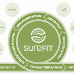
sureCore, with design centers in Sheffield, England, and Leuven, Belgium delivers custom low power design services. They do this down to the latest design nodes (7nm) and have specific experience in network, machine learning/AI, and IoT devices (e.g., medical, wearables, etc.). sureCore will be discussing their service engagement methodology and the unique mix of technology expertise at a SemiWiki Webinar Series event on Wednesday, August 28, 2019, from 10:00a m to 10:45 am PDT. To sign up for the webinar, register using your work email address HERE. We did a run through of the presentation last week and it is worth 20 minutes of your time, absolutely.
The breadth of sureCores’s experience cannot be overstated as they have handled all types of mixed-signal designs including ADC, DAC, amplifiers, regulators, PLLs, oscillators, etc. over process nodes ranging from 180nm down to today’s latest and greatest nodes. They have built their own proprietary automated design environment around proven industry tools from Cadence, Mentor, and Solido. Being an expert at Solido Varation Designer is a key skill/expertise in these types of designs. I know sureCore from my time at Solido Design Automation. They were one of many happy Solido customers, absolutely.
It is generally understood that most modern designs have a large portion of the layout area dedicated to memory, specifically SRAM. Any memory power savings gets multiplied due to the size of the memory. sureCore’s sureFIT custom memory design service gives its clients delivers memory instances specifically tuned to the needs of the application. At the webinar, they will be discussing an example of a custom-built, high capacity low power SRAM which delivered more than a 40% power savings compared to the typical memory compiler options available to their customer. You should attend the webinar to hear more about this example.
Beyond design services, sureCore also offers two other services, characterization, and verification. sureCore’s characterization solution is built using the Cadence Liberate tool suite. They characterize both SRAMs and standard cell libraries. The results include the generation of a .lib file for modeling across extreme PVT corners. As their focus is lower power design, they emphasize characterization at low operating voltages and support all the necessary views (NLDM, CCS (timing and noise), and LVF. The resulting models are validated using Monte-Carlo simulation on extracted netlists with the margins adjusted for improved design robustness.
Getting back to my original point, success in producing robust designs that meet the challenges of today’s low power specification does not require ‘art’; it requires science, experience, and expertise – and lots of it. sureCore’s low power design team has more than 200 person-years of combined lower power design experience. They have proven design experience down to 7nm, including custom SRAMs, layout, characterization, and more. Learn more about sureCore at their upcoming webinar.
About sureCore
sureCore Limited is an SRAM IP company based in Sheffield, UK, developing low power memories for current and next-generation, silicon process technologies. Its award-winning, world-leading, low power SRAM design is process independent and variability tolerant, making it suitable for a wide range of technology nodes. This IP helps SoC developers meet challenging power budgets and manufacturability constraints posed by leading-edge process nodes.
Also Read:
WEBINAR: The Brave New World of Customized Memory
Low Power SRAM Complier and Characterization Enable IoT Applications


