RVN! 26 Banner revised (800 x 100 px) (600 x 100 px)

Arm Mobility and Industrial Advances in Safety, Flexibility

Arm Mobility and Industrial Advances in Safety, Flexibility
by Bernard Murphy on 10-08-2020 at 6:00 am

Arm Pushes Mobility, Industry

Again on the theme of rationalizing NVIDIA’s $40B acquisition of Arm, two more hot areas for growth are mobility and industrial automation markets. NVIDIA is already strong in intelligent mobility and Arm is is virtually everywhere in the modern car. Ditto for robotics in industry. In fact the two domains have significant overlap: in sensing, sensor fusion, intelligent decision-making, path planning and need for safety, in many cases within a constrained power envelope. We’ve been enjoying a gold-rush of innovation, but consolidation is inevitable. Markets are ripe for off-the-shelf chip solutions. NVIDIA and Arm cloud and communication solutions. Add to that NVIDIA and Arm mobility and industrial solutions. Mmm.

Arm recently announced their next round of products supporting these autonomous systems, new CPU, GPU and ISP platforms. Cortex-A78AE is the automotive enhanced (AE) spin of the 64-bit v8.2 A78, Mali-G78AE and Mali-C71AE are the AE versions of Mali-G78 and Mali-C71 respectively. In each case, while ‘AE’ implies only automotive applications Chet Babla (Arm VP of Automotive and IoT) stressed that design for these platforms leverages learning from industrial and automotive input.

Cortex-A78AE for autonomy

The CPU core offers what Arm call Split-Lock mode, also offered in the earlier Cortex-A76AE core. In split mode, all cores in the cluster are available to operate independently, offering maximum throughput at modest safety levels. Lock mode is for tough ASIL-D (automotive ISO 26262) or SIL-3 (industrial IEC 61508) demands in which pairs of core operate in lockstep, trading off maximum throughput for safety. In split mode, the cluster can still rise to ASIL-B/SIL-2 certification if each core cycles periodically through diagnostic testing. This is a strategy I’ve mentioned before for chips which must pass ASIL-D even though subcomponents don’t all rise to that level. For earlier AE cores, shared logic in the cluster (DSU) also needed to be tested periodically. During those windows, all cores would be unavailable.

Cortex-A76AE offers a hybrid mode which for split mode operation offers lockstep support for the DSU, eliminating diagnostic impact from the DSU on throughput in ASIL-B/SIL-2 operation.

Mali-A78AE for autonomy

Arm tout Mali-A76AE as their first GPU to support safety requirements, up to ASIL-B/SIL-2. Also relevant to safety, the GPU now supports up to 4 fully independent partitions. It already supported virtualized workloads, but this goes a step further. Sure the GPU can run multiple workloads virtualized, but some of those loads may now be safety-critical. Which demands a higher level of separation than a virtual barrier, something a partition can provide. Partitioning doesn’t remove support for virtualization. This is still possible within a partition, say for non-critical loads like infotainment.

Mali-C71AE for autonomy

Arm first launched their Mali-C71 ISP core in 2017. As a fairly new entrant in this field, at least visibly (ha-ha), you’d think they have a lot of catching up to do. But they’ve been at this for a long time, working with companies like Nikon, Sony, Samsung and HiSilicon. As an example, their Iridix technology for HDR (high dynamic range) management is pretty impressive. Now the IP supports up to 4 real-time cameras (or 16 buffered cameras) with up to 1.2 Gigapixel/second throughput. And in this AE version, they have added safety support to cover up to ASIL-B/SIL-2 levels. Vey necessary for vision at the edge.

Back to the future

Chet wrapped up with a big statement. He believes autonomy will be the predominant workload of the future, between I assume different flavors of mobility and robotics. Early in the announcement he said that Arm estimates autonomy will represent an $8B silicon opportunity by 2030. In the Q&A he was asked how that split between automotive and industrial. Chet acknowledged that a large proportion would go to automotive. However he said that the industrial opportunity is still quite nascent. In the $8B number he’s extrapolating conservatively. Based on the engagements they already have he sees a very big opportunity for growth. Maybe yet another reason for that $40B price tag. (Whither Mali? Maybe low-power/edge applications, NVIDIA as the center of the web?).

For more details, click here.


Apple Is Evaluating Scratch Resistant Diamond Like Coatings On Gorilla Glass

Apple Is Evaluating Scratch Resistant Diamond Like Coatings On Gorilla Glass
by Robert Castellano on 10-07-2020 at 10:00 am

DLC T1

Despite the improvements in glass material used in smartphone displays, many, if not all, leading smartphone manufactures such as Apple  and other smartphone manufacturers are evaluating a coating method that further increases the durability of screens at a cost of just pennies per display by coating them with diamonds.

Gorilla Glass

Corning introduced Gorilla Glass Victus on July 22, 2020, and it’s the seventh generation of Gorilla Glass. It replaces Gorilla Glass 6, which was introduced in 2018. In lab tests, Gorilla Glass Victus achieved drop performance up to 2 meters when dropped onto hard, rough surfaces. Competitive aluminosilicate glasses from other manufacturers typically fail when dropped from less than 0.8 meters, according to Corning. Gorilla Glass Victus also surpasses last year’s Corning Gorilla Glass 6 with up to a 2x improvement in scratch resistance. Additionally, the scratch resistance of Gorilla Glass Victus is up to 4x better than competitive aluminosilicate glasses.

Scratching the phone makes it much more vulnerable to breaks. according to a study in November 2018 by Allstate subsidiary SquareTrade. Cracked screens were the most common form of damage, accounting for 29% of damaged smartphones, followed by scratched screens (27%) and nonworking batteries (22%).

Dropping a phone on the ground was the culprit in 74% of these cases. American smartphone owners broke more than 50 million screens in 2017 — nearly two every second — and spent $3.4 billion to replace them. On average though, those repairs cost from $170, and for the iPhone Xs Max, that figure goes up to a staggering $329.

A total of $14 billion repairing and replacing iPhones since their debut in 2007. The survey also showed that iPhone users were six times more likely to damage their phones than lose them or have them stolen.

Two-thirds of consumers said they wouldn’t repair a damaged phone if it still worked, while 59% said they would upgrade their device rather than fix an old one.

Diamond Like Coatings

Diamond-like coatings (DLC) are used in numerous applications because of unique properties such as low friction, high hardness, and high corrosion resistance.

In addition, DLC coatings possess both high thermal conductivity and electrical resistivity. The combination of these properties is useful for applications in microelectronics, medical devices, and automotive components.

DLC coatings can be used as protective coatings on displays, sensors and flexible semiconductors, where they greatly increase durability and can extend the total life of the final product. In this article I want address the demand for DLC for displays, in light of interest by Apple and other smartphone manufacturers to keep the display glass from damage.

Background

Diamond-like carbon first appeared in the Journal of Applied Physics in 1971 entitled “Ion-Beam Deposition of Thin Films of Diamondlike Carbon.” A year later, my team at Bell Labs in Murray Hill, NJ used a penning ion beam source to bombard a graphite block to deposit DLC on a substrate. The ion beam was comprised of argon ions.

The technology took a giant leap forward when my friend, Christian Weismantel, a scientist at Karl Mark Stadt, substituted carbon-containing methane for argon as the excitation gas in 1978.

Then in 1984, Air Products and Chemicals Inc.  developed technologies for producing synthetic diamonds. In 1990, “Diamonex” became an independent company after being spun off from APD.

Diamonex won a $10 contract over Morgan Crucible Co. to supply parts for the B-1 bomber, a British company. To get even, Morgan purchased Diamonex in 2001. My neighbor, David Hoover, a founder of the company, became CEO. My son plays poker with his son.

Deposition Methods

The methods for producing DLC films are broadly divided into two types: Physical Vapor Deposition (PVD) and Chemical Vapor Deposition (CVD). The PVD method uses a solid (graphite) as the carbon source and the CVD method uses a gas (a hydrocarbon such as methane). The PVD method is further divided into the arc, sputter, and laser vapor deposition methods.

The CVD method includes radio-frequency (RF), direct- current (DC) discharge, Penning ionization gauge (PIG), and self-discharge methods.

Deposition Equipment Market and Analysis

There are two suppliers of deposition equipment in this space: Intevac, which uses a sputtering technology, and privately held Denton Vacuum (Moorestown, NJ), which has developed several equipment configurations including sputtering and plasma-enhanced chemical vapor deposition (PE-CVD) that can be integrate with an ion source for ion assisted deposition or pre-clean. An analysis of these products and capabilities will be discussed in this article.

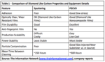
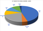
Table 1 presents an analysis of DLC films and equipment according to The Information Network’s report entitled “OLED and LCD Markets: Technology, Directions and Market Analysis.”

Table 1 compares the DLC properties and equipment for the three equipment manufacturers discussed above. There are two considerations:

  • The film composition and raw materials
  • The type and manufacturer of equipment

The Intevac films are diamond like carbon while the Denton Vacuum film is a diamond like nanocomposite materials. The latter may give rise to better film properties such as excellent film durability, anti-fingerprint capability, and low-cost scalability.

On the equipment side, we need to go to the origin of the technology. Intevac modified its Lean 200 Platform they used for sputtering DLC on HDD platers, limiting tool so they have to coat individual phone screens to just two displays.

Denton Vacuum’s DLC systems are not modified, but expandable for various substrate sizes, such as Gen 3.5 or Gen 6 display motherglass:

  • The Voyager is a plasma-enhanced chemical vapor deposition (PE-CVD) system with a focus on diamond-like carbon (DLC) that can coat planar (ex. silicon wafers), and three-dimensional parts (ex. optical lenses). In addition, there is an optional proprietary chamber configuration to enable co-sputtering of metals during DLC deposition for metal doped DLC (Me-DLC) films. For the greatest process flexibility, a patented Denton ion source can be integrated for ion assisted deposition or pre-clean.
  • The Phoenix in-line system offers high throughput for large volume production, and supports both planar and 3D component processing. This thin film deposition system can accommodate RF, AC, DC and pulsed DC sputtering as well as PE-CVD processes, and substrates or pallets up to GEN 3.5 glass size (600mm X 720mm).

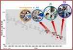
Table 2 shows unit shipments and forecasts for smartphones, which are the target markets for DLC. Shipments are expected to grow from1,508 million units in 2017 to 1,721 million in 2023. There are several important facts of this table, according to The Information Network’s report entitled “Hot ICs: A Market Analysis of Artificial Intelligence, 5G, CMOS Image Sensors, and Memory Chips.”

5G smartphones will be growing at about 50% per year once Apple enters the market sometime in late 2020.

OLED displays are replacing LCD displays. The crossover in shipments is expected to o.ccur in 2020, with about 850 million units of each type will be sold

Flexible OLED displays are replacing rigid displays. The crossover should occur in 2020 when about 350 million units of each type will be sold. Charts 1 and 2 illustrate the transition from rigid to flexible displays and the small growth of foldable smartphones.

Foldable phones will exhibit slow penetration through 2023 due to high prices and durability issues.

Chart 1

Chart 2

Table 3 shows that both rigid and flexible OLED displays use Gorilla Glass (or an aluminosilicate substitute), as well as comparing construction properties of both.

DLC Equipment Market

In Intevac’s September 1, 2020 Investor presentation, the company estimated that with $200M in sales over 5 years, a 10% to 15% penetration can be achieved (slide 16). That is based on the performance of Intevac detailed in Table 1 based on a mean time between cleaning of 250 hours, Most importantly, it is based on throughput of the system – the ability to coat two displays at one time.

My analysis using data from Denton Vacuum is shown in Table 4. It is based on a model of achieving 21% penetration in year 1 growing to 57% in 2024. This model is for displays using Gen 6 Glass (1500mm x 1850mm), coating 250 5.8” displays/motherboard at one time, and a throughput of 1 motherglass per minute for the deposition of the DLC. I compare smartphone penetration for the same $200 million equipment spend between 2020 and 2024.

Synopsis

Corning recently introduced its 7thgeneration of Gorilla Glass, a chemically strengthened glass designed to be thin, light and damage-resistant. Despite improvements with each generation, glass is still susceptible to scratches, which weakens it and makes it vulnerable to breakage. In 2017, 50 million smartphone displays were broken resulting in replacement costs of $3.4 billion. Since Samsung and Apple use Gorilla Glass in their smartphones, it’s obvious a high percentage of these 50 million displays were protected with Gorilla Glass, probably Gen 6.

Three deposition companies have developed systems to coat glass, Gorilla Glass or other aluminosilicate glasses with diamond like coatings with unique properties such as low friction, high hardness, and high corrosion resistance. Intevac, a public company, has modified its HDD deposition system to coat display glass with DLC. Denton Vacuum, which has been in the equipment business for 50 years, has developed two systems for DLC, offers them at competitive prices than competitors, and achieves better film characteristics, especially durability.

Intevac’s DLC system can reach 15% penetration of smartphones over a five year period with a spend of $200 million. The Denton Vacuum DLC system can achieve a 57% display penetration in the same period for the same $200 million spend.


Digital Design Technology Symposium!

Digital Design Technology Symposium!
by Daniel Nenni on 10-07-2020 at 6:00 am

Synopsys Digital Design Symposium 2020
Virtual events are coming fast and furious. Even though we are sheltering there is still the need to pick and choose carefully because time really is big money inside the semiconductor design ecosystem, absolutely. 

Synopsys virtual events are high on my list for three reasons:

  1. They are very well organized and professionally done
  2. Great customer driven content
  3. Who knows more about design and IP than the #1 EDA and #1 IP company?

Next up is the Synopsys Digital Design Symposium on October 14. Even though I do miss the networking and great food at Synopsys live events, I really am enjoying watching these events from my La-Z-Boy command center. Not to mention the ability to hit pause and rewind for better blogging.

REGISTER HERE

Digital Design Technology Symposium

HPC, 5G, mobile, automotive, AI: these are the technology segments that are bringing new design challenges to ASIC and SoC designers. For the past two years, Synopsys has been hard at work delivering a continuous stream of innovative products with future-proof technologies to address ultra-low power design, exploding design sizes and signoff scenarios, functional safety, security, and yield optimization. The Digital Design Technology Symposium is an event that showcases Synopsys’ digital design solutions.

With something of interest for a broad range of market segments, drop in and see how Synopsys’ innovative solutions can help with your next design. Whether you are targeting improved power, performance and area, yield, time-to-market or all of the above, recent advances in Synopsys’ Fusion Design Platform solutions can help you meet your digital design goals. You will gain new insights from Synopsys R&D experts, users, and partners on integrated, end-to-end solutions being used to achieve industry leading QoR and productivity in key areas.

Who Should Attend?

Digital design managers/directors, and engineers working on their next SoC or ASIC. Especially those challenged by requirements in the HPC, 5G, mobile, automotive, and AI market segments.  CAD managers/directors looking to integrate the latest design innovations into their in-house design flows to boost design team productivity and improve design quality. Senior level engineering management wanting to understand where Synopsys is headed and why they should invest long term in Synopsys design solutions.


Keynotes Spotlight

Wednesday, October 14, 2020

Running with the Bulls: Synopsys Innovations to Address the Next Wave of Design Challenges

Wednesday, October 14 | 9:00 AM PDT

With semiconductors fueling much of the ”Smart Everything” revolution, EDA has been front-and-center in the spotlight as a key enabler for continuing density, performance and performance-per-watt improvements. The challenges faced by advanced node designers include timely enablement, full-flow throughput, end-to-end power optimization and multi-die integration to name a few. In addition, AI hardware accelerators are driving strong interest in domain specific architectures and the need for rapid RTL exploration with accurate power, performance and area  (PPA) measurements. Looking ahead, AI/ML and Cloud open up several new innovations in the EDA space to optimize and accelerate EDA flows. With functional safety, reliability and security concerns paramount in mission-critical applications, design flows need to natively represent these careabouts without compromising design PPA goals. In his presentation, Shankar will review the latest innovations in Synopsys’ Fusion Design Platform to address these challenges and opportunities.

Shankar Krishnamoorthy
Sr. VP Engineering
Synopsys
Sriram Satakopan
VP Engineering
NXP Semiconductors

Cost, Differentiation and Time-to-Market: How Hyperconvergence in EDA is Helping Solve Key Business Growth Imperatives

Wednesday, October 14 | 9:25 AM PDT

To execute successfully in critical market segments such as automotive, industrial & IoT, mobile and communications infrastructure requires a laser focus on differentiation, cost and time to market. Increasing complexity as the transition is made to advanced process nodes requires a redefinition of the SoC development flow to substantially lower project cycle times and increase engineering efficiency. Parallel execution is critical to meeting 10-week cycle times and addressing the challenges faced with a 6x increase in instances per square millimeter. Many metrics of engineering efficiency need to be monitored and improved as design complexity increases and fewer engineering resources are available. These challenges are driving the need for a highly convergent, vertically integrated digital design solution that delivers predictable quality of results together with faster turnaround times. Learn more about the SoC design challenges being faced and how these are being addressed today.

About Synopsys

Synopsys, Inc. (Nasdaq: SNPS) is the Silicon to Software partner for innovative companies developing the electronic products and software applications we rely on every day. As the world’s 15th largest software company, Synopsys has a long history of being a global leader in electronic design automation (EDA) and semiconductor IP and is also growing its leadership in software security and quality solutions. Whether you’re a system-on-chip (SoC) designer creating advanced semiconductors, or a software developer writing applications that require the highest security and quality, Synopsys has the solutions needed to deliver innovative, high-quality, secure products. Learn more at www.synopsys.com.

Also Read:

Netlist CDC. Why You Need it and How You do it.

The Big Three Weigh in on Emulation Best Practices

Synopsys Presents SAT-Sweeping Enhancements for Logic Synthesis


Webinar: Addressing the Challenges of Hyper-scaling within Data Centers with Advanced Node Embedded Sensing Fabrics

Webinar: Addressing the Challenges of Hyper-scaling within Data Centers with Advanced Node Embedded Sensing Fabrics
by Mike Gianfagna on 10-06-2020 at 10:00 am

Webinar Reminder Image

I had a chance to preview the subject webinar recently.  Yes, it’s a long title, but a very important topic. When it comes to hyper-scale data centers, there are substantial challenges associate with thermal management, power distribution and processing performance. Moortec explores approaches to these issues using their real-time embedded sensing fabrics. Benefits of this technology include enhanced reliability of operation as well as dynamic power and speed optimization. Advanced node embedded sensing fabrics are definitely worth a close look.

The webinar is kicked off and closed by Ramsay Allen, marketing manager at Moortec. Richard McPartland, technical marketing manager at Moortec, presents the bulk of the material. Richard has a long history as a product manager within the semiconductor industry. He begins the webinar by pointing out that the energy consumption for data centers today is 1-2 percent of all global electricity consumption. These numbers will go up over time, so this is clearly an area for optimization and power reduction. Richard provides a good overview of the macro trends associated with data center power consumption. You get what you measure essentially.

Richard then catalogs power challenges along three categories – thermal management, IR drops and process variation. He further analyzes the constituent parts of a large data center campus. Wonder how many semiconductor devices there are in such campus?  You’ll need to watch the webinar to find out.

Everyone knows voltage is a fundamental contributor to power consumption. Tightly control and lower the voltage and power consumption goes down. The control part requires sensing of the actual delivered voltage at critical circuits on the chip.  Here is where Moortec sensing technology starts to make a difference. When you apply small savings against the previously mentioned macro models of data center campuses, big things happen. It tuns out enhanced thermal management through distributed sensing is an excellent approach to power management.

Richard points out that advanced process nodes deliver higher logic density, and the distributed sensing approach discussed is quite effective here. The high accuracy of Moortec sensors also contributes to management of power, heat and improved performance as well. How does all this fit together?  You will need to watch the webinar to find out. I can say the results are significant and will surprise you.

The long-term benefits of precision monitoring also translates into better system reliability and uptime. This has to do with enhanced system management and predictive analytics. Richard points out that Moortec provides comprehensive, sub-system level capabilities from 40nm to 5nm. Note I covered Moortec’s distributed, real-time thermal sensing on TSMC N5 here. These capabilities deliver a fabric that can monitor thermal conditions real-time throughout the chip, along with voltage levels as well as process monitors that can determine the capabilities of each chip for individual optimization. Richard concludes with a roadmap discussion of what the future holds. You definitely need to watch this part.

The Moortec webinar, Addressing the Challenges of Hyper-scaling within Data Centers with Advanced Node Embedded Sensing Fabrics will be broadcast on Tuesday, October 13, 2020 at 10AM Pacific time. You can register for the webinar here.


Arm Neoverse. Central to NVIDIA Strategy?

Arm Neoverse. Central to NVIDIA Strategy?
by Bernard Murphy on 10-06-2020 at 6:00 am

Arm Neoverse

I’ve covered Arm Neoverse updates a few times already, a span of products with application from the cloud through infrastructure to the edge. Logical strategy of course but Arm has been delivering some impressive wins suggesting this is more than just a loose marketing concept. Overlap with NVIDIA in datacenters and supercomputing are also suggestive. Arm strength in communication infrastructure, particularly in 5G potential, is another hint. All driven by systems houses who are getting into chip design because they have to, rather than necessarily want to. Lots of new technology in high value, high margin designs which as chips could justify NVIDIA’s $40B investment. Maybe Arm also continues the IP business but the real money is going to come from chips leveraging Neoverse tech and NVIDIA GPU/AI tech for these markets. I should stress that this is purely my speculation.

Arm Neoverse progress in the cloud

Chris Bergey, Sr. VP and GM of Infrastructure at Arm (a recent acquisition, previously a Sr. VP at Western Digital) announced the 2020 lineup for Neoverse. He reminded us that there have already been public announcements from 4 of the top 7 hyperscalers about Arm-based server deployments. They continue to encourage cloud-related software ecosystem support through capabilities like Docker and Kubernetes and he referenced work Microsoft has been doing on Open JDK and Amazon has been doing on PHP. All of this folding Arm more and more tightly into the cloud.

V, N and E series processors

When Arm launched Neoverse in 2018 they talked about a roadmap for a series of platforms. In 2019 they refined the structure to an N1 platform for cloud/infrastructure and E1 platform for the edge (the boundaries are a bit fuzzy). AWS built their Graviton processor on N1, introducing the A1 instance to the EC2 menu of compute options. Chris acknowledged that while they talked about a power-performance message in positioning these instances, it didn’t resonate strongly since servers aren’t battery-powered (I wondered too).

Now they’ve refined their story. An N series platform balances performance, area and power, as before. An E series platform prioritizes area and power over performance (for the edge). Now Arm are introducing a V series (previously Zeus) with scalable vector extensions (SVE) which puts performance first, allowing for some compromise in area and power. This can deliver approaching a 2X performance uplift over N1, allowing the silicon partner some level of implementation control. It also supports CCIX for cache coherence across die/packages. Since Fujitsu/Fugaku is one of the quoted references on this topic, I’m guessing they depended on that capability. So the V series now directly addresses that earlier datacenter performance concern. For applications that still need power-performance efficiency, later this year they will introduce an N2 platform with 40% higher per-thread performance to further enhance scale-out support.

Arm Neoverse in communication infrastructure

Back to my speculation. A major trend in infrastructure outside the datacenter is to Open-RAN. Network operators desperately need more efficient and cost-competitive solutions over traditional RAN architectures, especially as 5G demand grows. Which is why they are pushing open standards very hard. The default hardware support in many cases is big GP-CPUs and FPGAs, both expensive. Operators are looking for more flexible and competitive solutions to populate central and distributed units and gateways/small cells. Right now, there’s a shortage of chips to drive this development. That seems like a pretty compelling opportunity for NVIDIA+Arm.

You can read the announcement HERE.


EDA Appears to Have COVID Immunity – ESD Alliance Reports Strong Q2 2020

EDA Appears to Have COVID Immunity – ESD Alliance Reports Strong Q2 2020
by Daniel Nenni on 10-05-2020 at 10:00 am

EDA Appears to Have COVID Immunity – ESD Alliance Reports Strong Q2 2020

The ESD Alliance tracks revenue growth for a large number of EDA companies. Their recent report paints a positive picture in a landscape dotted with challenges and not-so-good news. The report cites 12.6% overall revenue growth for Q2 2020 vs. Q2 2019. Furthermore, the overall most recent four quarter revenue average has increased 6.7% when compared to the prior four quarters. It’s all up and to the right. Employment in EDA paints a similar picture, with a 5% increase in headcount for Q2 2020 vs. Q2 2019 and a 1.4% increase for Q2 2020 vs. Q1 2020.

“EDA is a pretty good place to be” Wally Rhines

Mike Gianfagna I got the opportunity to speak with Wally Rhines about the report to get his perspective and try to understand the story behind the numbers. Wally wears many hats, in the context of this discussion he is the executive sponsor for the SEMI EDA Market Statistics Service. First, we discussed revenue by category for Q2 2020:

  • CAE revenue increased 16.1% to $922 million compared to Q2 2019. The four-quarter CAE moving average increased 7.1%
  • IC Physical Design and Verification revenue increased 16.8% to $584.1 million compared to Q2 2019. The four-quarter moving average for the category rose 4.8%
  • Printed Circuit Board and Multi-Chip Module (PCB and MCM) revenue decreased 0.3% to $243.5 million compared to Q2 2019. The four-quarter moving average for PCB and MCM increased 12.4%
  • SIP revenue increased 13.6% to $948.2 million compared to Q2 2019. The four-quarter SIP moving average grew 8.5%
  • Services revenue decreased 12.8% to $86.2 million compared to Q2 2019. The four-quarter Services moving average decreased 14.3%

Two things jumped out for us here. First, why the poor showing for PCB and MCM. Wally pointed out that while the Q2 2020 vs. Q2 2019 data was low, PCB is still on track to deliver a stellar growth year overall. Regarding services, the bad performance is a bit of a mystery. Wally offered on his personal opinion on this one. He pointed out that when times get tough, outsourced services are brought in house. This could be one of the few negative impacts COVID may have on EDA.

He also pointed out that a lot of services work is done on-site, and COVID has definitely slowed down on-site work. Wally also provided a bit of color on the strong semiconductor IP (SIP) growth. All categories are up except ethernet and DDR controllers, which are flat.

Looking at revenue by region:

  • The Americas, the largest reporting region by revenue, purchased $1,155.6 million of EDA products and services in Q2 2020, an 11.4% increase compared to Q2 2019. The four-quarter moving average for the Americas increased 4.6%.
  • Europe, the Middle East, and Africa (EMEA) revenue increased 5.2%, to $377.5 million compared to Q2 2019. The four-quarter moving average for EMEA grew 12.2%.
  • Japan revenue increased 9% to $240.4 million compared to Q2 2019. The four-quarter moving average for Japan rose 0.8%.
  • APAC revenue increased 18.1% to $1,010.3 million compared to Q2 2019. The four-quarter moving average for APAC increased 6.3%.

We felt that lumping several key regions into one APAC number didn’t really tell the whole story. I typically find that Wally has data at his fingertips for almost everything. He didn’t let me down this time. Here is the breakout for APAC (Q2 2020 vs. Q2 2019):

  • China: 36.4%
  • India: 16.8%
  • Korea: 0%
  • Taiwan: 25%
  • Rest of Asia: 32%

True to form, we chatted about a few other related topics during our meeting and Wally had more insightful data at his fingertips. Regarding venture funding for EDA, approximately $2B was invested in 2019 and it looks like the total investment for 2020 will be similar. The makeup changes, however. In 2019, investments were roughly split 50/50 between the US and China. In 2020, China plays a much larger role.

We also talked about the exploding server market. The growth here is fueled in large part by all the data analytics needed, thanks to the deluge of information from our connected world. Wally left us with an interesting observation. Companies like GE and Pratt & Whitney collect about 70 terabytes of data per hour for every jet engine that is in the air. That massive amount of data is then analyzed to spot potential operational issues and to develop maintenance schedules that are tuned to the actual equipment.

These companies are the only ones who can offer this service for their products and the customer is absolutely dependent on it for safety and smooth operation. It brings up the question of whether jet engine manufacturers should simply give the engines away for free in exchange for long-term data analysis contracts.

I also spoke to Eric Esteve of IP Nest about the SIP market:

“Design IP growth rate is impressive, year after year since 2010. The four-quarter moving average growth of 8.5% confirms the fact that Design IP category is growing more than the semiconductor (excluding memory), as IPnest has shown since monitoring this market. It will be interesting to check if Interface IP category yearly growth in 2020 will be as in 2019, or +18%.”

ESD Alliance Reports Strong Electronic Design Automation Industry
Revenue Growth for Q2 2020


SMIC China Sanctions – Headwinds For Applied Materials And Lam Research

SMIC China Sanctions – Headwinds For Applied Materials And Lam Research
by Robert Castellano on 10-05-2020 at 6:00 am

Micron Technology and SMIC C1

On September 26 there were media reports that the U.S. Commerce Department has added China’s largest chipmaker, Semiconductor Manufacturing International Corporation (SMIC) , to its entity list, after it determined there an “unacceptable risk” that equipment SMIC received could be used for military purposes

U.S. firms would now need a license to export certain products to China’s largest chipmaker because of an “unacceptable risk” that the goods could be used for military purposes.

So far the SMIC news is unsubstantiated, but news of pending restrictions on September 5 was a catalyst for SMIC’s stock dropping 25% on the news.

SMIC reiterates that it manufactures semiconductors and provides services solely for civilian and commercial end-users and end-uses. The Company has no relationship with the Chinese military and does not manufacture for any military end-users or end-uses.

The largest customer of SMIC is Huawei (18.7% of sales), followed by Qualcomm  (8.6%), Broadcom (7.5%), ON Semi (3.5%), Cobo (2%), and Cypress (1.2%).

The three major equipment suppliers that SMIC purchases are ASML, Lam Research, and KLA, which are estimated to account for 11%, 6.6%, and 3.5% of SMIC Capex, respectively.

Most important, SMIC dominates the 12-inch capacity of IC companies in China with 45% of capacity in 2019, as shown in Chart 1. A loss of SMIC will make a huge dent on sales of semi cap equipment.

Table 1 shows that SMIC had planned on increasing its capex spend 258.3% in 2020.

SMIC has a 12-inch fab in Shanghai, and semiconductor imports into Shanghai province totaled $2,450 million in 2020. In addition to SMIC, Shanghai province is also home to 300mm Huali and Hua Hong Grace, so not all equipment was imported by SMIC. But referring back to Chart 1, SMIC has a 45% share of capacity compared to 21% for Huali and 5% for Hua Hong. In addition, SMIC’s capex spend represented 81% of the total of $8.3 billion in 2020. So for all intents and purposes, most of the equipment imports in Table 2 went to SMIC.

So, SMIC and Shanghai peers have been on a buying spree in anticipation of U.S. Government embargo of equipment into the country. Table 3 shows the SN1 plant capacity, that will reach 70,000 wspm when fully furnished.

Most important, SMIC has a dominant posture in advanced nodes. As I said in my above-mentioned article, SMIC held revenues of $12 million in 14nm chips in Q1 2020. While it represented just 1.3% of revenues, it was expected to grow.

Also, SMIC has been able to move beyond 14nm without the quantum step to move directly to 7nm. SMIC’s N+1 process has entered the stage of customer introduction and product certification. Compared with the 14nm performance, the N+1 process has a 20% improvement in power consumption, a 57% reduction in power consumption, a 63% reduction in logic area, and a 55% reduction in SoC area, which is close to TSMC’s 7nm process.

Thus, the remaining capex spend in 2020 and the forecasted $3,200 million in 2021 would have been earmarked on advanced nodes, and not for capacity expansion for mature nodes.


Will the U.S. and China go to War for TSMC?

Will the U.S. and China go to War for TSMC?
by Daniel Nenni on 10-05-2020 at 4:00 am

Will the U.S. and China go to War over TSMC

The semiconductor industry has never been more exciting than it is today and that is a mouthful given what we have accomplished over the last 50 years. From mainframe computers to a supercomputer in our pockets or on our wrists. Even if you don’t believe in miracles, semiconductor technology comes really close, absolutely.

U.S. tightens exports to China’s chipmaker SMIC, citing risk of military use REUTERS

When I started my career 36 years ago you would be hard pressed to find a person who had heard of a semiconductor much less knew what one really was. Today, it is still hard to find people who really know semiconductor design and manufacture (especially in the media) even though you can read about it every day, especially now that semiconductors could lead to the next world war.

Before you write me off as another click-baiting-chicken-little think about how important semiconductors are to modern life. Not just important, semiconductors are critical to modern life. Not just critical, semiconductors could mean the difference between life and death.

Disagree? Imagine our world without electronic devices. Imagine a business or hospital without digital equipment. Imagine a military without high tech gear. Are you getting the picture? Life or death.

Now understand that semiconductors are where modern electronics begin and end for that matter. Also understand that the semiconductor chip may have been invented in the United States but today it is a worldwide supply chain.

To be clear, no one country can succeed in semiconductor design and manufacture without others. Having grown up in Silicon Valley and spending the majority of my semiconductor professional life traveling the world I know this firsthand, front row seat, I lived it.

Being from a military family and a military history enthusiast I also know a little bit about war. My grandfather served in WWI as an Army medic and lived to tell about. In fact, he lived 102 years under my care so I heard all about it. My other Grandfather was at Pearl Harbor, my father served in Korea, and my Uncle in Vietnam. War is hell.

One of the strategic things to do when waging a war is to cut off their supply lines, right? Food, water, fuel, raw materials, etc… You can now add semiconductors to that supply list.

So why is the United States today cutting off the semiconductor supply line to China? It’s an act of war and if there is an actual war over semiconductors, where will it be fought?

Taiwan of course. Taiwan is the semiconductor manufacturing hub of the world. Taiwan is also the Republic of China, which is what my passport says, and even without semiconductors China wants political control over Taiwan. Something like what is happening in Hong Kong only with a full-on war declared.

Why is Taiwan so important to the semiconductor supply chain? Because Taiwan is the home of TSMC (Taiwan Semiconductor Corporation), the worldwide champion of semiconductor manufacturing. My first book “Fabless: The Transformation of the Semiconductor Industry” goes into more detail on how TSMC came about but the bottom line is; It’s all about the ecosystem (supply chain). Hundreds of companies around the world brought us to where we are today and nothing short of a war can stop the semiconductor ecosystem from succeeding.

Could it even be possible? China at war with the US through Taiwan? Ten years ago from the Lobby of Hotel Royal in Hsinchu I would have said absolutely not. Today, sheltering in Silicon Valley, given the current political instability and oncoming economic challenges, given the eye-for-an-eye +1 behavior of the US and China leadership, I say war is probable. Unless of course the world recognizes semiconductors as a matter of life or death and gets civilized around it. Just my semiconductor professional opinion of course.


Painful IoT Security Lessons Highlighted by a Digital Padlock

Painful IoT Security Lessons Highlighted by a Digital Padlock
by Matthew Rosenquist on 10-04-2020 at 10:00 am

Painful IoT Security Lessons Highlighted by a Digital Padlock

The first warning sign was “hackproof” in the 360Lock marketing materials. As it turns out, with no surprise to any security professional, the NFC and Bluetooth enabled padlock proved to be anything but secure.

Straightforward penetration testing revealed horrible logical and physical security for a padlock that promotes itself as “incorruptible” and “hackproof”!

Digital Transformation is a rush to connect our physical world to the global electronic ecosystem to enable better access, integration, and advanced capabilities. Internet of Things (IoT) devices are often at the forefront of this movement, turning normal devices into ‘smart’ devices. Sometimes even the best ideas fail when it comes to design and execution.

This padlock has several innovative features such as connectivity to mobile applications, an included RFID wristband and tag for easy unlocking, configurability to add access for others, and a detailed history log. What it lacks however, is actual security.

Security theater

Simple pentesting proved what was likely a foregone conclusion. The kickstarter funded lock is neither hackproof nor secure. Testers found that simple replay attacks could trick the logic to open the device. Additionally, crude brute-force methods were able to compromise the integrity of the lock mechanism. Pounding it with a hammer quickly defeated the padlock.

The results highlighted that the $40 lock is not robust and better served as a visual deterrent, casual locking device, or novelty item.

An industry problem

A massive quantity and vast diversity of smart devices are emerging. Most connect to the internet and require a high degree of security. Connectivity accentuates vulnerabilities. Sadly, many of the IoT devices consumers and businesses are embracing lack the necessary measure for security rigor, leaving users exposed and data vulnerable.

The 360Lock is not the only device that has poor security, but it does highlight two important points, emphasizing overall industry challenges.

First, never trust any product that claims to be ‘unhackable’. Seasoned security professionals would never make such an outlandish assertion as to say a device is hackproof! The fact that 360Lock promoted their product in this way was the only indicator needed to instill great skepticism.

Second, this device’s weaknesses highlight the need for proper data transport security. Man-in-the-Middle (MitM) attacks, such as a replay attacks, are common tactics for hackers. Transactional security is absolutely critical to protect data and requests. Unfortunately, securing data in-transit between IoT devices on the edge and phones/PC/cloud-services requires the right expertise and tools. Most failures occur in how data protections are implemented and managed. As a rule, if a product manufacturer is not detailing their security, they likely do not have quality capabilities in place.

Painful lessons

Consumers must be wary and realize that even dedicated security products, such as padlocks, can be victimized by poor development decisions. Trendy features are no replacement for solid security and reliability. IoT devices are often much less secure than the marketing materials and salesperson will reveal. Look for reputable manufacturers who have committed to work with the best technology, security integrators, and verification practices. Every consumer and business is responsible for understanding the risks accompanying the benefits of new technology.

Interested in more? Follow me on LinkedInMedium, and Twitter (@Matt_Rosenquist) to hear insights, rants, and what is going on in cybersecurity.


5G, Hyperscaling and the Resurgence of Consumer Silicon

5G, Hyperscaling and the Resurgence of Consumer Silicon
by Ramsay Allen on 10-04-2020 at 6:00 am

TSMC 5G OIP 2020

At the recent TSMC OIP Ecosystem Forum and Technology virtual events, TSMC re-affirmed their previous prediction that 5G is going to be a multi-year silicon mega-trend with the biggest drivers being the ramp up of 5G handsets, supporting infrastructure and the continued growth of high performance computing (HPC).

We all want the luxury of live streaming, whether it be a concert or sports event, playing the latest games or watching HD movies on our phone, but what is it that actually allows 5G ASIC designers to deliver this enhanced level of user experience? Today’s Semiconductor advanced node technology really is the beating heart of 5G network technology.  Powering network base stations, cars, smartphones, and other connected devices, but 5G also plays an integral part of a much bigger technology phenomenon…Hyperscaling.

5G infrastructure is extremely power hungry and generally requires ~3 times the number of base stations compared to older technologies such as LTE, due to the higher frequencies involved. Moortec is already working with customers in the 5G space to help address some of these infrastructure power issues.

5G Silicon Challenges

5G enabled devices such as handsets, tablets and wearables have certainly helped revitalize the consumer electronics space as they have moved from typically planar nodes down to FinFET process technologies like 5nm.

This step change does however present designers with specific challenges, one of the biggest being increased thermal activity associated with the data intensive workloads associated with the system​. Battery life can also be an issue when running 5G and associated applications like video, and gaming etc. If the thermal conditions are not carefully monitored and controlled, handsets may either switch to a lower power 4G mode or even turn off altogether. As a user why do I care? Well, apart from the handset becoming noticeably warmer to the touch, your video download will take longer or freeze and your phone will need recharging more frequently as the battery will drain faster.

A 5G small cell can be operational for over a decade in potentially hostile environments, without any forced air cooling and as such it is particularly important to be able monitor them remotely in the field.

Moore’s Law

In the last instalment of the Moortec ‘Talking Sense’ blog my colleague Tim Penhale-Jones talked about the impact that Moore’s law and Dennard Scaling have had on the advanced node semiconductor sector. For some time, we have been cramming ever increasing amounts of processing power into each 1mm2 of silicon and this has enabled the 5G technology that we see emerging today. However, the pressure continues to Miniaturize (device size), Maximise (power & performance) and Optimize (reliability & battery life) and in order to continue to do this successfully it is critically important to understand the dynamic conditions within the device itself.

Benefits of In-Chip Monitoring for 5G Devices

By implementing highly configurable, real time embedded sensing fabrics, chip designers can address some of the challenges associated with overheating, reduced data throughput and diminished battery life. This enhances the overall user experience in consumer products like 5G handsets and increases the performance optimization and reliability of infrastructure devices in the field.

To find out how Moortec’s in-chip monitoring technologies and sensing fabrics could benefit your next advanced node 5G project contact us today.

In case you missed any of Moortec’s previous “Talking Sense” blogs, you can catch up HERE.