Synopsys 800x100 px High Quality

Podcast EP50: Perforce at DAC

Podcast EP50: Perforce at DAC
by Daniel Nenni on 11-19-2021 at 10:00 am

Dan and Mike are joined by Simon Butler, general manager of the Methodics Business Unit at Perforce. Some history of DAC is discussed; what it’s like attending the show both as a small company and a larger one. The products Perforce will showcase at DAC this year are then discussed, The breadth of technology to support design infrastructure that Perforce brings to the industry is detailed by Simon.

The views, thoughts, and opinions expressed in these podcasts belong solely to the speaker, and not to the speaker’s employer, organization, committee or any other group or individual.

https://www.perforce.com/

https://www.dac.com/


2021 Semiconductors Finishing Strong with 2022 Moderating

2021 Semiconductors Finishing Strong with 2022 Moderating
by Bill Jewell on 11-19-2021 at 8:00 am

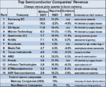
Top Semiconductor Comoany Reveue 2021

The semiconductor market in 3rd quarter 2021 was $144.8 billion, according to WSTS, up 7.4% from the prior quarter and up 27.6% from a year ago. The strong year-to-year growth was a slight deceleration from 30.4% in 2nd quarter 2021. The major memory companies reported very healthy 3Q21 revenue increases versus 2Q21 with all of them up double digits, led by Kioxia at 21.5%. Among the leading non-memory companies Qualcomm, AMD, Infineon, and NXP all had double digit growth. Intel was the only top semiconductor company with a revenue decline, down 2.2% in 3Q21 versus 2Q21.

The top semiconductor companies’ guidance for 4Q21 are mixed. Qualcomm expects 11.9% 4Q21 growth versus 3Q21 driven by strong handset growth, especially for Android smartphones. Nvidia, AMD, STMicroelectronics and NXP all project mid-single-digit revenue increases – citing datacenter, servers, gaming, automotive, and industrial as key drivers. Intel, Micron, MediaTek, Texas Instruments and Infineon all guided for 4Q21 revenue declines. The automotive market has drawn much attention for semiconductor shortages, however other markets are also showing problems. Weakness in the PC market due to shortages of some key components was highlighted as a concern by Intel, SK Hynix, Micron and Kioxia.

Constraints on supplies of semiconductors and other components are reflected in lower forecasts for the key end equipment categories of PCs and smartphones. In May 2021, IDC projected 2021 PC shipments of 357 million units, up 17.6% from 2020. In August 2021, IDC reduced its 2021 forecast to 347 million units, up 14.2% from 2020 and 10 million units lower than the May forecast. IDC cited supply chain issues for the lower forecast. Counterpoint Research in July 2021 expected 2021 smartphone shipments of 1,447 million units, up 8.7% from 2020. In September 2021, Counterpoint reduced its 2021 forecast to 1,414 million units, up 6.2% from 2020 and 33 million units lower than the July projection. Counterpoint blamed semiconductor shortages for its downward revision.

The most recent forecasts for the semiconductor market in 2021 and 2022 also incorporate the impact of supply constraints. Our November forecast from Semiconductor Intelligence calls for 2021 growth of 24.5% (down from 26% in our August forecast) and 14% growth in 2022 (down from 15% in August). IC Insights’ November projection of 23% growth in 2021 is down from their June forecast of 24.1%. Gartner is the most optimistic with an October estimate of a 27% increase in 2021. IDC has the lowest 2021 projection at 17%. With three quarters of data from WSTS and 4Q21 revenue guidance from most major companies, the 2021 semiconductor market will almost certainly finish in a range of 23% to 26%, the highest growth since 31.8% in 2010 following the great recession.

Our Semiconductor Intelligence forecast of 14% semiconductor market growth in 2022 is based on these key assumptions:

Normalization of growth of end equipment after higher-than-normal growth in 2021.

Relief of most major semiconductor and other component supply problems.

Continued recovery of most worldwide economies in 2022 following the worst of the pandemic.

The biggest uncertainty is the impact of COVID-19 in 2022. According to the Johns Hopkins University of Medicine, cases have risen over the last month following a decline from an August peak. Only 42% of the world’s population has been fully vaccinated, with the U.S. at 60%. Although most of the world has opened up, there are still numerous cases of local lockdowns. If COVID-19 is not mostly under control in 2022, the entire global economy will perform below its potential.

Also Read:

Semiconductor CapEx too strong?

Auto Semiconductor Shortage Worsens

Electronics Recovery Mixed


CEO Interview: Charbel Rizk of Oculi

CEO Interview: Charbel Rizk of Oculi
by Daniel Nenni on 11-19-2021 at 6:00 am

Charbel Rizk CEO Interview SemiWiki

Charbel Rizk is CEO of Oculi®, a spinout from Johns Hopkins University, a fabless semiconductor startup commercializing technology to address the high power and latency challenges of vision technology.  Dr. Rizk recognized these as barriers to effective AI in his years of experience as a Principal Systems Engineer, Lead Innovator, and Professor at Rockwell Aerospace, McDonnell Douglas, Boeing, JHUAPL and Johns Hopkins University. The Oculi vision solution reduces latency, bandwidth, and/or power consumption by up to 30x.

Why did you decide to create this technology?
Our original motivation was simply to enable more effective autonomy. Our perspective is that the planet needs the “human eye” in AI for energy efficiency and safety. Machines outperform humans in most tasks but human vision remains far superior despite technology advances. Cameras, being the predominant sensors for machine vision, have mega-pixels of resolution. Advanced processors can perform trillions of operations per second. With this combination, one would expect vision architecture (camera + computer) today to be on par with human vision. However, current technology is as much as ~40,000x behind, when looking at the combination of time and energy wasted in extracting the required information. There is a fundamental tradeoff between time and energy, and most solutions optimize one at the expense of the other. Just like biology, machine vision must generate the “best” actionable information very efficiently (in time and power consumption) from the available signal (photons).

What are the major problems with the current technology available in the market?
Cameras and processors operate very differently compared to the eye+brain combination, largely because they have been historically developed for different purposes. Cameras are for accurate communication and reproduction of a scene. Processors have evolved over time with certain applications in mind, with the primary performance measure being operations per second. The latest trend is domain specific architectures (i.e. custom chips), driven by demand from applications such as image processing.

Another important disconnect, albeit less obvious, is the architecture itself. When a solution is developed from existing components (i.e. off-the-self cameras and processors), it becomes difficult to integrate into a flexible solution and more importantly to dynamically optimize in real-time which is a key aspect of human vision.

As the world of automation grows exponentially and the demand for imaging sensors skyrockets, efficient (time and resources) vision technology becomes even more critical to safety (reducing latency) and to conserving energy.

What are the solutions proposed by Oculi?
Oculi has developed an integrated sensing and processing architecture for imaging or vision applications. Oculi patented technology is agnostic to both the sensing modality on the front end (linear, Geiger, DVS, infrared, depth or TOF) and the post-processing (CPU, GPU, AI Processors…) that follows.We have also demonstrated key IP in silicon that can materialize this architecture into commercial products within 12-18 months.

A processing platform that equals the brain is an important step in matching human perception, but it will not be sufficient to achieve human vision without “eye-like” sensors. In the world of vision technology, the eye represents the power and effectiveness of parallel edge processing and dynamic sensor optimization. The eye not only senses the light, it also performs a good bit of parallel processing and only transfers to the brain relevant information. It also receives feedback signals from the brain to dynamically adjust to changing conditions and/or objectives. Oculi has developed a novel vision architecture that deploys parallel processing and in-memory compute in the pixel (zero-distance between sensing and processing) that delivers up to 30x improvements in efficiency (time and/or energy).

The OCULI SPU™ (Sensing & Processing Unit), is a single chip complete vision solution delivering real-time Vision Intelligence (VI) at the edge with software-defined features and an output compatible with most computer vision ecosystems of tools and algorithms. Being fitted with the IntelliPixel™ technology, the OCULI SPU reduces bandwidth and external post-processing down to ~1% with zero loss of relevant information. The OCULI SPU S12, Our GEN 1 Go-To-Market product, is the industry’s first integrated neuromorphic (eye+brain) silicon deploying sparse sensing, parallel processing + memory, and dynamic optimization

It offers Efficient Vision Intelligence (VI) that is a prerequisite for effective Artificial Intelligence (AI) for edge applications.  OCULI SPU is the first single-chip vision solution on a standard CMOS process that delivers unparalleled selectivity, efficiency, and speed.

There is significant room for improvement in today’s products by simply optimizing the architecture, in particular the signal processing chain from capture to action, and human vision is a perfect example of what’s possible. At Oculi, we have developed a new architecture for computer and machine vision that promises efficiency on par with human vision but outperforms in speed.

Do you want to talk about the potential markets? R&D?
We have developed a healthy pipeline of customers/partners engagements over a variety of markets from industrial and intelligent transportation to consumers to automotive. Our initial focus is on edge applications for eye, gesture, and face tracking for interactive/smart display and AR/VR markets. These are near term market opportunities with high volume and Oculi technology offers a clear competitive edge. As biology and nature have been the inspiration for much of the technology innovations, developing imaging technology that mimics human vision in efficiency but outperforms in speed is a logical path. It is a low hanging fruit (performance versus price) as Oculi has successfully demonstrated in multiple paid pilot projects with large international customers. Also unlike photos and videos we collect for personal consumption, machine vision is not about pretty images and the most number of pixels.

Also Read:

CEO Update: Tuomas Hollman, Minima Processor CEO

CEO Interview: Dr. Ashish Darbari of Axiomise

CEO Interview: Da Chaung of Expedera


Synopsys Expands into Silicon Lifecycle Management

Synopsys Expands into Silicon Lifecycle Management
by Daniel Payne on 11-18-2021 at 10:00 am

SLM, Synopsys

I spoke with Steve Pateras of Synopsys last week to better understand what was happening with their Silicon Lifecycle Management vision, and I was reminded of a Forbes article from last year: Never Heard of Silicon Lifecycle Management? Join the Club. At least two major EDA vendors are now using the relatively new acronym SLM, and Synopsys defines it this way:

Silicon Lifecycle Management (SLM) is a relatively new process associated with the monitoring, analysis and optimization of semiconductor devices as they are designed, manufactured, tested and deployed in end user systems.

I had followed Moortec for a few years, and knew that Synopsys acquired this company for their embedded PVT sensors in November 2020. The second part of SLM is then to gather and analyze silicon data throughout the entire lifespan, so that even when the chips are running in a system you can analyze and even optimize the operation of your system.

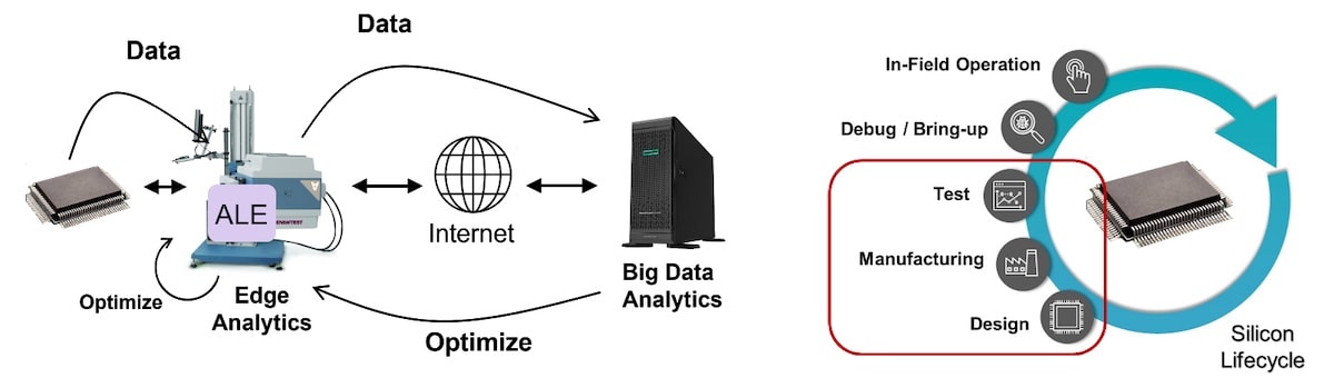
Another strategic acquisition that Synopsys made to start building up its SLM vision was Qualtera back in June 2020, and they provide big data analytics for semiconductor test and manufacturing. The early tools in SLM are well-known to IC design and test engineers, because they include DFT and ATPG. The later tools in SLM are the analytics and in-field optimization.  This is precisely where the latest acquisition of Concertio comes in, because they provide AI-based optimization of a running system. Here’s a graphical flow of the SLM vision, so that you can see all of the areas that it applies to:

Specific IP and EDA tools included within SLM, include:

  • DesignWare PVT monitors
  • Fusion Design Platform – placement of PVT monitors
  • SiliconDash – data analytics for semiconductor manufacturing
  • YieldExplorer – design centric yield management
  • SiliconMax high-speed access IP, TestMAX Adaptive Learning Engine

For in-field operations, the idea is to observer the software running on the system, analyze it, then tune the system. One example that comes to mind is how a vertically integrated company like Apple have optimized how their MacBook Pro laptop  has it’s battery charged to optimize it’s lifespan, because they know how often each app is run, what the power and RAM use for an app is, and can then control clock speeds based on workloads, control the RPM rate of fans and ultimately extend the lifetime of the battery.

Concertio is being used by systems companies to monitor work loads, optimize the compute resources through firmware settings, OS setting and even app settings, or Kubernetes settings on cloud apps. They use reinforcement learning in their AI approach for continuous, realtime optimizations. Users of Concertio technology are reporting improvements in the range of 5-15%.

From a marketing perspective, the SLM tools fall under the platform name SiliconMAX. I learned that the Concertio company was incorporated in New York, while their R&D team is in Israel, and they serve multiple markets, like: Cloud, on-premise compute centers, silicon design, high frequency trading. Synopsys has a good record of treating acquired companies quite well, and you can still visit the concertio.com web site, as they support customers and grow their business.

I could see some similarities in the approaches between the DSO.ai technology and what Concertio offers, as they both use reinforcement learning, so it will be interesting to see what kind of synergy there may be in the future. Stay tuned for more news as Synopsys integrates Concertio technology so that PVT analytics are fed into the system optimization loop, keeping SoCs running reliably.

Related Blogs


A Flexible and Efficient Edge-AI Solution Using InferX X1 and InferX SDK

A Flexible and Efficient Edge-AI Solution Using InferX X1 and InferX SDK
by Kalar Rajendiran on 11-18-2021 at 6:00 am

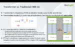
15 Transformer vs Traditional CNN 2

The Linley Group held its Fall Processor Conference 2021 last week. There were several informative talks from various companies updating the audience on the latest research and development work happening in the industry. The presentations were categorized as per their focus, under eight different sessions. The sessions topics were, Applying Programmable Logic to AI Inference, SoC Design, Edge-AI Software, High-Performance Processors, Low-Power Sensing & AI, Server Acceleration, Edge-AI Processing, High-Performance Processor Design.

Edge-AI processing has been garnering a lot of attention over the recent years and accelerators are being designed-in for this important function. Flex Logix, Inc, delivered a couple of presentations at the conference. The talk titled “A  Flexible Yet Powerful Approach to Evolving Edge AI Workloads,” was given by Cheng Wang, their Sr.VP Software Architecture Engineering. This presentation covered details of their InferX X1 hardware, designed to support evolving learning models, higher throughput and lower training requirements. The other talk titled “Real-time Embedded Vision Solutions with the InferX SDK,” was given by  Jeremy Roberson, their Technical Director and AI Inference Software Architect. This presentation covered details of their software development kit (SDK) that makes it easy for customers to design an accelerator solution for Edge-AI applications. The following is an integrated summary of what I gathered from the two presentations.

Market Needs and Product Requirements

As fast as the market for edge processing is growing, the performance, power and cost requirements of these applications are also getting increasingly demanding. And AI adoption is pushing processing requirement more toward data manipulation rather than general purpose computing. Hardware accelerator solutions are being sought after to meet the needs of a growing number of consumer and commercial applications. While an ASIC-based accelerator solution is efficient from a performance and power perspective, it doesn’t offer the flexibility to address the changing needs of an application. A CPU or GPU based accelerator solution is flexible but not efficient in terms of performance, power and cost efficiencies. A solution that is both efficient and flexible will be a good fit for edge-AI processing applications.

The Flex Logix InferX™ X1 Chip

The InferX X1 chip is an accelerator/co-processor for the host processor. It is based on a dynamic Tensor processing approach. The Tensor array and datapath are programmed via a standard AI model paradigm described using TensorFlow. The hardware path is reconfigured and optimized for each layer of AI model processing. As a layer completes processing, the next layer configuration is reconfigured in microseconds. This allows efficiencies approaching what can be expected from a full custom ASIC at the same time providing the flexibility to accommodate new AI models.  This reconfigurable hardware approach makes it well suited for executing new neural network model types.

A Transformer is a new type of neural network architecture that is gaining adoption due to better efficiencies and accuracies for certain edge applications. But transformer’s computational complexity far exceeds what host processors can handle. Transformers also have a very different memory access pattern than CNNs. The flexibility of the InferX technology can handle this.  ASICs and other approaches (MPP for example) may not be able to easily support the memory access requirements of transformers. X1 can also help implement more complex transformers efficiently in exchange for simpler neural network backbone.

The InferX X1 chip includes a huge bank of multiply accumulate units (MACs) that do the neural math very efficiently. The hardware blocks are threaded together using configurable logic which is what delivers the flexibility. The chip has 8MB of internal memory, so performance is not impacted due to being external memory-bound. Very large network models can be run off of external memories.

Current Focus for Flex Logix

Although the InferX X1 can handle text input, audio input and generic data input, Flex Logix is currently focused on embedded vision market segments. Embedded vision applications are proliferating across multiple industries.

The InferX SDK

The SDK is responsible for compiling the model and enabling inference on the X1 Inference Accelerator.

How the Compiler Works

The compiler traverses the neural network layer by layer and optimizes each operator by mapping to the right hardware on X1. It converts TensorFlow graph model to dynamic InferX hardware instances. It automatically selects memory blocks and the 1D-TPU (MACs) and connects these blocks and other functions such as non-linearity and activation functions. And it finally adds and configures the output memory blocks for receiving the inference results.

Minimal effort is required to go from Model to Inference results. The customer supplies just a TFLite/ONNX model as input to the compiler. The compiler converts the model into a bit file for runtime processing of the customer’s data stream on the X1 hardware.

Runtime

API calls to the InferX X1 are made from the runtime environment. The API is architected to be able to handle the entire runtime specification with just a few API calls. The function call names are self-explanatory. This makes it easy and intuitive to implement.

Assuring High Quality

Each convolution operator has to be optimized differently as that depends on the channel depth. Flex Logix engages the hardware, software and apps team to rigorously test the usual as well as the corner cases. This is the diligent process they use to confirm that both the performance and functionality of the operators are met. Flex Logix has also quantized image de-noising and object detection models and verified a less than 0.1% accuracy loss in exchange for huge benefits in memory requirement.

Summary

Customers can implement their accelerator/inference solutions based on the InferX X1 chip. The InferX SDK makes it easy to implement edge acceleration solutions. Customers can optimize the solutions around their specific use cases in the embedded vision market segments.  The compiler ensures maximum performance with minimal user intervention. The InferX Runtime API is streamlined for ease-of-use. The end result is CPU/GPU kind of flexibility with ASIC kind of performance at low-power. Because of the reconfigurability, the solution is future-proofed for handling newer learning models.

Cheng’s and Jeremy’s presentations can be downloaded from here. [Session 2 and Session 10]


Podcast EP49: Where Semifore fits in the design flow

Podcast EP49: Where Semifore fits in the design flow
by Daniel Nenni on 11-17-2021 at 10:00 am

Dan and Mike are joined by Rich Weber, co-founder and CEO of Semifore. Rich describes what the hardware/software interface is, where it fits in the design flow and the importance of a well-documented and robust design. He touches on industry standards, where they help and how Semifore’s products complete the flow. RIch also addresses what comes next with Semifore’s development.

https://semifore.com/

The views, thoughts, and opinions expressed in these podcasts belong solely to the speaker, and not to the speaker’s employer, organization, committee or any other group or individual.


Register Management is the Foundation of Every Chip

Register Management is the Foundation of Every Chip
by Mike Gianfagna on 11-17-2021 at 6:00 am

Register Management is the Foundation of Every Chip

Virtually every chip today runs software. And that software needs to interact with and control the hardware on the chip. There are typically many interfaces to manage as well as dedicated hardware accelerators to coordinate. In fact, many of those hardware accelerators are present only to support the execution of the software in a specific way. Most AI algorithms work like this. If you’re a software engineer, you will recognize the need for device drivers to accomplish these tasks. If you’re an architect, you know the register map is what makes the device drivers work. Managing those registers is a complex task and Semifore has a great white paper that explains the moving parts of this process. Read on to see why register management is the foundation of every chip.

The HSI

The register map implements something often called the hardware/software interface, or HSI. It’s the critical part of the design that ensures the device drivers can do what they’re supposed to. Getting the details of this part of the design correct, at the beginning is an important part of a successful project. It doesn’t end there, however.  A complex HSI can have millions of 64-bit registers. During design, bits in those registers can change quite often, many times per day. That necessitates creating a new version of the HSI and all the supporting documentation that often as well.  A methodology with substantial automation is the only way forward in this situation.

Where Semifore Fits

Semifore focuses exclusively on addressing the development of a verified, correct-by-construction HSI and propagating all the required formats to the various members of the design team. Ensuring everyone on the team is using consistent, up-to-date information is a critical item for smooth execution. Team members that need a unique format describing the HSI include RTL designers, verification engineers, software engineers and documentation staff. You can learn more about Semifore in this interview with Rich Weber, Semifore’s co-founder and CEO.

The White Paper

The Semifore white paper provides a great overview of the challenges of building the HSI and details that methodology with substantial automation I previously mentioned. The benefits of such a methodology are outlined in the white paper, as well as the pitfalls of trying to do it yourself.

A product design cycle is detailed to help you understand how the methodology fits. Aspects covered include:

  • Product definition phase
  • Product implementation phase
  • RTL verification
  • Software development
  • Documentation

Each section includes a detailed look at best practices and the benefits of following those practices. This document summarizes many years of experience Semifore has logged helping customers design highly complex chips. Reading it will save you a lot of time. You can access the white paper here.

One of the very challenging aspects of the HSI is managing all the objects and parameters that define its structure and behavior. There are industry standards that address part of this problem. There are also aspects not covered by those standards. It turns out Semifore has a solution for this problem as well. They have developed a language that is part of its product offering that picks up where the standards leave off.

It’s a way to build a real executable specification of your design. As a bonus, here is a link to the document that explains all the formats that need to be tracked, and how to capture them. After reading these white papers, you will appreciate why register management is the foundation of every chip, and how to build a solid foundation.

Also Read:

Webinar: Semifore Offers Three Perspectives on System Design Challenges

CEO Interview: Rich Weber of Semifore, Inc.


Where is the Monument of the Silicon Glen?

Where is the Monument of the Silicon Glen?
by Asen Asenov on 11-16-2021 at 10:00 am

NEC Plant Livingston

In 1991, I arrived in Glasgow to become a lecturer in Glasgow University, attracted by the Silicon Glen – the heart of semiconductor manufacturing in Europe. Here are few facts:

  • The larges semiconductor plant in Europe at that time was the NEC DRAM manufacturing site in Livingstone. When I visited the plant, I was mesmerized by the robot cars carrying the wafer batches between the processing stations. The plant closed in 2001 at the time of the great semiconductor industry downturn.
  • The first Motorola MOS plant was built in East Kilbride. I used to take students from my semiconductor course to visit. Usually in the parking you would see 6-7 Porsches. The Motorola guys were testing their Porsche chip sets on the cars and all Motorola managers were driving Porsches. The plant closed in 2003 also due to the semiconductor downturn.
  • The National Semiconductor plant in Greenock was pioneering the bipolar and BiCMOS technology. It is the longest standing semiconductor manufacturing plant in Scotland – from 1971 until now. After a sale to Texas Instruments the plant now has new owners – Diodes securing 300 jobs.
  • Perhaps the most sustainable small scale semiconductor operation in Scotland is Semefab. Founded in 1986 it is still going, offering foundry services for MEMS, CMOS, Opto-CMOS, Linear IC, BiCMOS, ASIC and Discrete Semiconductor device technologies.

Although not exactly semiconductor manufacturing, I would like to mention the IBM electronic manufacturing site in Spango Valley Greenock which had over 5000 staff at its peak. Combined with National this was almost 8000 staff in Greenock.

The Alba Centre in Livingstone established in 2000 around the idea of CMOS IP development in Scotland with Cadence in its heart was the Swan Song of the Silicon Glen. As a Head of the Department of Electronics and Electrical Engineering at Glasgow University at that time I was involved in the delivery of an MSc course in chip design for the 2000 future employees of Cadence who never came.

The hard lesson is that due to the semiconductor market turbulence inward investments from the big multinationals cannot sustain semiconductor expertise and manufacturing in our country. If a certain level of the vital advanced semiconductor manufacturing is to be resurrected in the UK perhaps the government need to think about a new model. However, these days creating advanced semiconductor manufacturing from scratch is only possible in countries with waste resources like China. For the UK will be very important to join forces with Europe and US in this area to remain competitive.


Siemens EDA Automotive Insights, for Analysts

Siemens EDA Automotive Insights, for Analysts
by Bernard Murphy on 11-16-2021 at 6:00 am

Siemens auto electronics min

There is a classical approach to EDA marketing, and semiconductor marketing at times, which aims exclusively at technical customers and the businesspeople immediately around those experts. The style is understandable and necessary. Those folks are the direct influencers and buyers of the products we are promoting, so we must capture and hold their attention. But many times this focus also seems to be assumed sufficient. We only need to speak to domain experts because the subject matter is far too complex for anyone else to understand. Besides, many attempts have been made to popularize the value of what we do to the larger world – analysts, investors, governments, and consumers – with questionable success. Beyond facile media comparisons, the gulf between what we do and how it affects large markets appears too wide to bridge.

Why is it important to speak to a larger audience?

Business success isn’t determined solely by customers and by being better that the competition. For an extreme example, look at Intel, now leveraging US government enthusiasm for rebuilding domestic semiconductor fab capacity. There are more immediate examples for the rest of us semiconductor types.

When a customer plans a large commitment to a vendor, they don’t only work through a technical checklist. They want to understand business characteristics of the vendor – financial performance and stability to support a long-term commitment. They want to understand what analysts, the press and other customers think of vendor market directions and ability to innovate; are these aligned with the customer?

The same applies to a potential buyer – of your company. Or a company you want to buy. The bond markets too, if you want to raise money. And of course, it applies to your stock price. Investors want to find undervalued companies with lot of growth potential, not stuck-in-a-rut companies.

Wider audiences need a different message

These audiences have limited if any appetite for technical specs. They want to understand why what you do is important and your track record in delivering on commitments to big name customers. Convincing them that you are a hot company to watch, the kind of company they should enthusiastically recommend, requires a different kind of marketing. Messaging of this kind should talk primarily about your customers’ customers (auto OEMs) goals and what it takes to meet those goals. Only towards the end does the story get into what part (at a high level) you can play in helping them meet those goals.

This is the Hero’s Journey, of which I’m a huge fan. The larger marketing world beyond semiconductors is already on-board. If you want more detail from a semiconductor perspective, read the book. I’m very encouraged to see Siemens EDA producing white papers in this class. This shows to me that they are fully embracing the larger perspective of Siemens marketing. Recognizing that they need to speak to and influence a much more diverse group than their traditional engineer, architect and product manager audience. Good for them!

Verification and validation for advanced cars

Now I’ve spent most of this blog waxing lyrical on why Siemens is doing this (see?), I should spend a little on what the paper is about 😎.  The first ~50% of the paper is on what automakers are aiming to deliver in SAE level 3 and beyond. And the opportunities and challenges in delivering to those expectations. Great start. We don’t all have a common understanding here, especially since the ground keeps shifting on when this might happen. Setting the context is important – the Call to Adventure.

The next ~25% of the paper is on development and verification implications. In being able to model, verify and validate hardware in the loop with other components of the system. This is critically important for autonomy modeling and testing. Where digital twin analysis over millions, even billions of virtual miles is becoming unavoidable. This is the Ordeal auto OEMs already face.

The last ~25% of the paper introduces how Siemens can help through their PAVE360 platform. In Hero’s Journey terms, where you as their Mentor explain to your customer how your solution can help them achieve their goals.

Nice job! You can read the white paper HERE.

Also Read:

Tessent Streaming Scan Network Brings Hierarchical Scan Test into the Modern Age

Minimizing MCU Supply Chain Grief

Back to Basics in RTL Design Quality


Tessent Streaming Scan Network Brings Hierarchical Scan Test into the Modern Age

Tessent Streaming Scan Network Brings Hierarchical Scan Test into the Modern Age
by Tom Simon on 11-15-2021 at 10:00 am

Streaming Scan Network

Remember when you had to use dial up internet or parallel printer cables connected directly to the printer to print something? Well even if you don’t remember these things, you know that now there is a better way. Regrettably, the prevalent methods used for hierarchical Design for Test (DFT) still look at lot like this – SoC level DFT has not kept up with design scaling. Fortunately, Siemens EDA has developed an entirely new methodology for connecting core level scan to the top level. Let’s acknowledge that hierarchical scan was a huge step forward. But, accessing the cores has always been done with methods that look like a room full of telephone operators individually connecting calls.

Siemens has published an article titled “Tessent Streaming Scan Network: A no-compromise approach to DFT” that clearly lays out the problems endemic with implementing full chip test using core level scan and pin-mux connections. The paper describes the Streaming Scan Network (SSN) approach that they have developed to address these problems. Using the old pin-mux technique, chip designers have to plan up front how to efficiently use a limited number of chip-level pins to facilitate testing. Critical decisions have to be made early in the design phase and are difficult to change later in development. Even running identical blocks in parallel runs into limitations. Up front decisions have to be made about which sets of identical blocks can be run in parallel. Pipelining to each block must match, and the results need to come back serially, etc. Even here there is no free lunch. For most other types of blocks it is equally messy.

To highlight the limitations of the pin-mux approach, the Siemens paper discusses several other problems. Hardwired buses need to be the proper width and have to be routed in advance in anticipation of how patterns will be run later. Branches that have blocks with shorter scan chains will leave bandwidth wasted. The routing itself can be problematic, especially when block to block connections in the chip are only are made with abutment.

Streaming Scan Network used in a 6 core design

Tessent SSN solves the problems with the pin-mux scan approach, while at the same time adding flexibility and making test operations measurably more efficient. Each core is fitted with a Streaming Scan Host (SSH) which acts as a local intelligent controller. Each SSH has two external connections – an IJTAG 1687 interface for coordinating test activities and the parallel SSN data bus. The SSN bus, while parallel, is independent of the number or size of the scanned cores. Scan data is sent in packets. The scan data for each target block is completely abstracted from the SSN packets, which can be intermixed and carry scan data of any width. The result is that the SSN can operate at full capacity and unwrap the scan data where it is used to interface with the core’s internal scan chain.

Parallel testing of identical blocks is made easy with scan packet delivery in parallel, regardless of the location on the SSN. Tests can be run in parallel, and local results checking can flip a pass/fail bit for each instance. The bus can also help adjust for slower internal shift frequencies by sending faster packets that are narrower to keep in sync with these blocks. Having a packetized smart network for moving scan and test data anywhere on the chip means that test strategies can adapt to the specifics of the design, even after tapeout.

The article offers a lot more detail on the specifics and advantages of Siemens Streaming Scan Network. It certainly moves DFT from the age of modems and parallel printer cables into the modern age of broadband and networked printers. The full article is available on the Siemens website along with full product information on Streaming Scan Network.

Also Read:

Minimizing MCU Supply Chain Grief

Back to Basics in RTL Design Quality

APR Tool Gets a Speed Boost and Uses Less RAM