In the modern world, the semiconductor industry stands at the heart of technological innovation. From smartphones and laptops to advanced medical devices and artificial intelligence systems, nearly every piece of contemporary electronics depends on increasingly sophisticated microchips. Among the leading companies driving this progress is Taiwan Semiconductor Manufacturing Co., Ltd. (TSMC), the world’s largest pure-play semiconductor foundry. Through continuous research, advanced manufacturing techniques, and aggressive scaling strategies, TSMC has played a pivotal role in pushing the boundaries of what is possible in chip fabrication.
As semiconductor technology advances, one of the most critical goals is scaling down device dimensions. Smaller transistors allow for higher device density, faster switching speeds, and lower power consumption. However, shrinking dimensions introduces immense engineering challenges. At technology nodes such as 5nm and beyond, even minute variations in patterning can significantly impact device performance and yield. Achieving precise control over distances between features, such as the “end-to-end” spacing between adjacent structures, becomes increasingly difficult as these distances approach tens of nanometers.
Traditional lithographic processes often require multiple patterning and etching steps to achieve extremely tight spacing. In earlier approaches, forming patterns with very small end-to-end distances might involve three separate lithography steps combined with multiple etching stages. Each additional step increases production time, cost, and the potential for alignment errors. Overlay inaccuracies between masks can lead to critical dimension variations, negatively affecting device reliability and manufacturing yield. Therefore, reducing the number of processing steps while maintaining or improving precision is a key objective in advanced semiconductor fabrication.
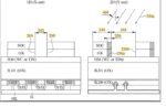
One important innovation involves using a single lithographic process combined with carefully engineered etching techniques to achieve sub-35 nm end-to-end distances. Instead of relying on multiple pattern transfers, this approach begins with forming unidirectional features in a photoresist layer using advanced lithography, such as EUV lithography. EUV uses very short wavelengths of light to define smaller features than previously possible with deep ultraviolet systems. By carefully designing the initial pattern and then applying a controlled angled etch process, the effective length of features can be modified without changing their width.
The angled etch technique is particularly significant. By directing ion beams at specific angles relative to the substrate surface, engineers can selectively trim or extend certain dimensions of patterned structures. For example, the length of a feature along one direction can be increased, thereby reducing the end-to-end spacing between neighboring features. This allows a final pattern to achieve tighter spacing than originally defined in the photolithography mask. Importantly, this method maintains the critical width dimension while adjusting only the desired axis, enabling precise dimensional control.
Such process optimization provides several advantages. First, it reduces the number of required lithography steps from three to one, cutting down cycle time and manufacturing costs. Lithography is one of the most expensive and time-consuming steps in semiconductor fabrication, so eliminating even a single lithography stage can yield substantial economic benefits. Second, fewer process steps reduce the risk of cumulative defects and misalignment errors, improving overall yield and device reliability. Third, streamlined processing enhances throughput in high-volume manufacturing environments, enabling faster delivery of advanced chips to market.
In devices such as FinFETs, which are widely used at advanced nodes, precise pattern control is especially crucial. FinFET architectures rely on three-dimensional channel structures that improve electrostatic control compared to planar transistors. However, their 3D geometry increases fabrication complexity. Maintaining consistent spacing between contacts, gates, and interconnects ensures proper electrical isolation and performance. Techniques that achieve tighter end-to-end distances without increasing process complexity directly support the continued scaling of FinFET and future transistor architectures.
Ultimately, innovation in semiconductor manufacturing is not just about making features smaller; it is about doing so efficiently, reliably, and economically. Companies like TSMC continue to invest heavily in process integration, materials engineering, and advanced patterning technologies to sustain progress beyond the 5nm node. By combining advanced lithography with creative etching strategies, the industry can overcome scaling barriers that once seemed insurmountable.
Bottom Line: As global demand for computing power grows driven by artificial intelligence, 5G communications, autonomous vehicles, and high-performance computing, the importance of such innovations will only increase. The ability to control nanometer-scale distances with extreme precision represents not just a technical achievement, but a foundational capability that shapes the future of modern technology.
Also Read:
TSMC and Cadence Strengthen Partnership to Enable Next-Generation AI and HPC Silicon
TSMC vs Intel Foundry vs Samsung Foundry 2026
TSMC & GCU Semiconductor Training Program: Preparing Tomorrow’s Workforce