A recent analysis highlighted by MIT Technology Review puts the energy cost of generative AI into stark perspective. Generating a simple text response from Llama 3.1-405B—a model with 405 billion parameters, the adjustable “knobs” that enable prediction—requires on average 3,353 joules, nearly 1 watt-hour (Wh). Once cooling and supporting infrastructure are factored in, that figure effectively doubles to about 6,706 joules (~2 Wh) per response.
The picture becomes even more striking with video. The same study found that producing just five seconds of low-resolution video at 16 frames per second with the open-source CogVideoX model consumed approximately 3.4 million joules, nearly 1 kilowatt-hour (kWh), as measured via CodeCarbon. To put that into perspective, this is roughly the amount of electricity a typical household appliance uses in an hour.
To scale this scenario, public estimates suggest that in mid-2025, platforms such as ChatGPT were handling over 2.5 billion queries per day. Even conservatively extrapolated, generative AI systems were dissipating energy on the order of gigawatt-hours daily, a level of consumption that rival industrial operations.
This raises two urgent questions:
- Why does AI inference consume so much energy?
- More importantly, can processor architecture be redesigned to dramatically reduce this cost?
The answer lies not only in model size, but in the silicon beneath it. AI processor architecture is no longer just a performance concern, rather it is a defining factor in the energy efficiency, scalability, and sustainability of artificial intelligence itself.
GPGPU: The Right Architecture for the Wrong Workload
GPGPUs are built around a micro-level execution model implemented on the Single Instruction, Multiple Threads (SIMT) model. In this model, performance is achieved by launching thousands of tiny threads, each operating on small pieces of data. Developers are expected to carefully coordinate these threads so that, together, they complete a larger computation.
This approach emerged from computer graphics, where workloads are highly irregular and branching behavior is common. SIMT excels in that environment because it allows thousands of threads to hide latency and tolerate divergence. However, when applied to artificial intelligence workloads the mismatch becomes apparent. AI computations are highly structured, repetitive, and mathematically regular, yet SIMT forces them to be expressed through an abstraction designed for far more chaotic workloads.
As a result, a significant fraction of execution time in SIMT-based systems is not spent performing useful mathematical work. Instead, it is consumed by what can be thought of as a management overhead. The hardware and software stack must constantly schedule threads, synchronize execution, handle divergence within warps, and coordinate memory accesses across deep hierarchies. As models grow larger and latency constraints tighten—particularly in real-time or interactive inference scenarios—this overhead begins to dominate overall performance.
VSORA: Redefining the Rules of the Game in AI Processors
This is the context in which VSORA enters the picture. With more than a decade of experience designing advanced digital signal processing architectures, VSORA approaches AI computation from a different starting point. Its background lies in deeply pipelined processors with rich instruction sets capable of executing complex operations in a single clock cycle. Rather than adapting an existing GPU model, VSORA leveraged this expertise to design a processor architecture specifically tailored for large language model inference, both in the cloud and at the edge. The goal was not incremental improvement, but a clean break from the inefficiencies inherent in GPGPU-based designs.
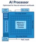
VSORA MPU: A Structural Shift in How AI Gets Computed
At the heart of this new approach sits the VSORA Matrix Processing Unit, or MPU. To appreciate how it differs, consider what happens when the basic unit of computation changes. In SIMT systems, threads are the atomic unit, and everything—from memory layout to scheduling—is organized around them. VSORA discards this assumption entirely. Instead of threads, the MPU treats tensors—multidimensional arrays representing matrices and vectors—as the fundamental unit of work.
In practical terms, this means that instructions operate on entire tensors at once. The programmer describes a mathematical operation, such as a matrix multiplication or transformation, without specifying how the work should be divided among thousands of execution contexts. The hardware itself is responsible for decomposing the operation, distributing it across compute resources, and executing it efficiently. This shift moves complexity out of software and into silicon, where it can be handled deterministically and at far lower cost.
For developers, this tensor-centric abstraction simplifies both programming and reasoning about performance. There is no need to manually manage threads, worry about warp divergence, or tune kernel launch parameters. Because execution management is internalized by the hardware, performance becomes more predictable, and developers can focus on correctness and algorithmic structure rather than orchestration.
Massive Register File and Tightly Coupled Memory
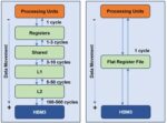
One of the most visible consequences of this architectural philosophy appears in the MPU’s memory design. Traditional processors rely heavily on multi-level cache hierarchies that attempt to predict which data will be needed next. While caches work well in many general-purpose scenarios, they are fundamentally probabilistic. When predictions fail, cache misses introduce long and unpredictable delays, which are especially problematic for real-time inference.
VSORA replaces this uncertainty with a large, explicitly managed memory structure. The MPU includes a massive, software-visible register file implemented as several megabytes of tightly coupled memory, or TCM. This memory sits physically close to the compute engines and behaves like a flat, deterministic scratchpad rather than a cache. Its capacity is sufficient to hold entire weight matrices and intermediate activations on-chip, allowing the system to operate without relying on speculative caching behavior. See figure 1.
By designing around tensor-level locality and provisioning enough on-chip storage to support it, the MPU ensures consistent access latency. As long as the working set fits within the TCM, memory access times remain uniform and predictable. This eliminates the performance cliffs that often occur when cache hierarchies are overwhelmed, a common issue in large neural networks.
Continuous Pipelining and Deterministic Throughput
Once data is resident in the TCM, the MPU leverages highly efficient prefetching techniques to minimize latency. Instead of treating AI workloads as a series of discrete kernel launches, VSORA views them as sustained computational flows. An intuitive way to think about this is as an assembly line: once the pipeline is filled, new results emerge at a steady rate every cycle.
This pipelining operates at multiple levels. At the micro-architectural level, data streams continuously into compute units without stalls. At the instruction level, preparation and execution overlap so that hardware resources remain fully utilized. The architecture also allows multiple MPUs to be chained together, enabling data to flow directly from one unit to the next without detouring through external memory. After an initial warm-up period, throughput stabilizes and becomes largely independent of the complexity of individual operations.
Automated Data Layout and Reduced Software Burden
Another area where the MPU reduces developer burden is data layout. On many accelerators, achieving high performance requires manually rearranging data in memory to match hardware-specific access patterns. This process is error-prone, time-consuming, and often ties software to a specific architecture.
VSORA intentionally removes this responsibility from the programmer by introducing a memory access abstraction. The MPU hardware automatically handles alignment, padding, swizzling, and internal data reordering needed to sustain peak bandwidth. Developers work with tensors as abstract mathematical objects, while the hardware transparently performs the low-level transformations required for efficient execution. This approach not only improves productivity but also reduces performance fragility caused by subtle layout mismatches.
These architectural choices make the VSORA MPU particularly well suited for inference workloads, where latency and predictability matter more than raw peak throughput. Unlike GPUs, which often require large batch sizes to amortize overheads and reach high utilization, the MPU remains efficient even with batch size one. This is critical for real-time applications such as robotics, autonomous systems, and interactive AI, where waiting to accumulate large batches is not an option.
Dataflow Execution Model
In conventional multi-core and multi-accelerator systems, scaling often introduces diminishing returns due to synchronization overhead and shared memory contention. Additional compute resources increase coordination costs, reducing effective throughput.
Instead of treating each processing unit as an independent island, multiple MPUs are connected into a single, deeply pipelined dataflow graph. The output of one MPU becomes the direct input of the next, enabling true zero-copy execution at the hardware level.
Each MPU maintains its own TCM, allowing large models to be partitioned cleanly across units. Data moves directly between register files rather than through external memory interfaces, which is especially advantageous for the hot data paths common in modern neural networks. As models scale, throughput remains flat and predictable as long as active tensors fit within the available TCM.
Simplified Scaling and System-Level Efficiency
From a system-level perspective, this results in an architecture that scales without imposing additional complexity on developers. Instead of implementing intricate tiling strategies, synchronization mechanisms, and scheduling logic, programmers define tensor flows and dependencies. The hardware autonomously manages execution, handshaking, and scheduling, ensuring consistent performance even under tight latency constraints.
This makes the VSORA architecture especially conducive to high-pressure environments such as cloud inference platforms, edge deployments, and autonomous systems, where strict latency budgets leave no room for scheduling inefficiencies or unpredictable stalls.
Conclusion
By eliminating kernel launch overhead and dismantling the traditional memory wall between layers, the VSORA Matrix Processing Unit redefines AI efficiency at its core. It delivers near-peak hardware utilization even at batch size one—something conventional accelerators simply cannot achieve. Performance is no longer dependent on artificial batching to mask architectural inefficiencies.
This makes the architecture uniquely suited for interactive and real-time AI, where milliseconds determine safety, usability, and user experience. From real-time autonomy to fluid conversational systems, VSORA prioritizes determinism, latency consistency, efficiency, architectural simplicity, and cost effectiveness over brute-force parallelism.
Equally transformative is the ease of adoption. There is no new programming model, no proprietary language, no disruptive toolchain shift. Developers continue using familiar frameworks such as TensorFlow, PyTorch, or ONNX—without rewriting models or retraining teams. Transitioning to VSORA requires no paradigm change, only performance gains.
In short, the VSORA MPU does not just accelerate AI workloads—it removes the structural bottlenecks that have defined them.
Also Read:
VSORA Board Chair Sandra Rivera on Solutions for AI Inference and LLM Processing
Silicon Valley, à la Française
Inference Acceleration from the Ground Up