David has almost 25 years of leadership experience in the semiconductor industry. Prior to joining Pragmatic, he served as Chief Strategy Officer at Micron Technology, Inc. He also spent six years at Intel Corporation in various roles, including General Manager of the Programmable Solutions Group, where he led the multi-billion-dollar FPGA and Structured ASIC business on a global basis.
Tell us about your company?
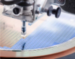
Pragmatic is a UK-based leader in flexible integrated circuit technology and semiconductor manufacturing. We use thin-film semiconductors to create ultra-thin, flexible integrated circuits, known as FlexICs, that are significantly cheaper and faster to produce than silicon chips – we’re talking days, rather than months, and potentially sub-penny price points for certain applications.
As you can imagine, this makes FlexICs a compelling alternative to silicon for lots of mainstream electronics applications, as well as enabling new applications that may not have been possible previously, either because of cost or due to silicon’s rigid form factor.
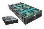
We also offer a Fab-as-a-Service model that enables secure, dependable, localized semiconductor supply. The reduced complexity of our innovative manufacturing and process technology allows for compact fabs that are orders of magnitude lower in terms of cost, and physical and environmental footprint, compared to silicon.
We are headquartered in Cambridge, UK with production lines in Durham in the northeast of England.
What problems are you solving?
Many of the most impactful Internet of Things applications that seek to harness AI at scale will depend on item-level intelligence and ubiquitous connectivity. We’re talking billions – and, ultimately, trillions – of smart physical objects. For a number of reasons, silicon chips alone can’t achieve that, and we aim to plug the gap.
Recently, we’ve become all too familiar with the impact of brittle supply chains. Even if we assume that similar shocks won’t reoccur – while being cognizant that they likely will – there’s simply not enough fab capacity in the world pumping out the right kind of silicon chips to address the incoming tsunami of demand. And it wouldn’t be cost-effective to use silicon for many of these workloads even if there were. The long lead times and high costs associated with silicon chip design mean that it is best reserved for creating complex, higher-spec chips in applications that require that level of performance.
We operate at the other end of the scale. Our agile technology platform, which leverages industry standard EDA tools, and rapid production cycles allows you to target a specific application and customize to meet the performance required. This means you can accelerate time to market – and even make changes as your requirements shift, without incurring crazy re-spin costs or long turnaround times.
To be clear, we’re not trying to compete with leading-edge silicon, here. Today’s FlexICs deliver just enough performance for a very wide range of simple tasks. But that simplicity is their strength and, it’s what allows them to provide ubiquitous intelligence and connectivity, at a price point and low environmental impact that’s simply not achievable with silicon.
What application areas are your strongest?
One of our largest, near-term opportunities is in Radio Frequency Identification (RFID) and Near-Field Communication (NFC) applications that use smart and reusable packaging to dramatically enhance supply chain optimization and consumer engagement.
There’s huge consumer demand, and increasing regulatory requirements, for brands to improve supply chain traceability and reduce waste. However, that can be challenging for high-volume, lower-value goods and packaging – often, the numbers just don’t add up. But when you’re talking about item-level intelligence at a price point of pennies or less, it’s a game changer.
Companies have been quick to spot this potential: for example, we’re working on a trial with a major UK supermarket chain that’s investigating the deployment of smart reusable packaging at scale. It’s one of many exciting opportunities to change the way we think about plastic and waste in everyday consumables.
We’re also looking at a range of healthcare applications, from temperature sensors in health monitors to smart bandages – an area where the thinness and flexibility of our chips can really make a difference to wearer comfort.
We also see significant opportunities in consumer wearables and even toys and games. In an age where it can be hard to get kids off screens, boosting the interactivity levels of their ‘analogue’ toys by seamlessly adding intelligence holds a lot of appeal.
What keeps your customers up at night?
In recent years, semiconductor supply has been a key issue – concerns over global supply chain resiliency have been reflected by the US and EU Chips Acts and the UK’s recent semiconductor strategy announcement.
There’s now a push to onshore semiconductor fabrication, but if you’re looking to add silicon capacity on an advanced or even a mainstream node, it’s not something you can do quickly – or, often – economically a single fab typically costs billions of dollars to build and takes many years to be deployed. But deployment of new flexible semiconductor fabs takes far less time and because they’re modularly scalable: you can achieve cost-effective, localized manufacturing with a cost structure that’s significantly lower than legacy silicon fabs. And you can do it quickly, too!
Beyond that, as demand for semiconductors continues to grow, there’s increasing pressure for the industry to tackle its carbon footprint. Because our unique production process omits many of the resource-intensive, high-temperature stages of silicon semiconductor manufacturing, it uses orders of magnitude less water and energy, and significantly fewer harmful chemicals and gases. In particular, we don’t create or release PFAS – forever chemicals. While it’s not always easy to lay your hands on the relevant industry figures to make an exact comparison, initial calculations show that chips from our fabs could have a carbon footprint well over 100 times lower than those manufactured in typical silicon fabs.
What does the competitive landscape look like and how do you differentiate?
Currently, no other company has a comparable offering in commercial production and, to our knowledge, competing approaches in research and development are still many years away from volume manufacturing at scale.
For existing applications using silicon chips, we compete against ‘legacy node’ foundries, but in practice, our differentiation on cost, form factor, production cycle times, sustainability and security of supply gives us unique advantages wherever our performance meets the application requirements.
What new features/technology are you working on?
Innovation is the essential fuel of our growth plans. We’re currently ramping up our second fab in the northeast of England, which will be the first 300mm wafer fab in the UK. It has the capacity to deliver billions of ICs per year, and we’ll be commissioning additional lines at the site to bring capacity to tens of billions of ICs in 2025.
Our next-generation process technology will deliver a 10X reduction in power consumption and significant area reductions, generation-on-generation, for our RFID product lines and to our foundry customers.
We’ll also be advancing our RFID technology roadmap to support expanded NFC features and Ultra High Frequency (UHF) RFID applications, enabling breakthrough solutions at scale in what is one of the fasted growing segments in the semiconductor industry.
In parallel, we’re investing to deliver new, cost-optimized, ultra-thin sensing and control capabilities that further expand our addressable foundry market for a host of exciting, high-impact applications in the consumer, healthcare and industrial segments.
How do customers normally engage with your company?
Our core offering is the provision of foundry services to our customers. They design the chip, or partner with us to design it, then we manufacture and deliver the diced FlexIC wafers – just like companies such as TSMC or Global Foundries in the silicon space.
We also produce RFID products as ICs that are integrated into intelligent labels and smart packaging solutions by leading brands or RFID tag and solution providers.
Finally, Fab-as-a-Service is our unique solution for the future of distributed semiconductor manufacturing. By installing and operating a fab at the customer’s site of choice, we provide secure, dedicated, localized capacity and the most attainable route to cost-effective, scalable fabrication.
We’re excited for the future. By matching our unique technology with a disruptive business model – and our customers’ innovation – we’re confident that we can change the face of semiconductors, facilitating ubiquitous connectivity and solutions to some of the world’s most pressing data challenges.
Pragmatic Semiconductor
Also Read:
CEO Interview: Dr. Meghali Chopra of Sandbox Semiconductor
CEO Interview: Dr. J Provine of Aligned Carbon
CEO Interview: Vincent Bligny of Aniah