When Morris Chang left Texas Instruments in 1983 to found TSMC, he was not merely starting a new company—he was proposing a new industrial logic. Chang recognized that semiconductor manufacturing had become so capital-intensive that it could no longer survive as just one function inside a vertically integrated company. His answer was radical for its time: specialize. Let foundries manufacture, let fabless companies design, and let scale economics determine who survives. Over the next four decades, that model reshaped the entire semiconductor industry.
But the conditions that made the pure-play foundry model dominant are changing again.
As process scaling slows, product lifetimes lengthen, and differentiation shifts away from raw transistor density, manufacturing alone is no longer sufficient to define competitive advantage—especially outside the consumer and cloud-compute markets. Increasingly, value is migrating up the stack, toward system enablement: hardened IP, software continuity, platform longevity, and predictable lifecycle support. In this environment, foundries are no longer just wafer suppliers. They are becoming infrastructure providers.
Seen in that light, GlobalFoundries’ recent acquisition of Synopsys’ CPU IP business—including the ARC processor family—marks something more significant than a portfolio expansion. It signals a second evolution of the foundry model itself. Where Morris Chang separated manufacturing from design to survive the economics of scaling, today’s foundries are selectively reintegrating high-value hard IP to survive the economics of maturity.
This is not a retreat to the IDM era. It is a recognition that in long-lifecycle markets—automotive, industrial, infrastructure, and embedded systems—customers increasingly demand platform certainty, not just wafers. The foundry model is not being abandoned. It is being adapted.
As traditional scaling economics weaken and capital intensity rises, competitive advantage—especially outside consumer and hyperscale compute—shifts from raw transistor density to lifecycle execution and design enablement. “In embedded and industrial markets, leading suppliers explicitly commit to 10–15+ year availability and continuity-of-supply, reflecting customer demand for long-lived platforms rather than frequent redesigns.”
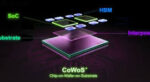
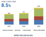
At the same time, the semiconductor IP business has become a multi-billion-dollar market opportunity (roughly $7–8B annually, according to MarketsandMarkets), with the Asia Pacific region, predominately China, holding the largest share. Moreover, it is still growing, with recent industry tracking showing strong IP revenue acceleration. Foundries are responding by expanding from wafer output into “design infrastructure”—ecosystems of qualified IP, certified EDA flows, PDKs, DFM, packaging, and services—exemplified by programs like TSMC’s OIP. In that environment, foundries are no longer just wafer suppliers; they are becoming platform and infrastructure providers for whole product lifecycles.
A Foundry Built by Accumulation
GlobalFoundries did not arise from a single founding moment. It was assembled over time through a sequence of structural decisions, each responding to a different pressure in the semiconductor industry.
The process began in 2008–2009, when AMD spun off its manufacturing arm to escape the escalating capital demands of the IDM model. The move preserved AMD’s access to advanced production while freeing its design organization from an unsustainable cost structure.
That spinout would not have been possible without Mubadala Investment Company, which supplied the long-horizon capital and ownership stability AMD lacked. Mubadala ultimately took an 82% stake in the new foundry, insulating it from short-term financial pressures and enabling a strategy focused on durability rather than speed.
Mubadala then expanded GlobalFoundries’ footprint by acquiring Chartered Semiconductor in Singapore. This move transformed GF from an AMD carve-out into a geographically distributed foundry with real scale, adding multiple fabs, a diverse customer base, and specialty-process breadth.
The final foundational piece arrived in 2014, when IBM exited semiconductor manufacturing and transferred its East Fishkill and Essex Junction fabs—along with its advanced R&D organization and long-term POWER and Z supply agreements—to GlobalFoundries, even paying the company to assume the operations. This infusion of U.S. engineering talent and SOI-driven process technology elevated GF from a mid-range player to a foundry with world-class capabilities in specialized logic.
Taken together, these moves produced a company built by accumulation rather than invention: AMD contributed manufacturing DNA, Abu Dhabi provided capital and industrial patience, Chartered added global scale, and IBM delivered advanced technology. The result is a foundry whose strategy diverges sharply from firms built solely to chase leading-edge nodes. Ironically, AMD relies on TSMC for its leading edge FinFet process.
Two Electronics Universes
At the highest level, the global electronics industry has organized itself around two distinct competitive universes.
The first is consumer and cloud compute: smartphones, PCs, data centers, and hyperscale AI. This universe is driven by peak performance per watt, rapid product cycles, and relentless transistor density scaling. Capital intensity is extreme, product lifetimes are short, and a small number of customers account for a disproportionate share of demand. Manufacturing here has converged on a narrow set of players—TSMC foremost, with Samsung and Intel as the only credible peers at the leading edge.
The second universe, where GlobalFoundries squarely operates, is physical, embedded, and infrastructure electronics. This includes automotive systems, industrial automation, RF connectivity, power electronics, aerospace and defense, medical devices, energy systems, and embedded control and inference. Success in this universe is defined not by headline performance but by reliability, deterministic behavior, qualification, and supply continuity. Product lifetimes stretch over decades, not years.
Comparing GF to TSMC Misses the Point
TSMC, Samsung, and Intel compete in a three-player arena where scale, redundancy, and geopolitical resilience are existential requirements. Each new node demands tens of billions of dollars in capital investment, and the penalty for execution failure is severe.
GlobalFoundries deliberately exited this race. In doing so, it avoided the “middle squeeze” that eliminated many other foundries—companies that were neither large enough to win at the leading edge nor differentiated enough to command durable customers.
Instead, GF rebuilt around markets that value stability over novelty. Automotive, industrial, RF, power, and infrastructure customers do not want to requalify silicon every two years. They want predictability, long-term availability, and conservative process evolution. For these customers, a mature node that improves steadily over time is often more valuable than a bleeding-edge node with a short commercial half-life.
This is why GF appears to “sit by itself” while TSMC has Intel and Samsung as peers. That asymmetry reflects different market physics—not competitive weakness.
Process Innovation Without Density Obsession
Exiting the leading-edge race did not mean exiting process innovation. GlobalFoundries exited the transistor-density race, not the process-generation race that matters to its customers.
GF continues to advance performance, power efficiency, and reliability within existing nodes while evolving specialty platforms such as FD-SOI, RF-SOI, and power processes. These advances are often invisible in consumer-centric narratives, but they are decisive in automotive and industrial systems, where leakage, analog behavior, and qualification margins dominate real-world performance.
FD-SOI illustrates this philosophy particularly well. While it continues to scale geometrically, it does so on a different cadence and with different objectives than FinFET. Strong electrostatic control enables gains through body biasing, voltage scaling, and system integration, reducing pressure for aggressive geometry shrinks. This controlled evolution aligns naturally with long-lifecycle markets.
A Dual-Process Strategy by Design
A critical—and often overlooked—aspect of GlobalFoundries’ strategy is that it operates both FD-SOI and FinFET process families in volume. Unlike leading-edge foundries that concentrate almost exclusively on shrinking FinFET nodes, GF maintains two complementary process pillars optimized for different workloads and lifetimes.
FD-SOI platforms such as 22FDX and 28FD-SOI are optimized for ultra-low leakage, deterministic timing, and wide operating ranges, making them well suited for safety-critical, mixed-signal, and always-on domains. Mature FinFET nodes such as 12LP and 14LPP deliver higher performance for Linux-capable embedded systems, automotive domain controllers, and infrastructure silicon—without the churn of leading-edge scaling.
The coexistence of these platforms is not transitional; it is structural. Together, they allow GF to support a full spectrum of physical-world electronics without dependence on the 7-nm, 5-nm, or 3-nm race.
RISC-V and the Logic of Owning Compute IP
The strategic coherence of this model becomes clearer when viewed alongside the accelerating adoption of RISC-V. RISC-V’s fastest growth is occurring not in consumer compute, but in the same embedded, automotive, and industrial markets GF already serves.
Market estimates place the global RISC-V ecosystem at roughly $1.6–2.6 billion today, with projected growth of 25–33% CAGR, reaching $8–9 billion by 2030 and potentially $20–26 billion by the mid-2030s. While still small relative to Arm and x86, its trajectory is unmistakable.
GF’s acquisitions of MIPS and Synopsys’ ARC IP should be understood in this context. These moves anchor GF more deeply in the RISC-V ecosystem at the level that matters most: system enablement. ARC-V aligns naturally with FD-SOI; MIPS RISC-V aligns with mature FinFET. The goal is not ISA evangelism, but infrastructure—reducing friction between compute IP, tools, and manufacturing.
The Markets That Matter
High-end consumer AR/VR often benefits from leading-edge nodes, but it is economically narrow and consumer-driven. Robotics, by contrast, is a real-time systems problem where deterministic latency and power stability outweigh peak throughput. Automotive provides the clearest validation: long lifetimes, functional safety, and supply continuity dominate, and only a narrow slice of workloads truly require leading-edge silicon.
GlobalFoundries remains relevant because it aligned itself with the durable half of the electronics industry. While consumer and cloud compute dominate headlines, physical and infrastructure electronics reward capital discipline, stability, and long-term execution. GF exited the density arms race early and rebuilt around those realities. In an industry where many companies vanished by chasing scale they could not sustain, GlobalFoundries survived by choosing a different battlefield—and building a business model matched to its economics.
Also Read:
TSMC’s 6th ESG AWARD Receives over 5,800 Proposals, Igniting Sustainability Passion
TSMC based 3D Chips: Socionext Achieves Two Successful Tape-Outs in Just Seven Months!