The world stands at the threshold of a new era in wireless communication as research communities, standards bodies, and technology companies begin shaping what will become sixth generation mobile networks. While fifth generation systems are still expanding across global markets, attention has already shifted toward defining the capabilities, performance targets, and architectural principles of 6G. This transition is not merely about increasing data rates. It represents a broader transformation in how networks sense, compute, and interact with the physical world. At the heart of this transformation lies microelectronics, whose progress will determine whether ambitious visions can become practical realities.
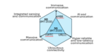
The development of 6G is guided in part by the International Telecommunication Union through its IMT 2030 framework. This framework outlines performance expectations that extend beyond traditional metrics such as throughput and latency. Future networks are expected to integrate sensing and communication, embed artificial intelligence deeply into their operation, and provide seamless connectivity across terrestrial and non terrestrial domains. In parallel, industry groups such as the Third Generation Partnership Project are preparing study items and future specifications that will eventually formalize these goals into implementable standards. Yet standards alone cannot create a new generation of wireless systems. The feasibility of 6G depends on the capabilities of semiconductor technologies that must support higher frequencies, wider bandwidths, and tighter integration than ever before.
One of the most visible shifts in 6G research is the exploration of new spectrum regions, including upper millimeter wave and sub terahertz bands. These frequencies promise extremely wide channel bandwidths and unprecedented peak data rates. However, operating above one hundred gigahertz introduces formidable challenges. Signal attenuation increases, power amplifier efficiency declines, and maintaining linearity becomes more difficult. Thermal constraints intensify as devices attempt to deliver greater output power in compact form factors. In this regime, the physical properties of semiconductor materials, device geometries, and packaging techniques become decisive factors in system performance.
Massive antenna arrays and advanced beamforming further amplify the demands placed on microelectronics. Future base stations and terminals may rely on dense phased arrays that require precise timing, calibration, and mixed signal processing. Each antenna element must be supported by radio frequency circuitry and data converters capable of handling wide instantaneous bandwidths. As arrays grow larger, integration density and power efficiency become critical. The burden on silicon is not only to process signals but to do so within strict energy budgets that align with sustainability goals and practical deployment constraints.
Another defining feature of 6G is the integration of artificial intelligence into network operation. Rather than treating intelligence as an overlay, future systems are expected to incorporate learning and optimization directly into the air interface, resource management, and service orchestration layers. This shift increases the need for specialized accelerators and efficient digital processing units at the edge of the network. Delivering high compute performance per watt will require careful co design of logic, memory, and radio frequency components. Heterogeneous integration techniques that combine complementary semiconductor processes within a single package are likely to play a central role.
Advanced packaging is emerging as a key enabler rather than a secondary consideration. At very high frequencies, interconnect parasitics and package losses can significantly degrade signal integrity. Shortening signal paths through two and three dimensional integration can reduce these effects while enabling tighter coupling between antennas and radio circuitry. By combining silicon based logic with silicon germanium or compound semiconductor devices optimized for high frequency operation, designers can exploit the strengths of multiple technologies within one system.
Bottom line: The journey to 6G will be shaped by the pace of innovation in microelectronics research and development. Achieving the goals envisioned for IMT 2030 requires more than incremental improvements. It calls for breakthroughs in device efficiency, converter performance, thermal management, and system integration. As the industry moves from conceptual studies to formal specifications, the collaboration between standards experts and semiconductor engineers will be essential. Only by aligning ambitious performance targets with the realities of physics and manufacturing can 6G evolve from aspiration to deployment, delivering networks that are not only faster but also more intelligent, reliable, and deeply integrated into the fabric of society.
For more detailed information about the importance of microelectronics in 5G/6G and Alphacore’s role in this development, download the whitepapers “Microelectronics Paving the Way for 6G” and “ML in Microelectronics”. Please also feel free to explore analog, mixed signal and RF solutions on Alphacore’s website https://alphacoreinc.com/
References terms:
- Massive Machine Type Communications (mMTC) is a 5G technology designed to support connectivity for billions of IoT devices.
- Integrated Sensing and Communication (ISAC) is a cornerstone 6G technology that merges wireless communication with radar-like sensing, allowing network infrastructure to detect, track, and image objects in real-time.
- Enhanced Mobile Broadband (eMBB) for centric private networks are tailored 5G deployments designed specifically to provide high-speed, high-capacity connectivity within a defined, private area.
- SMART: Scalable Modular Architecture for RF Transceivers
Also Read:
A Tour of Advanced Data Conversion with Alphacore
Analog to Digital Converter Circuits for Communications, AI and Automotive