You are currently viewing SemiWiki as a guest which gives you limited access to the site. To view blog comments and experience other SemiWiki features you must be a registered member. Registration is fast, simple, and absolutely free so please, join our community today!
I am a fan of product releases which bundle together multiple high-value advances. That approach reduces the frequency of releases (no bad thing) in exchange for more to offer per release, better proven through solid partner validation. The Dynamic Duo III release falls in this class, offering improvements in performance, capacity, and solution support across this matched set of hardware-assisted verification engines (Palladium for emulation and Protium for prototyping).
Capacity and performance advances
It’s a very worn marketing cliché but still true that design sizes keep growing hence the tools to support verification must continue to grow with them. The new generation Palladium Z3 and Protium X3 systems have increased total supported capacity, to 48 billion usable gates and each offer a 50% boost in performance. The Palladium platform is based on a new generation of the Cadence custom emulation processor and the Protium platform is based on the recently released AMD VP1902 device.
Compile times have improved dramatically on large designs through a new modular compiler, delivering near constant compile times independent of design size. For Palladium this maxes out at 8 hours per compile, making 1-2 verification turns per day a reality in early-stage system verification runs. Protium compile times have also dropped, to under 24 hours, speeding prototyping turns in late-stage hardware/firmware validation. Naturally the signature tight coupling between platforms continues with Z3 and X3, allowing for example a run exhibiting a bug in X3 prototyping to be flipped over to Z3 emulation for detailed debug drill-down.
Both platforms continue to deliver form factor and power optimization suitable to enterprise resources, allowing for maximum utilization whether verifying IP, subsystem/chiplet, or full system scale while packing as many jobs as will fit into available resource given job sizes. Both are also available as cloud-based resources.
Since Nvidia has been a long-time fan, I have to believe hardware development for LLMs is among leading drivers motivating these improvements.
Solution apps
Bigger and faster are always important but what really caught my attention in this release are the apps. First, Cadence have spun a new power estimation/analysis app (DPA 3.0), claiming 95% accuracy compared to implementation-level static power analysis (the pre-silicon power signoff of record). Not a new capability of course but sounds like it is much improved and of course running on a platform which can run very big designs with serious use-cases, always important when teasing out power bugs in big systems.
The 4-state emulation app is particularly interesting. Samsung presented a paper at DVCon this year on how they use this capability (currently unique to Palladium apparently) for low power debug. As an example, when switching power states, there are numerous opportunities for bugs to arise around incorrectly enabled isolation logic. X-propagation tests are a good way to catch such bugs but classic X-prop verification using simulation or formal is limited to relatively small design and test sizes. Emulation has the necessary capacity and speed but has historically only supported 0/1 modeling. Now Palladium Z3 also supports 0/1/X/Z as an option, making X-prop testing a very real option on big designs and tests. Samsung were able to show 100X performance improvement in this analysis over a simulation-based equivalent.
In mixed signal emulation, ADI presented an award-winning poster at the same DVCon on their use of the new Palladium app for digital mixed signal (DMS). I believe DMS emulation will become a must-have for 5G, 6G and beyond, to verify correctness between RF and digital stages as software-dependent coupling between stages increases. ADI say their testing shows the methodology is ready for production use, with some limitations and workarounds. Not surprising when forging a new frontier.
The Palladium safety app brings fault simulation to emulation – now we can talk about fault emulation 😀. Michael Young (Sr. Product Management Group Director, Cadence) tells me that speedup versus heavily parallelized software-based fault sim is typically 10-100X. He adds that a common use model is to do most of the relatively short sims using the software platform and to port longer analyses (1 hour or more) to the emulator. The Xcelium safety app and the Palladium share the same fault campaign model so switching between platforms should be simple.
Good fundamentals and good new features in this release. You can read more HERE.
Khaled Maalej is founder and CEO of VSORA, a provider of high-performance silicon chips for GenerativeAI and L4/L5 autonomous driving (AD) applications based in France. Before founding VSORA in 2015, Maalej was CTO at DiBcom, a fabless semiconductor company that designed chipsets for low-power mobile TV and radio reception acquired by Parrot. He graduated from Ecole Polytechnique & Ecole Nationale Superieure des Telecommunications in Paris.
Tell us about your company.
Drawing on more than a decade of expertise in chip architecture initially refined targeting DSP applications in radio communications, VSORA envisioned a processor architecture aimed at delivering exceptional performance with superior efficiency. In today’s computing landscape, while leading processors boast significant computing power, they falter in efficiency, particularly as software workload expands.
We were successful and caught the attention of The Linley Group (now TechInsights). In 2021, our AD1028 architecture clinched the prestigious 2020 Linley Group Analysts’ Choice Awards for Best IP processor.
Over the past two years, we fine-tuned our foundational architecture and created an on-the-fly scalable and reprogrammable computing core. It can perform AI and general-purpose computing or other functionality to target two pivotal and demanding domains through two distinct families of devices. The Tyr family comprises three scalable devices designed to execute the perception and motion planning tasks in L4 (highly automated) and L5 (fully automated) autonomous driving (AD) controllers. The Jotunn family features two scalable devices tailored to meet the demanding generative AI (GenAI) applications.
Save for actual silicon, we have simulated our processors at different abstraction levels all the way into FPGAs via Amazon AWS. Across the board, the results showcase unparalleled processing power (6 petaflops), computing efficiency (50% on GPT-4), minimal latency, restricted energy consumption (40 watt per petaflops), and small silicon footprint.
What problems are you solving?
About a decade ago, Marc Andreessen authored an article titled “Why software is eating the world.” Today, we might assert that the software is eating the hardware. The relentless pursuit of higher processing power by applications such as autonomous driving and generative AI remain unquenchable. While CPUs, GPUs, FPGAs strive to bridge the gap, they fall short of meeting the demands of cutting-edge applications.
What’s needed is a revolutionary architecture capable of delivering multiple petaflops with efficiencies surpassing 50%, while consuming less than 50 watts per petaflops, boasting minimal latencies, and selling at competitive pricing.
That is the challenge that VSORA aims to tackle head-on.
What was the most exciting high point of 2023 for your company?
2023 marked a turning point for VSORA as we achieved a significant milestone. Out of 648 applicants, we were chosen as one of 47 startups to benefit from the 2023 European Innovation Council (EIC) Accelerator Program. This annual event represents a beacon of innovation within the entrepreneurial ecosystem. The selection validates our vision and rewards our efforts with a combination of grants and equity investments to fuel our growth.
What was the biggest challenge your company faced in 2023?
Our goal is to tape our architecture onto silicon. This endeavor requires a substantial investment of up to $50M. In 2023, apart from securing the EIC grant and investment equity, we worked with several VC firms, investment funds, and banks and are optimistic that our efforts will yield fruitful results in 2024.
What do you think the biggest growth area for 2024 will be, and why?
The exponential success of Nvidia underscores the unstoppable ascent of GenAI. Nvidia dominates the learning phase of AI applications executed in large data centers around the world. However, GPUs prove inefficient for edge inference. To mitigate this inefficiency when running ChatGPT-4, extensive arrays of GPUs must be deployed, resulting in exorbitant energy consumption and substantial latency issues. This setup not only entails significant acquisition costs but also proves expensive to maintain and operate.
Another promising area for growth lies in AD. Over the past three to four years, the push to implement level 4 and 5 AD controllers has somewhat lost intensity, primarily due to the absence of viable solutions in the market. We anticipate a resurgence of momentum in 2024, fueled by a better understanding of the requisite specifications and the emergence of advanced digital processing capabilities.
How does your company address this growth?
In advanced algorithms like transformers, relying solely on pure AI instructions is no longer adequate. Consider the PointPillars algorithm, which incorporates pure AI functions and DSP functions within its code. Or in the case of Mask R-CNN that mixes general processor instructions and pure AI functions. At VSORA, we integrate MAC and ALU functions within our compute cores, and transfer data with a high-bandwidth, on-chip memory system through a proprietary scheme engineered to overcome the challenges posed by “memory wall.”
Moreover, we enable layer-by-layer specific any-bit floating point quantization and support sparsity both in weights and data on-the-fly. The approach frees developers from dealing with code details by automatically determining the optimal configuration for each task.
The tangible results of these innovations are evidenced in the specifications for Jotunn.
What new features/technology are you working on?
We believe our hardware architecture is robust and performing. We are now focusing on enhancing our software capabilities.
Our newly developed software offers a distinct advantage over competitors. Unlike solutions based on CUDA-like, low-level programming languages where developers must specify loops for matrix multiplication, VSORA operates at the algorithmic level (Matlab-like, Tensorflow-like, C++) avoiding the need to engage in low-level programming and optimization that may demand significant vendor attention. The VSORA software environment shields users from dealing with these lower-level intricacies, enabling them to focus solely on the algorithms.
As for algorithms validation, the VSORA development environment encompasses a suite of simulation tools to verify code at high-level, transaction-level-modeling (TLM) and register transfer level (RTL) model, as well as on AWS FPGAs.
How do customers engage with your company?
First contact might be through our website (VSORA.COM), and I encourage readers to visit it. We can always be reached via email at info@vsora.com.
Dan is joined by Bill DeVries, Vice President of Industry Transformation and Customer Success at Dassault Systémes. Bill is responsible for revenue growth and driving the use of the 3DEXPERIENCE platform. Additionally, Bill is the Senior Director of Academic and Education in North America, where he leads the 3DEXPERIENCE EDU Sales and Workforce of the Future efforts by working closely with prominent Universities, Colleges and technical institutions.
Dan explores some of the ways Dassault Systémes is impacting workforce development with Bill. During this broad discussion, Bill describes some of the partnerships Dassault Systémes has with entities such as Purdue University and Lam Research. Using a technology called virtual twin, a complete design and manufacturing environment can be created virtually to facilitate the development of new skills in both design and semiconductor fabrication. The technology is also quite useful for commercial customers who would like to optimize workflows.
Bill discusses the CHIPS Act and how this work will help to develop the significant number of new skills required to staff the new facilities that are planned. Bill also describes how expanded ecosystem collaboration will help to create the workforce of the future.
The views, thoughts, and opinions expressed in these podcasts belong solely to the speaker, and not to the speaker’s employer, organization, committee or any other group or individual.
Soitec is a unique company that is at the center of major changes in our industry. Technology megatrends are fueling massive demand for semiconductors and this has increased the adoption of engineered substrates. As a global leader in the development of engineered substrates, Soitec is a company to watch. While this technology finds use across many areas of semiconductor application, photonics is a particularly important area that is enabled by Soitec and its engineered substrates. The company recently published a very informative white paper on the topic. A link is coming so you can get your own copy. First, let’s explore a bit about the company and its strategy to see how Soitec delivers the foundation for next-generation interconnects.
About Soitec
With the demands of density, performance and power efficiency required for advanced semiconductors, it turns out that silicon in its purest form often falls short to deliver on all the requirements. Adding additional materials to the silicon can enhance its capabilities, but adding an epitaxial layer of new material to silicon can be both difficult and unpredictable. Soitec has developed a process to deliver engineered substrates that addresses these challenges, opening new opportunities for innovation. You can learn about some of the things Soitec is doing here.
Thanks to the increasing adoption of engineered substrates, the company expects its addressable market to grow by 3X between 2022 and 2030. The breadth of Soitec’s impact is illustrated in the figure below.
Soitec’s impact
About Photonics
As with many trends, AI/ML is a main driver for photonics adoption. The current infrastructure for these applications is bandwidth and distance limited. A move to optical interconnect is on the horizon that will open new possibilities. The figure below summarizes these trends.
AI Enablement as a Network Solution
To address these opportunities, Soitec has a roadmap that is summarized below.
Smart Photonics SOI Roadmap
With this backdrop, I’ll provide a summary of the new white paper.
About the White Paper
The new white paper is appropriately titled, Has Silicon Photonics Finally Found It’s Killer Application? The piece explains how engineered silicon substrates are providing the foundation for the cutting-edge photonics engines that data centers will need to usher in the era of artificial intelligence.
The piece talks about the onset of artificial intelligence and machine learning that leverage large language models (LLMs) for both AI training and inference. These models exhibit a super-exponential growth in modeling parameters. As a result, inter-data and especially intra-data center traffic has exploded, requiring the need for high-speed optical pluggable transceivers. These devices are currently transitioning from 100 Gbps to 400 Gbps. Some shipments of 800-Gbps devices already started in 2023 and even 1.6-Tbps pluggables are also available today for pre-sampling.
The piece goes on to explain that optical transceivers must address three different key requirements: high speed, low power, and minimized cost. Regarding power, server clusters in a data center deliver power densities between 50 and 100 kW to meet new AI requirements. However, the share of AI workloads in a data center is expected to more than double between 2023 and 2028. How these trends impact power consumption is illustrated in the table below.
Data Center Power Consumption Trends
This means there is a significant need for lower-power, higher-speed optical transceivers as data volume grows, which is driving pluggable form factors to evolve. The piece points out that the digital signal processing (DSP) chip inside pluggable transceivers is one of the main sources of power consumption. This has led to exploration of novel transceiver designs, such as linear-drive pluggable optics (LPOs), half-retimed linear optics (HALOs), and co-packaged optics (CPOs), that use advanced device design and photonics-electronics co-integration. This would enable future pluggables to operate in direct-drive, without a stand-alone, dedicated DSP component.
The figure below illustrates this evolution.
Evolution of Optical Interconnect
The white paper then discusses the changes on the horizon to optimize power, performance and cost of AI architectures, with a focus on transceiver design. As shown earlier, silicon photonics will play a major role in these changes. And silicon-on-insulator technology has unique properties to address the demanding requirements of silicon photonics.
The details of Soitec’s engineered substrates to address these requirements is presented in detail. There is a lot of great information presented – you should get a copy of this white paper. A link is coming.
The Executive Viewpoint
René Jonker
René Jonker has recently been named as the SVP & GM of Smart Devices Division at Soitec. He oversees Imager, FD-SOI for IoT applications and silicon photonics. I had the opportunity to speak with René recently to get his view of the trends regarding silicon photonics and Soitec’s position in this growing market.
René began by discussing the mega-trends that are creating the disruption we are currently seeing. He cited the growth in size and scale of data centers and the associated increased demand for bandwidth as important drivers. He also mentioned the power consumption that comes along with these changes; this was a big topic at the recent OFC Conference in San Francisco.
He commented that electrical interconnects will still have a place – primarily in server backplanes where the technology can deliver cost-effective performance. From a system perspective, he felt that photonics and optical interconnects are really the only technology to address the previously mentioned demands and manage power consumption at the same time. René mentioned the discussion of 1.6T and 3.2T deployments at OFC; the world of interconnects is clearly changing in performance and implementation approach as these levels are simply not possible in the electrical domain.
René then discussed implementation approaches for optical interconnect. He pointed out that silicon photonics is a main focus today, primarily because of the familiarity the entire supply chain has with silicon devices. He explained that as system demands increase, modified substrates play a key role to unlock next-generation performance to deliver on key parameters such as insertion loss. He went on to explain that the uniformity of these substrates is critical to deliver high yielding, high performance devices. The surface smoothness and robustness of the substrate are also critical. These are areas where Soitec has a very strong position.
He explained that Soitec’s product roadmap is delivering advanced capabilities for both 200mm and 300mm wafers (see roadmap diagram above). We then talked about the drivers for all the bandwidth requirements, and simply put AI/ML is the main driver, both inference and training. René discussed co-packaged optics as a way to bring the networking layer closer to the processor to reduce loss/power and increase bandwidth. With regard to new materials, he mentioned thin film lithium niobate as one promising approach, there are others.
We concluded our discission by observing that Soitec is at the epicenter of trends like new substrates and co-packaged optics thanks to its engineered substrate technology and experience. I summarized the position of the company as “right place, right time”.
As a final question, I asked René when we could see substantial changes in optical interconnect deployments begin to take hold. He was quick to point out he didn’t have a crystal ball, but he felt 2027/2028 would be an exciting time. This is right around the corner.
To Learn More
It appears that silicon photonics will have a major impact on many new systems going forward. Soitec is a key player in this emerging market and the recent white paper will give you great insight into the relevant trends and opportunities. I highly recommend getting a copy. The white paper is part of the March edition of PHOTONICS spectra magazine. You can get your copy here. The white paper begins on page 38. And that’s how Soitec delivers the foundation for next-generation interconnects.
The goal of SoC design teams is to tape-out their project and receive working silicon on the first try, without discovering any bugs in silicon. To achieve this lofty goal requires all types of specialized checking and verification during the design phase to prevent bugs. There are checks at the system level, RTL level, gate level, transistor level and physical layout levels. One newer EDA company is Aniah, and their focus is on checking the correctness of IC designs at the transistor level through Electrical Rule Checking (ERC) by employing formal methods and smart clustering of errors
During ERC a formal tool can mistakenly report “false positives”, and these are false errors that shouldn’t have been reported. Real design errors that are not detected are called “false negatives”, so the ideal formal tool has zero false negatives. The Aniah formal ERC tool is called OneCheck, and I’ve just read their White Paper to get up to speed on how it works.
The Aniah OneCheck ERC can be run on a design in several places for IC flows to verify both analog and digital circuitry:
Aniah Tool Flow
Some common design flaws caught by formal checkers include:
Missing Level Shifters
Floating Gates
High Impedance states
Floating Bulk
Diode Leakage
Electrical Overstress
False Errors
There are four typical classes of false errors that an ERC tool can be fooled by, so the following examples illustrate the challenges.
1. Topology Specific
The following circuit has two power domains – VDD, Vin; a level shifter is expected between them, and here the false error flags transistors M2 and M3, because their gates are connected to net A and Net 1 which are powered by Vin, not VDD. Transistors M0 and M1 actually control the “1” level.
False Error: Missing Level Shifter
2. Analog Path
A differential amplifier has devices M1 and M2 that are biased to act as an amplifier with current provided by M3, yet a false error reports an analog path issue.
False Error – analog path
3. Impossible Path Logically
An inverter of M1, M2 is driven by a lower range signal. When net 3 is ‘1’, then M2 pulls down output net 2 to a ‘0’, but the false error reports a logic path through M3 and M1.
False Error – Impossible path
4. Missing supply in setup
When a ring oscillator circuit requires a regulated supply value of 1.2V, but the regulator has a supply value of 2.5V, then a false error can be reported for electrical overstress.
False Error – Missing supply in setup
OneCheck
The good news is that OneCheck from Aniah has a smart Clustering Root-Cause analysis methodology to handle these four types of false errors. This formal circuit checker doesn’t use any vectors because all circuit states are verified in just one run, which includes verification of all power states of each circuit. Commercial circuits on mature or latest generation nodes have been run through OneCheck, so it’s a reliable tool.
Your circuit design team can start using OneCheck after the first schematic netlists are entered, even before any simulations have been run. The actual run times of OneCheck are quite fast, typically just a few seconds on a mixed-signal designs with over 10 million transistors and more than 10,000 different power scenarios.
1. Topology Specific
OneCheck detects topology-related false errors like missing level shifters by performing pseudo-electrical analysis to model voltages and currents.
2. Analog Path
With Aniah OneCheck a user can identify and filter false errors with any current or voltage reference net.
3. Impossible path logically
The OneCheck tool finds all tree-like paths used by analog multiplexors, and the user can reject thousands of false errors quickly.
4. Missing supply in setup
All errors corresponding to a missing supply are clustered together, so users can easily update the power supply setup.
Summary
Finding circuit bugs before manufacturing is the preferred method to ensure first silicon success, so ERC is another tool for chip design teams to use. Other ERC tools report way too many false errors, so that his limited their acceptance in the design community. Aniah has delivered new formal technology to combat this issue of false errors for ERC.
Why not give OneCheck a try on some of your biggest IC designs, as the evaluation process is free and easy.
Read the full 11-page White Paper fromAniah online.
The relentless pursuit for maximizing performance in semiconductor development is now matched by the crucial need to minimize energy consumption.
Traditional simulation-based power analysis methods face insurmountable challenges to accurately capture complex designs activities in real-world scenarios. As the scale of modern SoC designs explodes, a new pre-silicon dynamic power analysis methodology is essential. This approach should center on executing representative real-world software workloads.
Power Consumption: Static vs Dynamic Power Analysis
Two primary factors contribute to energy dissipation in semiconductors: static power consumption and dynamic power dissipation. While both are grounded in physics concerning dimensions, voltages, currents, and parasitic elements (resistance and capacitance, or RC), static power consumption remains largely unaffected by the type and duration of the software workload, except for power management firmware that shuts down power islands. Conversely, dynamic power dissipation is heavily dependent on these workload attributes.
Understanding that the dynamic power dissipated by a circuit scales with the logical transitions occurring during its operation, it becomes crucial to accurately capture its switching activity in order to achieve precise power analysis and optimize power dissipation for a design.
Average And Peak Power Analysis
Recording the switching activity as toggle count data, without correlating it with corresponding time intervals, restricts the analysis to average power consumption over the operational time window. Typically, the switching data is cumulatively recorded throughout an entire run in a file format called the switching activity interchange format (SAIF). The size of the SAIF file remains constant irrespective of the duration of the run but grows with the design complexity (i.e. the number of nets in the design).
Capturing time-based and cycle-by-cycle information, namely, full activity waveforms, allows for calculating power consumption as a function of time during device operation. Signal transitions along their associated timestamps are typically recorded for the entire run in a signal database, traditionally stored in the industry standard FSDB (Fast Signal DataBase) format. Today this format is no longer adequate due to the considerable size of the switching file, which escalates with longer runs, potentially reaching terabytes for extended runs spanning billions of cycles. More efficient methods utilize the native output format directly provided by the emulator.
Accurate Power Analysis: Design Hierarchy Dependency
The accuracy of the switching activity is contingent upon the level of design details accessible during the recording session. As the design description evolves from high level of abstraction in the early stages of the development to the Register Transfer level (RTL), gate level and, eventually, down to the transistor level, increasingly detailed design information becomes accessible.
The accuracy of power estimation varies across different levels of abstraction in semiconductor design. At the transistor level, the accuracy is typically within 1% of the actual power dissipation of the silicon chip. This decreases to approximately 2 to 5% at the gate level, around 15 to 20% at the RTL (Register Transfer Level), and ranges from 20% to 30% at the architectural level. However, higher levels of abstraction offer faster turnaround time (TAT) and empower designers to make influential decisions that affect power consumption.
The accuracy vs. TAT tradeoff poses a challenge to designers., At the architectural level, designers enjoy the greatest flexibility to compare multiple architectures, explore various design scenarios, perform power trade-offs, and achieve optimal power optimizations. Instead, at the gate level where accuracy is higher, there is limited flexibility for significant optimizations beyond marginal improvement. The RTL strikes the optimal compromise, providing sufficient details for accurate power consumption analysis while retaining enough flexibility for substantial power optimizations. Moreover, it’s at the RTL where software and hardware converge in the design flow for the first time, enabling engineers to explore optimizations in both domains. Software drivers, in particular, can profoundly impact the power characteristics of the overall design.
Accurate Power Analysis: Design Activity Dependency
Dynamic power consumption depends heavily on the design activity, which can be stimulated using various techniques. These may include external stimuli applied to its primary inputs or the execution of software workloads by embedded processors within the device under test (DUT). Software workloads encompass booting an operating system, executing drivers, running entire applications such as computationally intensive industry benchmarks, and performing tests/diagnostics.
According to Tom’s Hardware, the improvements to idle power usage on Radeon RX 7800 XT and 7700 XT GPUs are massive – with the 7800 XT dropping from 33W to 12.9W and the 7700 XT dropping from 27.5W to 12W.[1]
Stimulus in the form of synthetic tests as used in functional verification testbenches fail to exercise the design to the extent necessary to toggle most of its fabric. This level of activation can only be achieved through the execution of realistic workloads.
Meeting Dynamic Power Analysis Challenges with Hardware Emulation
Verification engines such as software simulators, while effective for recording switching activity, are limited by execution speed, greatly dependent on design size and stimulus duration. Attempting to boot Android OS via an HDL simulator may take years, rendering it unfeasible.
To overcome these limitations and still capture detailed toggle data, hardware emulators emerge as the superior choice. They can complete such demanding tasks within a reasonable timeframe.
Hardware emulators operate at six or more orders of magnitude faster than logic simulators. However, executing even a few seconds of real-time operations on an emulated design can amount to billions of cycles, taking several hours at emulation speed of few megahertz.
Rather than relying solely on sheer computational power, adopting a divide and conquer approach proves to be more effective and efficient. The primary objective remains ensuring that both the average and peak power consumption levels adhere to the specified power budget outlined in the design requirements. In the event of a breach of the power budget, it is essential to swiftly and easily identify the underlying cause.
Performing Power Analysis with a Three-Step Methodology
A best-in-class hardware emulator can accomplish the task in three steps. See figure 1.
Figure 1: Finding Power Issues in Billion Cycles Workloads (Source: Synopsys)
Step One
In step one, a power model based on the RTL design is generated and executed on the emulator for the entire run of multi-billion cycles. The emulator conducts activity-based calculations and produces a weighted activity profile (WAP), i.e., a time-based graph that is a proxy for power. See example in figure 2.
Figure 2: Weighted-activity profile showing a power bug. (Source: Synopsys)
By visually inspecting the WAP, users can identify areas of interest for analysis, pinpointing time windows of few million cycles with exceedingly high activity, which may indicate opportunities for optimization or reveal potential power bugs.
Step Two
In step two, the emulator runs through that time window of few million cycles and genrates a signal activity database. Subsequently, a special-purpose massively parallel power analysis engine is used to compute power and generate the power waveform. Worth mentioning, a “save&restore” capability may accelerate the process by resuming from the closest checkpoint to the time window under investigation. In this step, a fast power calculation engine is required to achieve turn-around times of less than a day for tens of millions of cycles. Its accuracy should falls in the range of 3% to 5% of power signoff analysis to facilitate informed decision-making regarding actual power issues. Additionally, a secondary inspection of the power profile graph within the few million cycles time window aids users to pinpoint a narrower time window of few thousands cycles around the power issue.
Step Three
In the final step 3, the emulator processes the narrower time window of few thousands cycles and generates an FSDB waveform database to be fed to into a power sign-off tool to output highly accurate average and peak power data.
In each successive step, users progressively zoom in by approximately a factor of a thousand, narrowing down from billions to millions, and finally down to thousands of cycle ranges.
The three-step process allows for the discovery of elusive power issues, akin to finding the proverbial needle in the haystack.
Taking it further: Power Regression
The fast execution speed of leading-edge hardware emulators and massively parallel power analysis engines enable efficient power regression testing with real-world workloads. This capability greatly enhances pre-silicon verification/validation by promptly identifying and removing power-related issues before they manifest in silicon.
Typically, each new netlist release of a DUT can undergo rapid assessment to certify compliance with power budgets. Running power regressions on a regular basis ensure consistent achievement of power targets.
Viewing inside: Virtual Power Scope
Performing post-silicon power testing on a lab testbench presents challenges because of limited visibility into the design. Despite operating at gigahertz speeds, test equipment typically samples power data at a much lower rate, often in the kilohertz range. This results in sparse power measurements, capturing only one power value per million cycles. Moreover, unless the chip was specifically designed with separate supply pins per block, obtaining block-by-block power data via silicon measurements proves exceedingly difficult. Frequently, only a chip-level power trace is available.
Pre-silicon power validation conducted through hardware emulation and massively parallel power analysis acts as a virtual power scope. It enables tracing and measurement of power throughout the design hierarchy, ensuring adherence to target specifications. This analysis can delve down to the individual cell level, accurately evaluating the power consumption of each block and component within the design. Essentially, it functions akin to a silicon scope, providing insight into the distribution of power within the chip.
Expanding beyond lab analysis: IR Drop Testing
The ability to compute power on a per-cycle basis makes it possible to detect narrow windows, spanning 10 or 20 cycles, where sudden power spikes may occur. Such occurrences often elude detection in a lab environment.
These intervals can undergo analysis using IR (where I is current and R is resistance) drop tools. These tools assess IR drop across the entire SoC within a range typically spanning 10 to 50 cycles of switching activity data.
Achieving optimization sooner, with greater precision: SW Optimization
By aligning the software view of the code running on a processor core with a power graph, it becomes feasible to debug hardware and software concurrently using waveforms.
The connection between these tools is the C debugger operating on a post-emulation trace against a set of waveform dumps. Although these waveform dumps are generated by the emulator, they can encompass various types of waveforms, including those related to power.
Conclusion
Accurately analyzing dynamic power consumption in modern SoC chips at every development stage is crucial. This proactive approach ensures adherence to the power consumption standards of the intended target device, thereby averting costly re-spins.
To achieve realistic results and avoid potential power issues, the DUT, potentially encompassing billions of gates, must undergo testing with real-world software workloads that require billions of cycles. This formidable task is achievable solely through hardware emulation and massively parallel power analysis.
—
SIDEBAR
The methodology presented in this article has been successfully deployed by SiMa.ai, an IDC innovation startup for AI/ML at the edge. SiMa.ai used the Synopsys’ ZeBu emulation and ZeBu Empower power analysis solution.
Lauro Rizzatti has over three decades of experience within the Electronic Design Automation (EDA) and Automatic Test Equipment (ATE) industries on a global scale. His roles encompass product marketing, technical marketing, and engineering, including management positions. Presently, Rizzatti serves as a hardware-assisted verification (HAV) consultant. Rizzatti has published numerous articles and technical papers in industry publications. He holds a doctorate in Electronic Engineering from the Universita` degli Studi di Trieste in Italy.
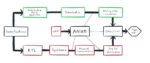
Semidynamics takes a non-traditional approach to design enablement. Not long ago, the company’s Founder and CEO, Roger Espasa unveiled extreme customization at the RISC-V Summit. That announcement focused on a RISC-V Tensor Unit designed for ultra-fast AI solutions. Recently, at Embedded World 2024 the company took this strategy a step further with an All-In-One AI IP processing element. Let’s look at the challenges addressed by this new IP to understand how Semidynamics shakes up Embedded World 2024 with All-In-One AI IP to power nextgen AI chips.
The Problem
The current approach to AI chip design is to integrate separate IP blocks next to the system CPU to handle the ever-increasing demands of AI. As data volume and processing demands of AI increase, more individual functional blocks are integrated. The CPU distributes dedicated partial workloads to gpGPUs (general purpose Graphical Processor Units) and NPUs (Neural Processor Units). It also manages the communication between these units.
Moving data between the blocks this way causes high latency. Programming is also challenging since there are three different types of IP blocks with different instruction sets and tool chains. It is also worth noting that fixed-function NPU blocks can become obsolete quickly due to constant changes in AI algorithms. Software evolves faster than hardware.
The figure below illustrates what a typical AI-focused SoC looks like today.
Typical AI Focused SoC today
The Semidynamics Solution
Semidynamics has taken a completely different approach to AI chip design. The company has combined four of its IPs together to form one, fully integrated solution dubbed the All-In-One AI IP processing element. The approach delivers a fully customizable RISC-V 64-bit core, Vector Units (as the gpGPUs), and a Tensor Units (as the NPUs). Semidynamics Gazzillion® technology ensures huge amounts of data can be handled without the issues of cache misses. You can learn more about Gazillion here.
This approach delivers one IP supplier, one RISC-V instruction set and one tool chain making implementation easier and faster with lower risk. The approach is scalable, allowing as many new processing elements as required to be integrated on a single chip. The result is easier access to next generation, ultra-powerful AI chips.
The figure below illustrates this new approach of fusing CPU, gpGPU, and NPU.
Fusing CPU, gpGPU, and NPU
This approach goes well beyond what was announced at the RISC-V Summit. A powerful 64-bit out-of-order based RISC-V CPU is combined with a 64-bit in-order based RISC-V CPU, a vector unit and a tensor unit. This delivers powerful AI capable compute building blocks. Hypervisor support is enabled for containerization and crypto is enabled for security and privacy. And Gazzillion technology efficiently manages large date sets
The result is a system that is easy to program with high-performance for parallel codes and zero communication latency.
The technology is available today with a straight-forward business model as shown below.
Flexible and Customizable Business Model
Comments from the CEO
Roger Espasa
Recently, I was able to get a few questions answered by Roger Espasa, the founder and CEO of Semidynamics.
Q: It seems like integration is the innovation here. If it’s easy, why has it not been done before?
A: It is a paradigm change – the starting RISC-V momentum was focussed solely on CPU, both in the RISC-V community and with the customers. We have seen vector benefits way earlier than others and AI very recently demands more flexible response to things like transformers and LLMs. In fact, it’s far from easy. That’s why it’s not been done before. Especially as there was no consistent instruction set in one environment until CPU+Vector and the Semidynamics Tensor from our prior announcement.
Q: What were the key innovations you needed to achieve to make this happen?
A: I’ll start with eliminating the horribly-difficult-to-program DMAs typical of other NPU solutions and substituting their function by normal loads and stores inside a RISC-V core that get the same sustained performance – actually better. That particular capability is only available in Semidynamic’s RISC-V cores with Gazzillion technology. Instead of a nasty DMA, with our solution the software only needs to do regular RISC-V instructions for moving data (vector loads and stores, to be precise) into the tensor unit.
Also, connecting the tensor unit to the existing vector unit, where the vector register storage is used to hold tensor data. This reduces area and data duplication, enables a lower power implementation, and, again, makes the solution easier to be programmed. Now, firing the tensor unit is very simple: instead of a complicated sequence of AXI commands, it’s just a vanilla RISC-V instruction (called vmxmacc, short for “matrix-multiply-accumulate“). Adding to this, AXI commands mean that the CPU has to read the NPU data and either slowly process it by itself or send it over AXI to, for example, a gpGPU to continue calculations there.
And adding specific vector load instructions that are well suited to the type of “tiled” data used in AI convolutions and can take advantage of our underlying Gazzillion technology.
I should mention that this result can only be done by an IP provider that happens to have (1) a high-bandwidth RISC-V core, (2) a very good vector unit and (3) a tensor unit and can propose new instructions to tie all three solutions together. And that IP provider is Semidynamics!
The resulting vision is a “unified compute element” that:
1) Can be scaled up by simple replication to reach the customer TOPS target – very much like multi cores are built now. I will offer an interesting observation here: nobody seems to have a concern to have a multicore system where each core is an FPU, but once there is more than one FPU, i.e. a Vector unit, nobody understands it anymore!
2) Keeps a good balance between “control” (the core), “activation performance” (the vector unit) and “convolution performance” (the tensor unit) as the system scales.
3) Is future proofed. By having a completely programmable vector unit within the solution, the customer gets a future-proofed IP. No matter what type of AI gets invented in the near future, the combination of the core+vector+tensor is guaranteed to be able to run it.
Q: What were the key challenges to get to this level of integration?
A: Two come to mind: (1) inventing the right instructions that are simple enough to be integrated into a RISC-V core and, yet provide sufficient performance, and (2) designing a tensor unit that works hand-in-hand with the vector unit. There are many more technical and architectural challenges we solved as well.
To recap: the challenge is that we change the paradigm: we do a modern AI solution that is future proof and based on an open source ISA.
That datacenters are power hogs is not news, especially now AI is further aggravating this challenge. I found a recent proteanTecs-hosted panel on power challenges in datacenter infrastructure quite educational both in quantifying the scale of the problem and in understanding what steps are being taken to slow growth in power consumption. Panelists included Shesha Krishnapur (Intel fellow and IT CTO), Artour Levin (VP, AI silicon engineering at Microsoft). Eddie Ramirez (Arm VP for Go-to-Market in the infrastructure line of business), and Evelyn Landman (Co-founder and CTO at proteanTecs). Mark Potter (VC and previously CTO and Director of HP Labs) moderated. This is an expert group directly responsible for or closely partnered with some of the largest datacenters in the world. What follows is a condensation of key points from all speakers.
Understanding the scale and growth trends
In 2022 US datacenters accounted for 3.5% of total energy consumption in the country. Intel sees 20% compute growth year over year which through improved designs and process technologies is translating into a 10% year over year growth in power consumption.
But that’s for CPU-based workloads. Sasha expects demand from AI-based workloads will grow at twice that rate. One view is that a typical AI-accelerated server is drawing 4X the power of a conventional server. A telling example suggests that AI-based image generation consumes almost 10X the power of just trying to find images online. Not an apples and apples comparison of course but if the AI option is easier and produces more intriguing results, are end-users going to worry about power? AI has the potential to turn an already serious power consumption problem into a crisis.
For cooling/thermal management the default today is still forced air cooling, itself a significant contributor to power consumption. There could be better options but re-engineering existing infrastructure for options like liquid/immersion cooling is a big investment for a large datacenter; changes will move slowly.
Getting back onto a sustainable path
Clearly this trend is not sustainable. There was consensus among panelists that there isn’t a silver bullet fix and that datacenter power usage effectiveness (PUE) must be optimized system-wide through an accumulation of individually small refinements, together adding up to major improvements.
Shesha provided an immediate and intriguing example of improvements he has been driving for years in Intel datacenters worldwide. The default approach, based on mainframe expectations, had required cooling to 64-68oF to maximize performance and reliability. Research from around 2010 suggested improvements in IT infrastructure would allow 78oF as a workable operating temperature. Since then the limit has been pushed up higher still, so that PUEs have dropped from 1.7/1.8 to 1.06 (at which level almost all the power entering the datacenter is used by the IT equipment rather than big cooling systems).
In semiconductor design everyone stressed that power optimization will need to be squeezed through an accumulation of many small improvements. For AI, datacenter inference usage is expected to dominate training usage if AI monetization is going to work. (Side note: this has nothing to do with edge-based inference. Business applications at minimum are likely to remain cloud based.) One way to reduce power in inference is through low-precision models. I wouldn’t be surprised to see other edge AI power optimizations such as sparse matrix handling making their way into datacenters.
Conversely AI can learn to optimize resource allocation and load balancing for varying workloads to reduce net power consumption. Aligning compute and data locations and packing workloads more effectively across servers will allow for more inactive servers which can be powered down at any given time.
Naturally Eddie promoted performance/watt for scale-out workloads; Arm have been very successful in recognizing that one size does not fit all in general-purpose datacenters. Servers designed for high performance compute must coexist with servers for high traffic tasks like video-serving and network/storage traffic optimization. Each tuned for different performance/watt profiles.
Meanwhile immersion and other forms of liquid cooling, once limited to supercomputer systems, are now finding their way into regular datacenters. These methods don’t reduce IT systems power consumption, but they are believed to be more power-efficient in removing heat than traditional cooling methods, allowing for either partial or complete replacement of forced air systems over time.
Further opportunities for optimization
First, a reminder of why proteanTecs is involved in this discussion. They are a very interesting organization providing monitor/control “agent” IPs which can be embedded in a semiconductor design. In mission mode these can be used to supply in-field analytics and actionable insights on performance, power and reliability. Customers can for example use these agents to adaptively optimize voltages for power reduction while not compromising reliability. proteanTecs claim demonstrated 5% to 12% power savings across different applications when using this technology.
Evelyn stressed that such approaches are not only a chip level techonology. The information provided must be processed in datacenter software stacks so that workload optimization solutions can take account of on-chip metrics in balancing between resources and systems. Eddie echoed this point in adding that the more information you have and the more telemetry you can provide the software stack, the better the stack can exploit AI-based power management.
Multi-die systems are another way to reduce power since they bring otherwise separate components closer together, avoiding power-hungry communication through board traces and device pins.
Takeaways
For semiconductor design teams, expect power envelopes to be squeezed more tightly. Since thermal mitigation requirements are closely coupled to power, expect even more work to reduce hotspots. Also expect to add telemetry to hardware and firmware to guide adaptive power adjustments. Anything that affects service level expectations and cooling costs will go under the microscope. Designers may also be borrowing more power reducing design techniques from the edge. AI design teams will be squeezed extra hard 😀 Also expect a bigger emphasis on chiplet-based design.
In software stacks, power management is likely to become more sophisticated for adaptation to changing workloads in resource assignments and power down for systems not currently active.
In racks and the datacenter at large, expect more in-rack or on-chip liquid-based cooling, changing thermal management design and analysis at the package, board and rack level.
Dan is joined by Randy Caplan, co-founder and CEO of Silicon Creations, and a lifelong technology enthusiast. For almost two decades, he has helped grow Silicon Creations into a leading mixed-signal semiconductor IP company with nearly 500 customers spanning almost every major market segment.
Randy provides some background on Silicon Creations unique bootstrapped business model. Today, the company provides critical analog/mixed signal IP to many customers across a wide variety of markets. Silicon Creations has delivered IP in apprixantely 85 process nodes.
Randy explores how the company has succeeded and assesses what its impact will be in the future.
The views, thoughts, and opinions expressed in these podcasts belong solely to the speaker, and not to the speaker’s employer, organization, committee or any other group or individual.
Winner and Runner-up to receive the contest’s largest ever technology credit for production tape-outs.
This is an example of why I enjoy working with Silicon Catalyst. They collaborate with our partners and do some really impressive things, all for the greater good of the semiconductor industry, absolutely. If you are not currently engaged with the Silicon Catalyst ecosystem you need to be.
With the overwhelming success of last year’s contest which resulted in $150,000 in Arm technology credit awarded to the winner, this year the bounty has been increased to $250,000 to the top startup.
The 2024 Arm Flexible Access for Startups Contest is open to privately owned startup companies in pre-seed, seed and Series A funding that have raised a maximum of $20 million in funding. The applicant companies need to either be using Arm or considering using Arm in their products. An Arm technology credit of $250,000 and $150,000, will be awarded to the winner and runner-up, respectively, and can be used towards a commercial tape-out and could cover IP fees for a complete embedded system or contribute to the cost of a higher performance system. Both the winner and runner-up will also receive additional benefits, including a pitch review session hosted by the Silicon Catalyst Angels investment group. All contest applicant organizations will also be considered for acceptance to the Silicon Catalyst Incubator/Accelerator.
Last year’s winner Equal1 is a pioneering silicon quantum computing company dedicated to making quantum computing affordable and accessible:
“We are thrilled to be announced as the winner of the 2023 ‘Silicon Startups Contest’. Arm’s support, partnership, and technology credit are invaluable to the development of our QSoC processors. Just as the evolution of classical computers was driven by advancements in silicon processors, we firmly believe quantum computing will follow the same silicon path. Like the majority of chips today, the new era of quantum computing will be powered by Arm, with a focus on power efficiency, performance, proven reliability, and a robust ecosystem.”
This year, the overall winner receives $250,000 Arm technology credit toward an Arm Flexible Access commercial tape-out. The runner-up receives $150,000 Arm Technology Credit towards an Arm Flexible Access commercial tape-out. The winner and runner-up will also receive:
A free Arm Design Review to enable Arm to review the customer’s design specification, Ticket to Arm’s invite-only ecosystem event for networking and a chance to be featured, and a pitch review session hosted by the Silicon Catalyst Angel investment group.
Additionally, Paul Williamson, Senior Vice President and General Manager, IoT Line of Business at Arm said:
“Arm technology is for everyone, and through this contest, we are recognizing and supporting the next wave of innovators to grow their business and accelerate their SoC designs. We know that time to product and access to the largest possible market are critical for startups, which is why we created Arm Flexible Access for Startups, providing $0 access to a wide portfolio of IP, tools and support, to maximize their chance of success.”
If you remember, we wrote the definitive book on Arm “Mobile Unleashed: The Origin and Evolution of the Arm Processor in our Devices” and we have written hundreds of related Arm articles. This contest is an incredible opportunity to work closely with the #1 processor IP company and the world’s only incubator focused exclusively on accelerating semiconductor solutions.