llmda newsletter ad (2)

Process Design Kits: PDKs, iPDKs, openPDKs

Process Design Kits: PDKs, iPDKs, openPDKs
by Paul McLellan on 03-24-2011 at 5:28 pm

One of the first things that needs to be created when bringing up a new process is the Process Design Kit, or PDK. Years ago, back when I was running the custom IC business line at Cadence, we had a dominant position with the Virtuoso layout editor and so creating a PDK really meant creating a Virtuoso PDK, and it was a fairly straightforward task for those process generations.

The PDK contains descriptions of the basic building blocks of the process: transistors, contacts etc and are expressed algorithmically as PCells so that they automatically adjust depending on their parameters. For example, as a contacted area gets larger, additional contact openings will be created (and perhaps even removed, depending on the design rules).

Two things have changed. Firstly, Virtuoso is no longer the only game in town. All the major EDA companies have their own serious offerings in the custom layout space, plus there are others. But none of these other editors can read a Virtuoso PDK which is based on Cadence’s SKILL language. The second thing that has changed is that design rules are so much more complex that creating the PDK is a significant investment. Creating multiple PDKs for each layout editor is more work still, and work that doesn”t really bring a lot of value to either the foundry or the user.

Since Cadence isn’t about to put its PDKs (and PCells) into the public domain as a standard everyone can use, a new standard was needed. The Interoperable PDK Libraries Alliance (IPL), working with TSMC, standardized on using Ciranova’s PyCell approach (based on Python rather than SKILL) and created the iPDK which is supported by all the layout editors (even Virtuoso, at least unofficially).

But if one standard is good, two is even better right? Well, no. But there is a second portable PDK standard anyway called OpenPDK, being done under the umbrella of Si2, although the work just started last year and hasn’t yet delivered actual PDKs.

There is a lot of suspicion around the control of these standards. iPDK is seen as a TSMC standard and, as a result, Global Foundries won’t support it. They only support the Virtuoso PDK, which seems a curious strategy for a #2 player wanting to steal business from TSMC and its customers. Their Virtuoso-only strategy makes it unnecessarily hard for layout vendors to support customers who have picked other layout systems.

Si2 is perceived by other EDA vendors as being too close to Cadence (they also nurture OpenAccess and CPF, which both started off internally inside Cadence) and so there is a suspicion that it is in Cadence’s interests to have an open standard but one that is less powerful than the Virtuoso PDK. Naturally, Cadence would like to continue to be the leader in the layout space for as long as possible.

It remains to be seen how this will all play out. It would seem to be in the foundries interests to have a level playing field in layout systems, instead of a de facto Cadence monopoly. TSMC clearly thinks so. However, right now Global seems to be doing what it can to prop up the monopoly, at least until OpenPDK delivers.

lang: en_US


Evolution of Lithography Process Models, Part II

Evolution of Lithography Process Models, Part II
by Beth Martin on 03-24-2011 at 3:56 pm

In part I of this series, we looked at the history of lithography process models, starting in 1976. Some technologies born in that era, like the Concorde and the space shuttle, came to the end of their roads. Others did indeed grow and develop, such as the technologies for mobile computing and home entertainment. And lithography process models continue to enable sub-wavelength patterning beyond anyone’s imagination a few years ago. As for the lasting impact of Barry Manilow, well, you can’t argue with genius. But back to lithography process models. Here’s a summary timeline of process model development:

In this second part in the series, I want to talk even more about the models themselves. The next parts will address requirements like accuracy, calibration, and runtime, as well as the emerging issues. I particularly appreciate the reader comments on Part I, and will attempt to address them all. [Yes, I take requests!]

Recall that TCAD tools are restricted to relatively small layout areas. Full-chip, model-based OPC can process several orders of magnitude more in layout area, partly because of a reduction in problem dimensionality. A single Z plane 2D contour is sufficient to represent the relevant proximity effect for full-chip OPC. Some of the predictive power of TCAD simulation is not relevant for OPC given that the patterning process must be static in manufacturing as successive designs are built.

There are domains of variability where a model needs to dynamically predict, but these are largely limited to errors in mask dimension, dose, focus, and overlay. Dose can serve as a proxy for a variety of different manufacturing process excursions, such as PEB time and temperature. Some mathematical facets of these photoresist chemistry, such as acid-based neutralization or diffusion, can be incorporated into process models, but useful simulation results do not depend on a detailed mechanistic chemical and kinetic understanding. The information that would come from such mechanistic models is very useful for process development, but not strictly necessary for OPC in manufacturing.

Optical models for a single plane did not require dramatic simplification from TCAD to OPC, but the photoresist and etch process models used in full-chip OPC are fundamentally different. Starting with the Cobb threshold approach, these photoresist and etch process models models are variously referred to as semi-empirical, black box, compact, phenomenological, lumped, or behavioral. Whatever you call them, they are characterized by a mathematical formulation that provides a transfer function between known system inputs and measured outputs of interest. Notably, the user does not need access to sophisticated physiochemical characterization methods. Rather, all the inputs required for the model are readily available in the fab.

Photoresist Models
There are two basic types of photoresist process models used in full chip simulations; those that threshold the aerial image in some manner, and those that transform the aerial image shape. Alternatively, the model types could be parsed by variable or constant threshold. Earlier full-chip models were based upon the aerial image cutline of intensity versus position, with the simplest form a constant threshold. Accuracy increased by defining the threshold as a polynomial in various simulated image properties associated with the aerial intensity profile, as shown in Figure 1. Initially Imin and Imax were utilized, then image slope was added, then image intensity at neighboring sites, and finally a variety of functions used to calculate pattern density surrounding the site under consideration. Thus multiple different modelforms are possible.


Figure 1. Variable Threshold resist models schematic.

More recent full-chip simulation (“dense” simulation, which I’ll discuss in another part of this series) was accompanied by a new type of resist model (CM1) that applied a constant threshold to a two dimensional resist surface. The resist surface is generated by applying a variety of fast mathematical operators to the aerial image surface. These operators include neutralization, differentiation of order k, power n, kernel convolution, and n order root. This is expressed in the equation below:

The user can specify a modelform that selects which operators and k, n, and p values are desired, thus as with the above variable threshold model, a huge number of different forms are possible. The linear coefficients Ci and continuous parameters b and s are found by minimizing the objective function during calibration.

A nominal exposure condition model fit result is shown in Figure 2, which compares a constant threshold aerial image result with a CM1 model fit for 1D features, Figure 3, which does the same for 2D features, and Figure 4, which shows overall CM1 model fitness for 695 gauges.


Figure 2: CM1 modelfit for 1D structures.


Figure 3. CM1 modelfit for 2D structures.


Figure 4. CM1 modelfit for all structures (695 gauges).

It is interesting to note that the accuracy of OPC models has roughly scaled with the critical dimensions: an early paper by Conrad et al. on a 250 nm process reported errors of 17 nm 3σ for nominal and 40 nm 3σ for defocus models. The model accuracy for today’s 22 nm processes is on the order of 10X lower than these values. Typical through process window results are shown in Figure 5. It can be seen that CDerrRMS of 1 nm is achieved and the errRMS value is maintained below 2.5 nm throughout the defined focus and dose window.


Figure 5. Example results for CM1 model fitness at different focus and three exposure dose conditions. Comparable accuracy to TCAD models.

Etch proximity effects are known to operate locally (i.e. on a scale similar to those of “optical” proximity effects) as well as over longer distances; approaching mm scale. Long distance loading effects can be accounted for but typically result in long simulation runtimes, whereas the shorter range effects can be compensated effectively. The two primary phenomena are aspect ratio dependent etch rates (ARDE), and microloading. With ARDE, the etch rate and therefore bias is seen to depend upon the space being etched, while microloading dictates that the etch bias is dependent upon the density of resist pattern within a region of interest. Different kernel types can accurately represent these phenomena, capturing the local pattern density and the line of sight visible pattern density. When used in combination, these variable etch bias (VEB) models can yield a very accurate representation of the etch bias as a function of feature type, as show in Figure 6.


Figure 6. Example VEB model fitness for a 45 nm poly layer. Model error for four different types of kernel combinations: 2 gauss kernels, 3 gauss kernels, 2 gauss and 1 visible kernel, 2 gauss and 1 visible kernel.

So there you have the two main OPC model types. Next I’ll talk about how they actually work in practice, including the concepts of sparse vs. dense simulation and how the OPC software addresses the principal accuracy and predictability, ease of calibration, and runtime.

OPC Model Accuracy and Predictability – Evolution of Lithography Process Models, Part III
Mask and Optical Models–Evolution of Lithography Process Models, Part IV

John Sturtevant, Mentor Graphics


Hardware Configuration Management and why it’s different than Software Configuration Management

Hardware Configuration Management and why it’s different than Software Configuration Management
by Daniel Payne on 03-23-2011 at 2:51 pm

Intro
On Friday I talked with Srinath Anantharaman by phone to gain some perspective on Hardware Configuration Management (HCM) versus Software Configuration Management (SCM), especially as it applies to the IC design flows in use today. In the 1990’s we both worked at Viewlogic in Fremont, CA and in 1997 Srinath founded ClioSoft to focus on creating an HCM system from the ground up.

IC Design Flow – How to Control It

The software industry understands how to control their source code files and projects using commercial or Open Source tools however when we design an IC the types of files and relationships between the files are quite different from the relatively simply software world.

The last chip that I designed at Intel involved design teams located in both California and Japan. We didn’t use any tools to synchronize or coordinate the IC design process between the sites and it made for many phone calls, emails and face-to-face trips to decide on which version of schematics, layout, RTL, behavioral code and stimulus were considered golden. We could’ve really used some automation to enforce a team-based approach to IC design.

To control your IC design flow you have to first document it, then have the tools that enforce your standards and conventions. Here’s a typical list of IC design data that needs to be managed across your team:

Clearly with a hardware design there are many more files and inter-relationships between the files than simple source code files.

Ad-hoc Configuration Management

Engineers are known to be self-reliant and ingenious, so why not just be careful and make multiple copies of IC design data across multiple users?

You could try this approach and have it work in small IC design projects with a few engineers however you then have to consider:

  • Who keeps track of what is golden?
  • What is the process to keep all versions updated and in synch?
  • What prevents you from over-writing the wrong files?
  • How can you go back in time to a known working state?
  • How to track versions and changes to each version?
  • Can I do an audit?

As an engineer I always preferred to be doing design work and not accounting work, so the ad-hoc approach to configuration management is not appealing.

Approaches to HCM
Two different camps have emerged in creating HCM systems:
1) Integrate with existing SCM tools
2) Single vendor approach

The first approach is tempting because the existing SCM tools might be good enough to manage all of the IC design data. Some of the limitations of integrating with SCM tools are:

  • Longer learning curve with two vendor tools instead of one
  • Increased disk size usage with SCM where each user can have a literal copy of all files
  • Keeping two vendor tools in synch versus a single vendor
  • Extending a software-centric tool to do a hardware-centric task

ClioSoft took the second approach and does not rely upon any existing SCM tool. Benefits to this unified approach are:

  • Shorter learning curve with a single vendor tool
  • Dramatically reduced disk size and network bandwidth
  • Better support from a single vendor instead of two vendors
  • Built from the ground up to be hardware-centric

Files or Objects?
A SCM is focused on files, while a HCM can raise the abstraction to objects just like an IC designer thinks about their design.

With the object-based approach shown above on the right side I can quickly see that my Schematic has four different versions and that I can click on any of the version numbers to go back in time and find out what was changed, why it was changed and who changed it.

Using an HCM in My EDA Flow
IC designers that I talk with are too busy on their current project to learn something entirely new because it simply takes up too much precious time. Fortunately they can now use an HCM that is tightly integrated inside of their favorite EDA flow:


  • Cadence Virtuoso
  • Synopsys Custom Designer
  • Mentor ICstudio, HDL Designer
  • SpringSoft Laker

The ClioSoft HCM tool is called SOS and it simply adds several menu choices to the familiar tools that you already own and use every day. Here’s Cadence Virtuoso with an extra menu called Design Manager where you typically just Check Out a cell, make your changes, then Check In. How easy was that?

Synopsys Custom Designer users also have a new menu called Design Manager:

What Just Changed in My Schematic?
One of my favorite features in the SOS demo was seeing what has changed between different versions of a schematic cell. Just click on Design Manager> Diff:

I can quickly see what has changed and what has been deleted between schematic versions of my design.

Summary

Validation engineers, design engineers and layout designers all can benefit from using an HCM system. Here’s what I learned about HCM versus SCM for IC design flows:

  • HCM is hardware-centric, while SCM is software-centric
  • ClioSoft has an HCM built from the ground up
  • HCM can be easy to learn (about an hour) and use
  • Designers spend time designing, not accounting
  • I know who is working on each part of the design, what has changed and why it changed
  • Audits are easy to do
  • Visual Diff shows me what has changed
  • HCM will help me get my IC designs done quicker, with fewer mistakes
  • ClioSoft SOS works with bug tracking tools

ARM vs Intel…Performance? Power? OS support? Or ubiquity?

ARM vs Intel…Performance? Power? OS support? Or ubiquity?
by Eric Esteve on 03-22-2011 at 2:18 pm

This blog was posted 10 months ago, and the comments have made it much more interesting! Don’t miss the various comments at the back. Also feel free to let us know if you think the status, in this ARM vs Intel “war” has changed a lot since March 2011. Do you really think Intel has catch up with ARM in the mobile industry? Are many of you already using Windows as a smartphone OS, based on ARM architecture? Did ARM made a break through in the PC servers market?…

And now, the blog:
All of these, but we feel the most important is ARM technological ubiquity to win on the long term!

In the ARM vs Intel war (even with no declaration), we frequently hear arguments about performance, power and OS support, all of them are relevant, and we will see what is the real status here. Another argument is very important: ARM processor core is everywhere in our real life. ARM is present in the wireless segment, Handset and smartphone, that’s clear, but also in Consumer (DVD, BlueRay, Digital TV, Set-Top-Box, Digital Still Camera…), Industrial (metering, smart cards IC and readers…), PC peripherals (more than 90% of printers, Solid State Drives (SSD)…) and now in the Netbook and Media Tablets. If tomorrow Intel processor would disappear, only the PC segment would be impacted… and Intel processor replaced by AMD. But imagine that ARM IP core could not be licensed anymore… The reason for ARM ubiquity is because ARM IP (Processor and Libraries) are widely available, to IDM or fabless through Silicon foundries, on most of the technology nodes.


Let’s come back to the primary argument: performance. If we look at a benchmark (CoreMark) between various ARM core and Intel Atom (for Smartphone or Media Tablet applications) made in 2010, we can see that the latest, available on Silicon, core from ARM, the Cortex A9 is doing slightly better than the Intel AtomN280/N450. The most recent benchmark (February 2011) made between a quad core Nvidia product (Kal-El) and Intel Core2 Duo T7200 shows a clear advantage for Intel, in pure performance (but the ranking could be reversed if we count in Performance per $…). Let’s credit Intel as being the performance leader, even if the ATOM/Cortex A9 benchmark shows that this is not always true.


The next parameter is power. Power has always been a key parameter for mobile, battery powered devices, for obvious reasons. It can also become a key parameter in computing, for example in server farms for storage, as cloud computing is growing fast, so it would be wise to minimize both the cooling related costs and… electricity cost. So far, let’s take the tablet or smartphone application as an example. The available data are coming from “Arm Cortex A8 Vs Intel Atom: Architectural And Benchmark Comparisons” (University of Texas – 2010) and credit the ARM based IC (OMAP3540) of a power consumption in standby mode of 7mW and 1.5W in “full on” mode whereas the ATOM N280 consumption is 2.5W in full mode and 100mW in standby mode… and there is no integrated GPU in it. As expected, the ARM based application processor bring a real advantage to the mobile devices (Smartphone, Netbook, Tablet), as the power consumption is lower by as much as one order of magnitude in standby mode and by 40% in “full on” mode.

The article from University of Texas, written in fall 2009, was stating: “The feature that may lead to marketplace dominance may not be limited to the hardware but in software. While there are many more ARM processors in production than x-86 based processors, more consumers are familiar with x-86 based software. … In this sense, ARM must ensure adequate consumer software is available.”

I fully agree with this statement, but since last CES in January, we know that the next version of Windows will support ARM-based systems. This is really a strong key for the development of ARM based CPU in the PC segment. We just hope that the chip makers, chasing for higher performance with ARM-based CPU, will not forget along the road the power management techniques which have been used in circuit design (for wireless application) and have positioned ARM as the undisputed leader in term of power consumption. ARM architecture is by nature less power hungry, but the designer know how in power management at the block level has helped a lot to reduce the power at chip level.

The last, but not least, point to highlight is ARM ubiquity in term of technology: ARM core are available on every digital – and in some case mixed signal – technology node. It can be at IDM owning their technology like Texas Instruments, ST Microelectronics or Samsung, or for fabless through the technologies supported by the foundries, like TSMC, Global Foundries, UMC… The latest announcement was from Globalfoundries “GLOBALFOUNDRIES Unveils Industry’s First 28nm Signoff-Ready Digital Design Flows” – January 13[SUP]th[/SUP] 2011. The availability of the IP libraries or of the CPU core itself, allowing using the core to various chip makers, from the start-up fabless up to the 2[SUP]nd[/SUP] largest IDM like Samsung, is and will continue to be the foundation for ARM success.

As you can see on this figure from ARM, a design team always can optimize the core instantiation in respect with the application, and the desired performance to power trade-off, by selecting the right library type. He can also design, within the same chip, some specific blocks targeting high speed by using the 12-tracks high cells, when the rest of the chip will be optimized for power consumption at first (if the target application is battery powered) or for density, when the target application require the lowest possible unit price. This is why it is key for the semiconductor community –the fables and also the IDM who adopt more and more a “fab-lite” profile – to have these libraries from ARM available on the latest process nodes from the foundries. The strong relationship between ARM and Global Foundries or TSMC illustrate very well how such a case is a win-win-win (ARM-Foundry-Chip Maker) relationship.

If I would be dualistic, I would say that on one hand you have a monopolistic family of solutions, that you have to buy “as is”, which means today under the form of an IC with no other choice, sourced from a unique supplier. On the other hand, you can chose the solution which best fit your needs: you can buy an ARM microcontroller as an ASSP from Atmel, STM, Samsung and more, or you can sketch you design using the library of your choice, optimizing for power or area or performance, targeting the process node which give you the best compromise in term of Time-To-Market, development cost, performance and last but not least unit cost (or you should try to negotiate the processor ASP with Intel…) and come up with the solution which best fir your business model. Thanks to the wide availability of ARM processor, IP libraries and supported target technology nodes. ARM business model has so far prevented them to reach the revenue level of Intel or Samsung. This model, license their core and never make a chip, will probably make them the long term winner in the Intel vs ARM war. To support this assertion, just imagine Intel disappearing tomorrow… Would the electronic world survive? The answer is clearly yes, with “minor” change, like AMD replacing Intel. What would it be if ARM disappears tomorrow?

By Eric EsteveIPNEST


RTL Power Analysis and Verification

RTL Power Analysis and Verification
by Paul McLellan on 03-22-2011 at 11:13 am

“Power is the new timing” has almost become a cliché. There are a number of reasons for this, not least that increasingly it is power rather than anything else that caps the performance that a given system can deliver. Power is obviously very important in portable applications such as smartphones because it shows through directly in parameters like standby-time and talk-time that consumers use to guide their purchases. But even tethered applications are increasingly limited by power, either at the chip level for factors like being able to use a cheap package, or at the massive system level where server farms are increasingly limited not by the size of the systems but the ability to get enough power into and out of the building.

In the past we had a big tool for fixing power issues: lower the supply voltage. But we can no longer do that for various technical reasons around leakage and noise margin.

Power is a chip level problem that must be addressed at multiple levels to be effective. Since power needs to analyzed early in the design cycle, the first issue is being able to analyze power at the RTL level so that the effectiveness of various potential changes can be evaluated.

The arsenal of weapons that can be brought to bear on power reduction include:

Multi-voltage threshold libraries Since leakage current is an increasing part of the problem, it is good to use high-threshold, low-leakage, low-performance cells on non-critical nets, and keep the low-threshold, high-leakage, high-performance cells for the timing critical parts of the design. Early in the design an estimate of the ration of the two cell-types can be used to guide computation of power consumption since the precise selection of cells will be done by the synthesis tool later.

Voltage domainsOften some parts of the design are much more critical for power or timing than others and so the design can be separated into separate voltage domains. CPF and UPF standards are a way to capture this data and ensure that all tools handle level shifters and isolation cells properly. Of course, areas can be powered down too, but this is something above the level of the SoC itself, typically controlled by quite a high level of the control software (are we making a phone-call now? Is an mp3 being played?).

Clock gating In the past the golden rule was never to gate a clock. Instead, a register containing an unchanging value was looped back to its input through a multiplexor. Now, in the low power era, that structure is best replaced with a gated clock, especially if the register is large (since the clock can be gated for the entire register rather than for each flop in the register). There are further opportunities for power saving since a register fed by an unchanging register cannot change on the following clock cycle, for example.

Activity management Optimizing the clock is an important part of power management because clocks are the most active nets in the design (they change on every clock cycle, surprise) and they are large so also account for a lot of the capacitive load in the entire design. By gating clocks further up the clock-tree the power consumed in the clock itself can often be greatly reduced.

Verification Most of the changes discussed above require changes to the design that have the potential for error and so they need to be verified at both the netlist and the post-layout stages.

SpyGlass-Power takes in the design at the RTL stage, analyzes for power holes, suggests changes and even automatically fixes power issues. Packed with an integrated design creation environment, it offers designers a platform to create power-conscious RTL right from the very beginning of the design process.

References:
SpyGlass-power white papers


Semiconductor Industry Damage Assessment (Disaster in Japan)

Semiconductor Industry Damage Assessment (Disaster in Japan)
by admin on 03-19-2011 at 5:19 am

The earthquake and subsequent tsunami that devastated Japan on March 11[SUP]th[/SUP], 2011 will have far reaching ramifications around the world for years to come. People have asked me how this disaster will affect the semiconductor industry so I will try and summarize it in this blog.

First the foundries:

According to TSMC: If the company’s primary equipment supplier,TokyoElectron, fails to resume normal operations in the short term, it might be unable to expand its production capacity as originally planned. As a result TSMC is uncertain it will be able to fulfill its record breaking $7.8B CAPEX budget this year.

Tokyo Electron is the world’s second largest manufacturer of semiconductor production equipment used to manufacture chips (Applied Materials Inc. is #1). Tokyo Electron sustained serious damages in the magnitude-9.0 earthquake and subsequent tsunami and may not be able to deliver equipment needed by TSMC for the planned Gigafab expansions. This could lead to significant chip shortages in 2012-13.

UMC reported no equipment damage at its fab in Japan’s Tateyama city: The plant (in Tateyama) is being recalibrated. The local power supply is under assessment. UMC also said Saturday the earthquake hasn’t had significant impact on its operations as the fab in Japan accounts for only 3-5% of the company’s total capacity.

According to GlobalFoundries: At this time we see no significant near-term impact on our operations. We have a diverse global supply chain that enables us to mitigate risk in many areas.Translation: the expansion of the Dresden fab and the new one they’re building in New York both remain on schedule.

As reported in EETimes, Japan is also a major supplier of 300mm raw silicon wafers. A manufacturing plant in Fukushima responsible for 20% of the world’s production of 300mm wafers has been closed since the earthquake hit. TSMC is said to have a 4 to 6 week supply of 300mm wafers and is not concerned about a wafer shortage. As the largest foundry in the world, TSMC may also be first in line for rationed wafers. Most other fabs are not so lucky so the shortage clock is ticking for them.

According to Semico Research Japan is also a major supplier of consumer semiconductors with more than 100 fabs in production. In addition to memory products such as DRAM and NAND flash, Japan is the largest supplier of discrete devices. These products are used in most electronic gadgets so even a small disruption in this supply chain can cause significant delays and pricing increases. Even the undamaged Japanese manufacturing facilities will have issues with getting raw materials, employee absence, electricity supply interruptions, plus transportation and delivery problems.

TI has closed its Miho fab and doesn’t expect it to be back in full production for 4-6 months due to aftershocks and power grid problems. TI reported that the quake caused damage to Miho fab’s infrastructure systems for delivering chemicals, gases, water and air. Miho represents about 10% of TI’s wafer production capacity.

Smartphones and tablets are currently driving the semiconductor industry so lets look at Apple iProducts. Apple uses different components manufactured in Japan including NAND flash memory, DRAM memory, a unique electronic compass, batteries, and parts of the touch display. If these components are in short supply for months or even weeks the semiconductor industry will risk missing a 2011 double digit growth opportunity.

Demand already exceeds supply for the iPad 2. I want one but the stores around me sold out and now I will have to wait an estimated 4-5 weeks if I order online. The iPhone5, rumored to be launched this June or July, might be delayed 2-3 months due to shortages. The same goes for cars, airplanes, appliances, anything powered by semiconductors, anything using parts manufactured in Japan.

The news from Japan is getting worse by the day so consider this assessment optimistic. The economic aftershocks of the 2011 disaster could be felt for years to come.

American Red Cross Japan Earthquake and Pacific Tsunami Relief

By Daniel Nenni


How much IP & reuse in this SoC?

How much IP & reuse in this SoC?
by Eric Esteve on 03-17-2011 at 10:12 am

According with the survey from GSA-Wharton design IP blocks reuse in a new IC product is 44% in average. Looking at the latest Wireless platform from TI, OMAP5, we have listed the blocks which have been (or will be) reused, coming from internal (or external) IP sourcing. For a license cost evaluation of -at least- $10M!

For those who missed the information, the latest wireless platform, or application processor from TI, has been announced last month. This true System on Chip has been designed in 28nm technology, and includes no less than four processor core (two ARM Cortex-A15 and two Cortec-M4), one DSP core (TI C64x) and multiple image and audio dedicated processors, to mention only pure computing power. All these core are clearly IP, whether they comes from ARM, Imagination Technologies or TI himself. The M-Shield system security technology, as being initially introduced by TI is more an internally developed function, being enhanced (crypto DMA added) and re-used from previous generation (OMAP4) , as well as the Multi-pipe display sub-system. So far, all these blocks are IP or reused functions.

Let’s take a look at the Interface blocks, including external memory controllers and protocol based communication functions, these are strong candidates for IP sourcing or internal reuse:
·Two LPDDR2 Memory Controllers (EMIF1, EMIF2)
·One NAND/NOR Flash memory Controller (GPMC)
·One Memory Card Controller (MMC/SD)
·To my knowledge, the first time in a wireless processor, a SATA 2.0storage interface (a PHY plus a Controller)
·For the first time on OMAP family, a SuperSpeed USB OTG, signing USB 3.0 penetration of the wireless handset market (USB 3.0 PHY plus a Dual Mode OTG Controller)
·More usual is the USB 2.0 Host, but the function is by 3 (USB 2.0 PHY plus a Host Controller)
·For the MIPI functions, the list of supported specifications is long:oLLI/uniport to interface with a companion device in order to share the same external memory and save a couple of $ on each handset (MIPI M-PHY and LLI controller)
oTo interface with the Modem, another LLI (same goal as above?) and two HSIfunctions (High Speed Synchronous Link, a legacy functions to be probably replaced by DigRF in the future)
oTo interface with the various (!) cameras, one CSI-3 function (M-PHY, up to 5 Gbs, and CSI-3 Controller) and not less than three CSI-2 function (D-PHY, limited to 1 Gbs, and the CSI-2 Controllers)
oTo handle the Display, two DSI (D-PHY and the DSI Controllers)serial interfaces and one DBI (Bus Interface)
oAnd SlimBus, a low performance, serial, low power interface with Audio chips

·With HDMI 1.4a, we come back to a well known protocol used in PC and Consumer

I understand you start to be tired reading such a long list, so I will stop here for the moment. Interesting to notice: almost each of the above listed interface function would generate an IP license cost of about $500K (can be less or more). This assume an external sourcing, which is certainly not true for all the blocks. If we look now at the different processor cores, all except the DSP have to be licensed. The “technology license” paid by TI to ARM to use Cortex M-15 and M-4 weights several million dollars (even if the core can be reused in other IC). So, in total, the processing power used in OMAP5 has a 3 to $5M cost.

To be exhaustive, we have to add to this list of IP (or re-used blocks) all the Interfaces and I/Os (UART, GPIO, I2C and so on) not listed before as well as some high value blocks, like: embedded memory (L2 cache, L3 RAM), a Network on Chip Interconnect, more than one PLL… Maybe more.

If we look at the block diagram, we see that the IP or re-used blocks can match all the listed functions. Does that means that 100% of OMAP5 is made of IP? Certainly not, as the block diagram does not show the testability or the power management, essential part of this SoC. But an estimate of 80% of IP/Re-use, at a theoretical license cost in the range of $10M looks realistic for OMAP5.


Apache files S-1

Apache files S-1
by Paul McLellan on 03-14-2011 at 3:50 pm

Apache Design Solutions today filed their S-1 with the SEC in preparation for its initial public offering (IPO). This is a big deal since there hasn’t been an IPO of an EDA company for may years (Magma was the last 10 years ago). As a private company they have not had to reveal their financials until now.

It turns out that they did $44M in revenue last year (2010), $34M the year before (2009) and $25M two years ago (2008). That’s pretty impressive growth. They were profitable in all 3 years. Apache has done a good job of building up multiple product lines each of which is strong in its space. It is almost impossible to get to IPO levels of revenue and growth with a single product line unless it is in one of the huge market spaces such as synthesis or place & route.

Of course there is a large amount of uncertainty in the market due to the situation in Japan, Libya and maybe the Euro. None of that has anything to do with Apache directly but Wall Street is an emotional place and the general market can make a big impact on the success of an IPO. Few people remember that SDA was going to go public on what turned out to be the day of the 1987 stock-market crash. Oops. They never went public, and ended up merging with (already public) ECAD systems to create Cadence.

If Apache’s IPO is a big success, then a couple of other companies are rumored to be thinking about IPOs. Atrenta and eSilicon. They are both private so I’ve not seen the numbers for either of them, but the numbers I’ve heard make them sound ready for the costs of Sarbanes-Oxley and all the other annoyance that come with being a public company.


Checking AMS design rules instantly

Checking AMS design rules instantly
by Paul McLellan on 03-13-2011 at 5:25 pm

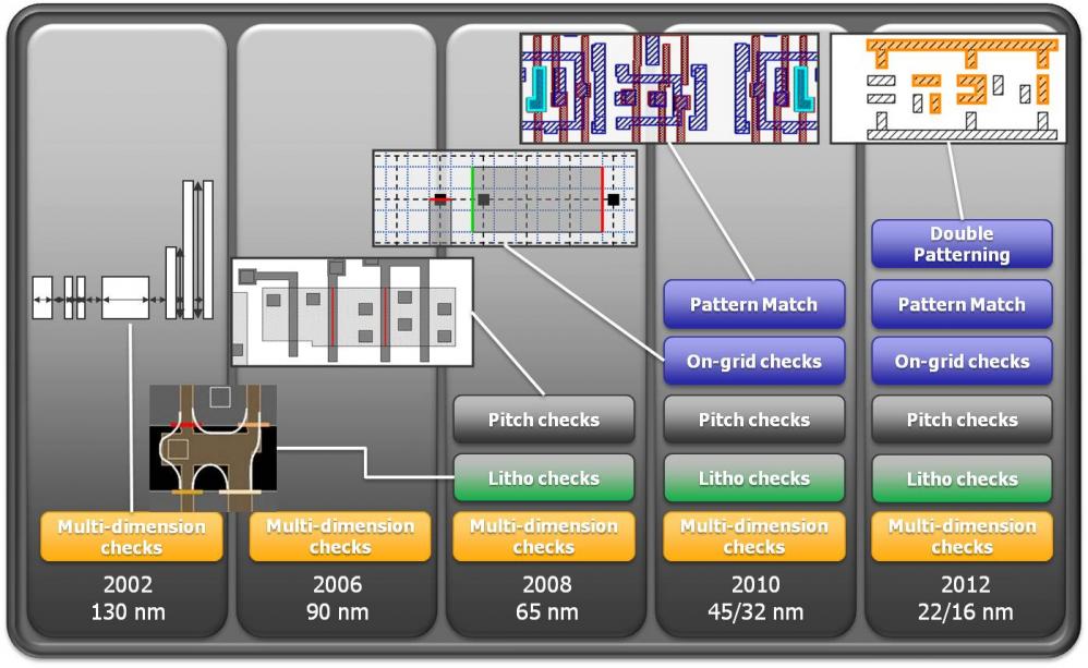
With each process generation, the design rules get more and more complex. One datapoint: there are twice as many checks at 28nm as there are at 90nm. In fact, the complexity of the rules is outpacing the ability to describe them using the simplified approaches used in the DRCs built-into layout editors or formats like LEF.

Worse still, at 28nm and below the rules are really too complicated for a designer to understand. As Richard Rouse of MoSys said “at 28nm, even the metal rules are incomprehensible.” It goes without saying that the rules for the even more critical layers for transistor formation are even more opaque.

It is going to get worse too, since at 22nm and below we will need to use double patterning for the most critical layers, which means that it is not really even possible to know whether a design is in compliance, that depends on the double patterning algorithm being able to assign shapes to the two patterns in a way that the lithography will work.

It used to be that analog designers were comfortable staying a couple of nodes behind the digital guys but that is no longer possible. 70% of designs are mixed-signal SoCs, driven by the communications market in particular. Mobile consumer chips need analog, and even some of the digital, such as graphics accelerators, typically require custom design datapaths.

Digital designs are about scaling, using simplified rules to be able to handle enormous designs. Custom and analog design is about optimization and so need to push to the limits of what the process can deliver.

The only solution to this problem is to run the real signoff DRC with the real signoff rules. The signoff DRC is pretty much universally Mentor’s Calibre (sorry Cadence and Synopsys). But running Calibre from within theLaker™ Custom Layout Automation System is inconveniently slow and disruptive. So Mentor have created an integratable version called Calibre RealTime (and by the way, doesn’t Mentor know that Oasys have a product already called RealTime Designer) which operates on top of the OpenAccess (OA) database and Laker is the first, and so far only, layout editor to do the integration. Rules are continuously checked in parallel with editing. A full check takes about 0.2 to 0.3 seconds. In the demonstration I saw at Springsoft’s booth it was almost instantaneous, rather like the spell-checker in a word processor. In fact at 28nm it was checking 6649 shapes in 0.3 second. Laker optimizes which checks are required based on what changes were made to the design (if you don’t change the metal you don’t need to run those metal checks again, for example) which further improves performance.

Historically, layout designers have been very reluctant to adopt anything that might slow them down. But the complexity of the rules in modern process nodes along with the high performance and unobtrusiveness of the integration, has a good chance of immediate adoption of the Laker signoff-driven layout flow.


Moore’s Law and Semiconductor Design and Manufacturing

Moore’s Law and Semiconductor Design and Manufacturing
by Daniel Nenni on 03-12-2011 at 4:51 am

The semiconductor design and manufacturing challenges at 40nm and 28nm are a direct result ofMoore’s Law, the climbing transistor count and shrinking geometries. It’s a process AND design issue and the interaction is at the transistor level. Transistors may be shrinking, but atoms aren’t. So now it actually matters when even a few atoms are out of place. So process variations, whether they are statistical, proximity, or otherwise, have got to be thoughtfully accounted for, if we are to achieve low-power, high-performance, and high yield design goals.

"The primary problem today, as we take 40 nm into production, is variability,” he says. “There is only so much the process engineers can do to reduce process-based variations in critical quantities. We can characterize the variations, and, in fact, we have very good models today. But they are time-consuming models to use. So, most of our customers still don’t use statistical-design techniques. That means, unavoidably, that we must leave some performance on the table.”Dr. Jack Sun, TSMC Vice President of R&D

Transistor level design which lnclude Mixed Signal, Analog/RF, Embedded Memory, Standard Cell, and I/O, are the most susceptible to parametric yield issues caused by process variation.

Process variation may occur for many reasons during manufacturing, such as minor changes in humidity or tempature changes in the clean-room when wafers are transported, or due to non uniformities introduced during process steps resulting in variation in gate oxide, doping, and lithography; bottom line it changes the performance of the transistors.

The most commonly used technique for estimating the effects of process variation is to run SPICE simulations using digital process corners provided by the foundry as part of the spice models in the process design kit (PDK). This concept is universally familiar to transistor level designers, and digital corners are generally run for most analog designs as part of the design process.

Digital process corners are provided by the foundry and are typically determined by Idsat characterization data for N and P channel transistors. Plus and minus three sigma points maybe selected to represent Fast and Slow corners for these devices. These corners are provided to represent process variation that the designer must account for in their designs. This variation can cause significant changes in the duty cycle and slew rate of digital signals, and can sometimes result in catastrophic failure of the entire system.
However, digital corners have three important characteristics that limit their use as accurate indicators of variation bounds especially for analog designs:

  • Digital corners account for global variation, are developed for a digital design context and are represented as “slow” and “fast” which is irrelevant in analog design.
  • Digital corners do not include local variation effects which is critical in analog design.
  • Digital corners are not design-specific which is necessary to determine the impact of variation on varying analog circuit and topology types.

These characteristics limit the accuracy of the digital corners, and analog designers are left with considerable guesswork or heuristics as to the true effects of variation on their designs. The industry standard workaround for this limitation has been to include ample design margins (over-design) to compensate for the unknown effects of process variation. However, this comes at a cost of larger than necessary design area, as well as higher than necessary power consumption, which increases manufacturing costs and makes products less competitive. The other option is to guess at how much to tighten design margins, which can put design yield at risk (under-design). In some cases under and over-design can co-exist for different output parameters for a circuit as shown below. The figure shows simulation results for digital corners as well as Monte Carlo simulations which are representative of the actual variation distribution.

To estimate device mismatch effects and other local process variation effects, the designer may apply a suite of ad-hoc design methods which typically only very broadly estimate whether mismatch is likely to be a problem or not. These methods often require modification of the schematic and are imprecise estimators. For example, a designer may add a voltage source for one device in a current mirror to simulate the effects of a voltage offset.

The most reliable and commonly used method for measuring the effects of process variation is Monte Carlo analysis, which simulates a set of random statistical samples based on statistical process models. Since SPICE simulations take time to run (seconds to hours) and the number of design variables is typically high (1000s or more), it is commonly the case that the sample size is too small to make reliable statistical conclusions about design yield. Rather, Monte Carlo analysis is used as a statistical test to suggest that it is likely that the design will not result in catastrophic yield loss. Monte Carlo analysis typically takes hours to days to run, which prohibits its use in a fast, iterative statistical design flow, where the designer tunes the design, then verifies with Monte Carlo analysis, and repeats. For this reason, it is common practice to over-margin in anticipation of local process variation effects rather than to carefully tune the design to consider the actual process variation effects. Monte Carlo is therefore best suited as a rough verification tool that is typically run once at the end of the design cycle.

The solution is a fast, iterative AMS Reference Flow that captures all relevant variation effects into a design-specific corner based flow which represents process variation (global and local) as well as environmental variation (temperature and voltage).

Graphical data provided by Solido Design Automation‘s Variation Designer.