You are currently viewing SemiWiki as a guest which gives you limited access to the site. To view blog comments and experience other SemiWiki features you must be a registered member. Registration is fast, simple, and absolutely free so please, join our community today!
Dan is joined by Dr. Jason Cong, the Volgenau Chair for Engineering Excellence Professor at the UCLA Computer Science Department. He is the director of the Center for Domain-Specific Computing and the director of VLSI Architecture, Synthesis, and Technology Laboratory. Dr. Cong’s research interests include novel architectures and compilation for customizable computing, synthesis of VLSI circuits and systems, and quantum computing.
Dr. Cong will be recognized by the Electronic System Design Alliance and the Council on Electronic Design Automation (CEDA) of the IEEE with the 2024 Phil Kaufman Award at a presentation and banquet on November 6 in San Jose, California.
In this far-reaching discussion, Dan explores the many contributions Jason has made to the semiconductor industry. His advanced research in FPGA design automation from from the circuit to system levels is discussed, along with the many successful companies he has catalyzed as a serial entrepreneur.
Dr. Cong is also inspiring a future generation of innovators through his teaching and research in areas such as quantum computing. He explores methods to inspire his students and the path to democratizing chip design, making it readily available to a wide range of new innovations.
The views, thoughts, and opinions expressed in these podcasts belong solely to the speaker, and not to the speaker’s employer, organization, committee or any other group or individual.
Douglas Smith has focused his career on optimizing advanced technologies for high volume ASIC applications. He has led elite design teams at Motorola SPS then Broadcom for over 25 years. With 200+ successful tape outs generating $10B+ in revenue. Douglas left Broadcom to self-fund a startup focused on advanced memory technologies. He has assembled an elite design and business team to provide differentiated memory solutions to his customers.
Tell us about your company
Veevx is a fabless semiconductor company created by a veteran team of engineering architects that left Broadcom’s central engineering group to form a company focused on technology innovations to build products for the market needs. We were founded 2.5 years ago in Mesa, AZ with 20 people split between the US and India.
What problems are you solving?
Our products bring cloud level AI performance to mobile and edge devices. Processing typically performed in the cloud can be done directly on a mobile or edge devices allowing end users to do translations, AI assistance, VR & AR functions locally. This provides low latency, user tailored experience, privacy with longer battery life & higher security, giving better user experience.
We also provide technology to overcome the memory wall. AI functionally is driving the demand for high performance local memory (SRAM). The manufacturing processes and limitations imposed by device physics restricts SRAM scaling as CMOS nodes shrink. This increases memory costs.
Customers want advances in memory technology to overcome the limitations of SRAM. We will soon sample our iRAM to customers. iRAM is an advanced memory chiplet that is packaged with our customers’ microcontroller. It gives their devices more memory, in the same footprint, at significant power savings.
How do you enable your customers?
We are focused on mobile and low power edge devices. Our product enables end customers to perform rich AI functions, typically done in the data center, on the devices. This eliminates the latency of going to the data center, enhances privacy because the data stays on device and in some cases, reduces cost and power.
How do you differentiate from others in this arena?
Veevx specializes in new memory technology and mixed signal compute. Many academic and R&D papers discuss the advantages of compute in memory and how mixed signal compute is required to reduce the processing power while also increasing the performance for AI accelerators. Our team has decades of experience productizing new technology into silicon and specializes in the area needed for an ultra-low power AI accelerator compute product.
What new features/technology are you working on?
High-performance/Ultra-low power compute by integrating mixed signal compute directly into the memory architecture. We take ultra-low power MRAM and add innovations to increase the performance of the memory cells while adding innovative mixed signal compute to our silicon verified ultra-low power MRAM to maximize the compute in memory performance and energy efficiency. Our solution mitigates the power and latency by avoiding data movement to the processor. Our mixed signal compute is flexible to perform the mathematical operations used in AI using 1/100 the power of traditional digital compute engines. We want to keep our accelerator flexible so as models continue to evolve, we will be able to run the operations on our accelerator.
Can you tell us about your experience of being a Silicon Catalyst incubator company?
Being a Silicon Catalyst portfolio company for the past year and a half has been an invaluable experience for us. The incubator has accelerated our development by providing essential tools and foundry access through their in-kind partnerships resources that are often out of reach for startups.
They have offered us a platform to showcase our products and innovations to a wide industry audience, which has been instrumental in increasing our visibility and credibility in the market.
Moreover, Silicon Catalyst’s extensive network of experienced advisors, relevant investors, and collaborative customers has opened doors to new opportunities and partnerships. This support system has not only enhanced our technological capabilities but also propelled our business growth.
How do customers normally engage with your company?
We are a fabless semiconductor company that sells chips in chiplet (bare die) or in packaged form.
Customers can engage with Veevx via direct inquiries on our website, at industry conferences, and through our business development team.
We also engage in research and development collaboration projects with customer engineering teams to customize our products to their specific needs.
Electronics production in the major developed countries has been showing slow growth or declines in 2024. United States electronics production three-month-average change versus a year ago (3/12 change) was 0.4% in July 2024, the slowest since the pandemic year of 2020. Growth has been slowing since averaging 6.5% in 2022 and 2.3% in 2023. Japan has gone from averaging 6.0% 3/12 growth in 2023 to a 2% decline in June 2024. The 27 countries of the European Union (EU27) have reported declining electronics production since May 2023, except for a 3.2% increase in May 2024. In June 2024, EU27 production was down 8.0%. United Kingdom (UK) production has been declining since September 2023, except for a 0.7% increase in February 2024. UK production was down 3.7% in July 2024.
In contrast, most developing Asian countries are experiencing strong growth in electronics production. Taiwan and South Korea are considered developed countries, but their electronics industries are still emerging. Beginning in mid-2023, these countries showed a turnaround in production.
Taiwan has been the strongest country in Asia, with 3/12 production (measured in New Taiwan dollars) moving from a 3.2% decline in June 2023 to an increase of 49% in July 2024. This growth has been driven by computers, with production in January through July 2024 doubled versus January-July 2023. Much of the computer boom can be attributed to AI servers. Market Research firm MIC estimates Taiwan produces 90% of global AI servers. TrendForce projects the US dollar value of the AI server market will grow 69% in 2024.
Vietnam has also shown a strong turnaround in electronics production. The low in 3/12 change was negative 10.8% in May 2023. 3/12 growth was over 20% in June and July 2024. Vietnam has benefited from Samsung’s $22 billion investment in the country. Vietnam produces about half of Samsung’s smartphones.
South Korea’s production turnaround was more recent, with 3/12 production change negative in February through April 2024. Production turned positive in May 2024 at 3.2% and reached 23.8% growth in July 2024. Labor strikes this year at Samsung likely had an impact on production trends. The strong September growth may be a temporary blip.
India is demonstrating healthy electronics production growth, with July 2024 3/12 growth of 14%. 3/12 change had been negative from October 2022 through March 2024. India has benefited from multinational companies increasing manufacturing in the country. Apple has begun manufacturing its latest generation of iPhones, the 16 series, in India. Apple plans to produce 25% of its iPhones in India by 2025, up from about 14% last year, shifting production from China. Lenovo announced this month it has started making AI servers in India for local consumption and export. The government of India projects the country will double its electronics manufacturing over the next five years.
China remains the dominant electronics manufacturer in Asia, but growth has slowed as companies shift manufacturing to other countries. China’s 3/12 production change turned positive in April 2023 and peaked at 13.8% in June 2024. August 2024 3/12 growth was 12.3%, slower than the July data for the other countries in the chart.
The trend of weak electronics production growth in the U.S, Europe and Japan will likely continue for at least the next few years. Asia will remain the growth driver. Political and economic pressures affecting China will lead to continuing production shifts to other Asian nations. India seems poised for strong growth due to its huge labor force, low labor rates, and significant investment by multinational electronics companies.
Semiconductor Intelligence is a consulting firm providing market analysis, market insights and company analysis for anyone involved in the semiconductor industry – manufacturers, designers, foundries, suppliers, users or investors. Please contact me if you would like further information.
Bill Jewell
Semiconductor Intelligence, LLC
billjewell@sc-iq.com
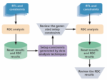
The complexity of System-on-Chip (SoC) designs continues to rise at an accelerated rate, with design complexity doubling approximately every two years. This increasing complexity makes verification a more difficult and time-consuming task for design engineers. Among the key verification challenges is managing reset domain crossing (RDC) issues, particularly in designs that utilize multiple asynchronous resets. RDC occurs when data is transferred between different reset domains.
While the use of Electronrc Design Automation (EDA) tools for clock domain crossing (CDC) verification has become a common practice, the verification of RDCs—an equally important aspect—has only recently gained prominence. RDC verification is necessary to ensure data stability between asynchronous reset domains. Failure to do so can hide timing and metastability issues in a SoC, resulting in unpredictable behavior during its operation.
RDC verification tools are essential for detecting potential metastability issues in designs, but they generate vast amounts of data—often millions of RDC paths. Engineers must manually analyze this data to find common root causes for violations and apply appropriate constraints. This process is both time-consuming and error-prone, often leading to multiple design iterations that delay project timelines.
One of the primary challenges is the sheer volume of RDC violations reported, especially in the early stages of design when no constraints have been applied. The lack of proper constraints related to reset ordering, reset grouping, and isolation signals can lead to false violations and unnecessary debugging effort. Design teams can spend weeks analyzing these violations manually, often overlooking critical issues or spending too much time on trivial paths.
Addressing RDC Challenges with Data Analytics
The manual approach to RDC verification is no longer sufficient given the complexity of modern SoC designs. Advanced data analytics and supervised data processing techniques offer a promising solution. These techniques can quickly analyze the vast amounts of data generated by RDC tools, identify patterns, and suggest optimal setup constraints. By recognizing common root causes of violations, such as incorrect reset domain grouping or reset ordering issues, data analytics techniques provide recommendations for constraints that can be applied to resolve multiple RDC paths at once. These constraints may include stable signal declarations, reset ordering specifications, reset domains, isolation signals, and constant declarations.
Figure 1. RDC verification using data analysis techniques.
Key Recommendations for Improving RDC Verification
Several specific recommendations are identified in the whitepaper, to reduce RDC violations through automated data analysis.
Reset Ordering: Ensuring that the receiver flop’s reset is asserted before the transmitter flop’s reset can prevent metastability. If proper ordering constraints are not defined, RDC tools may flag multiple violations due to this common issue. For example, if reset RST2 (receiver) is asserted before RST1 (transmitter), it ensures that metastability does not propagate downstream.
Synchronous Reset Domains: RDC issues arise when reset signals for the source and destination registers are asynchronous. Grouping resets into synchronous reset domains during setup reduces the number of reported crossings.
Directive Specifications: Defining valid constraints for specific design scenarios can prevent unnecessary RDC violations. For example, if a receiving register’s clock is off when a transmitter register’s reset is asserted, there is no risk of metastability, and the tool should not report a violation. Neglecting such constraints leads to noisy results.
Stable Signals: Some signals within the design may not contribute to metastability despite being part of asynchronous reset domains. If these are not marked as stable, they will be incorrectly flagged as potential violations.
Isolation Signals: Isolation techniques can prevent metastability by isolating data transfer between reset domains during asynchronous reset assertion. Properly specified isolation constraints reduce the number of RDC paths requiring manual review.
Non-Resettable Receiver Registers: In some cases, non-resettable registers (NRR) may not pose a metastability risk if a downstream register in the same reset domain exists. Failing to specify such conditions leads to false violations.
Case Study: Data Analytics in Action
A case study was conducted to evaluate the effectiveness of using data analytics in RDC verification. The design in question consisted of 263,657 register bits, multiple clock domains, and nine reset domains. Initial RDC verification runs with manually applied constraints identified approximately 8,000 RDC paths.
After applying advanced data analytics techniques, a consolidated report was generated, recommending several constraints. These constraints addressed reset ordering, data isolation, and synchronous reset domain grouping, among other issues. Following the application of these recommendations, the number of RDC violations dropped from 8,000 to 2,732—a more than 60% reduction in violations.
The use of a threshold value of 200 (indicating constraints would be recommended only if they impacted at least 200 paths) helped streamline the process, focusing on high-impact issues and minimizing noise. The time to reach RDC verification closure was reduced from ten days to under four days, showcasing the significant time savings from data-driven analysis.
Results and Impact
The case study demonstrated that the application of data analytics to RDC verification can lead to a significant reduction in unsynchronized crossings and violations. By systematically identifying root causes and applying targeted constraints, verification engineers were able to resolve up to 60% of RDC violations without manual intervention. This reduction in violations accelerated the verification closure process and improved overall design quality. Additionally, the flexibility provided by the analytics approach—allowing engineers to focus on high-impact suggestions—streamlined the debugging process and ensured that effort was invested in solving critical design issues.
The table below shows the results from applying data analytics techniques to RDC verification of five different designs.
Summary
As SoC designs grow in complexity, traditional manual RDC verification methods are not scalable. By incorporating advanced data analytics into the verification process, engineers can significantly reduce closure time, improve result quality, and avoid costly silicon respins. These techniques not only accelerate root cause identification but also provide actionable insights through constraint recommendations that target common design issues. This automated approach ensures that real design bugs are addressed early, reducing metastability risks and strengthening the final SoC design. Integrating these methods into existing verification flows promises to save time and effort while delivering higher-quality, error-free designs.
Even though this is the 16th OIP event please remember that TSMC has been working closely with EDA and IP companies for 20+ years with reference flows and other design enablement and silicon verification activities. The father of OIP officially is Dr. Morris Chang who named it the Grand Alliance. However, Dr. Cliff Hou is the one who actually created the OIP which is now the largest and strongest ecosystem in the history of semiconductors.
I spent a good portion of my career working with EDA and IP companies on foundry partnerships as well as foundries as a customer strategist. In fact, I still do and it is one of the most rewarding experiences of my career. Hsinchu was my second home for many years and the hospitality of the Taiwan people is unmatched. That same hospitality is a big part of the TSMC culture and part of the reason why they are the most trusted technology and capacity provider.
Bottom line: If anyone thinks this 20+ years of customer centric collaboration can be replicated or reproduced, it cannot, the OIP is a moving target, it expands and gets stronger every year. An ecosystem is also driven by the success of the company and in no part of history has TSMC been MORE successful than today, my opinion.
We will be covering the event in more detail next week but I wanted to share my first thoughts starting with a quote from a blog published yesterday by Dan Kochpatcharin, Head of Ecosystem and Alliance Management Division at TSMC. I met Dan 20 years ago when he was at Chartered Semiconductor. For the last 17 years he has been at TSMC where he started as Deputy Director of the TSMC IP Alliance (working for Cliff Hou) which is now a big part of the TSMC OIP.
“Our collaboration with TSMC on advanced silicon solutions for our AWS-designed Nitro, Graviton, Trainium, and Inferentia chips enables us to push the boundaries of advanced process and packaging technologies, providing our customers with the best price performance for virtually any workload running on AWS.” – Gary Szilagyi, vice president, Annapurna Labs at AWS
Readers of the SemiWiki Forum will get this inside joke and if you think this quote from AWS is a coincidence you are wrong. C.C. Wei has a very competitive sense of humor!
Dr. L.C. Lu (Vice President of Research & Development / Design & Technology Platform) did the keynote which was quite good. I first met L.C. when he was in charge of the internal TSMC IP group working for Cliff Hou. He is a very smart no nonsense guy who is also a great leader. Coincidentally, L.C. and CC Wei both have P.h.D.s from Yale.
Some of the slides were very similar to the earlier TSMC Symposium slides which tells you that TSMC means what it says and says what it means. There were no schedule changes, it was all about implementation, implementation, and implementation.
L.C. did an interesting update on Design-Technology Co-Optimization (DTCO). I first heard of DTCO in 2022 and it really is the combination of design and process optimization. I do know customers who are using it but this is the first time I have seen actual silicon results. Remember, this is two years in the making for N3 FinFlex.
The numbers L.C. shared were impressive. In order to do real DTCO a foundry has to have both strong customer and EDA support and TSMC has the strongest. For energy efficiency (power savings) N3 customers are seeing 8%-20% power reductions and 6%-38% improvement in logic density depending on the fin configuration.
L.C. also shared DTCO numbers for N2 NanoFlex and the coming A16 SPR (Super Power Rail) which were all in the double digits (11%-30%). I do know quite a few customers who are designing to N2, in fact, it is just about all of TSMC’s N3 customers I am told. It will be interesting to see more customer numbers next year.
L.C. talked about packaging as well which we will cover in another blog but let me tell you this: By the end of 2024 CoWos will have more than 150 tape-outs from more than 25 different companies! And last I heard TSMC CoWos capacity will more than quadruple from 2023 levels by the end of 2026. Packaging is one of the reasons why I feel that the semiconductor industry has never been more exciting than it is today, absolutely!
Part 2 of this 4-part series reviews the role of virtual prototypes as stand-alone tools and their use in hybrid emulation for early software validation, a practice known as the “shift-left” methodology. It assesses the differences among these approaches, focusing on their pros and cons.
Virtual Prototyping and Hybrid Emulation for Early Software Validation
Debugging a software stack for complex System-on-Chip (SoC) designs is a highly iterative process, often requiring the execution of trillions of verification cycles even before end-user applications are considered. For instance, booting Android can take anywhere from 20 seconds to one minute at 1 GHz, depending on the version and end-application, which equates to at least 20 billion cycles. Rebooting this mobile OS ten times a day consumes at least 200 billion cycles. When end-user workloads are factored in, the challenge intensifies, adding more trillions of cycles.
Given the immensity of this task, an effective methodology is essential to support software development teams. Various electronic design automation (EDA) tools and methods are available to address the challenges in response to the exponentially growing demand for processing cycles as one progresses up the software stack.
Hardware Description Language (HDL) Simulators: Viable for Bare-metal Software Validation
At the bottom of the stack, traditional hardware description language (HDL) simulators can be used for bare-metal software validation. However, HDL simulators do not scale with the increasing complexity of hardware designs and the related software complexity. For example, simulating a 100 million gate-equivalent design may advance at a rate of one cycle per second or slower, approximately six orders of magnitude lower than the throughput achievable with hardware-assisted verification engines. This significantly restricts their deployment to block-level or small IP designs, already during the early stages of the verification cycle.
Virtual-based and Hardware-assisted Platforms: Necessary for Early SW Bring-up on SoCs
To meet the demanding requirements of software validation on SoC designs, two primary approaches are prevalent:
Virtual Prototypes: Extensively used for early software development, testing and validation when Register Transfer Level (RTL) code is still under development
Hardware-Assisted Verification (HAV) Platforms: Valuable when the RTL is completed, or at least when the necessary hardware blocks and subsystems for software development are available.
Virtual prototypes and HAV platforms possess the processing power to execute billions of verification cycles within feasible timeframes, enabling multiple iterations per hour–or, for very large designs, per day.
Each of these approaches serves different objectives at different stages of the design verification process, providing a balanced solution to the growing challenges in hardware and software development.
Virtual Prototyping: Effective Methodology for Early Software Validation
A virtual prototype is a fully functional software model, typically described in C/C++, that represents an electronic system under development. It can model anything from a single SoC to a multi-die system or an entire electronic system, such as a network of electronic control units (ECUs) in a vehicle. Unlike an RTL model of equivalent functionality, a virtual prototype is considerably slimmer and operates at much higher speeds, often approaching real-world performance. It includes a fast processor model (instruction-set simulator) along with memory and register-accurate peripheral models, all integrated into a binary-compatible representation of the entire system.
Virtual prototypes are ideal platforms for validating the entire, unmodified software stack from bare-metal software to firmware, device drivers, operating systems, middleware, and applications. Their key advantage lies in their early availability during the design cycle, preceding RTL finalization. This early availability enables software engineers to start development in parallel with, or even ahead of, hardware development.
In addition, virtual prototypes can be shared with not only the internal development team but also with technology partners and key customers early in the design process. This collaborative approach allows iterative feedback, enabling external stakeholders to contribute to fine tuning the final product.
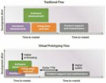
Ultimately, virtual prototypes enable software validation before RTL is available, streamline the development process, and accelerate tape out, resulting in reduced design costs. (See figure 1.)
Figure 1. Virtual Prototypes accelerate time-to-market with higher quality and fewer resources. Source: Synopsys
Virtual Prototyping Commercial Offerings
Today, several electronic design automation (EDA) companies offer virtual prototyping solutions that include libraries of components to address a broad range of design possibilities. The comprehensive nature of these libraries significantly decreases adoption costs for end users, as the modeling effort required for their specific virtual prototypes is substantially lower when most virtual models are readily available off-the-shelf. These solutions also feature robust support for design visualization and software debugging tools, enhancing the users’ ability to develop, analyze, debug, and optimize the software stacks driving their SoC designs effectively.
IP companies play a crucial role in the virtual prototyping ecosystem by supplying models of their IP. For early software validation, models of processor IPs and peripheral IPs are the most relevant.
Some of the leading providers of virtual prototypes include:
Arm
Arm offers a comprehensive catalog of Arm Fast Models (AFM), covering a wide range of processors and system IP. This comprises models for all Cortex processors, Neoverse processors, and various system IP components such as interconnects, memory management units, and peripherals.
RISC-V Virtual Models from IP providers
RISC-V instruction set simulators (ISS) for virtual platforms are available for various RISC-V variants, provided by research institutions and commercial processor IP vendors such as Synopsys, SiFive, Andes or OpenHW. These processor models are primarily based on two technologies, Imperas[1] Fast Processor Models (ImperasFPM) and QEMU (Quick Emulator).
Synopsys RISC-V Models
Synopsys offers the most comprehensive model library of IP Model Library, which includes Synopsys Interface IP, ARC processor IP and leading third-party embedded processor IP. Among them are Imperas Fast Processor Models (ImperasFPM) that cover the complete range of RISC-V standard extensions as well as vendor-specific extensions. Other processors models embrace those from Andes, Codasip, Imagination, Intel, lowRISC, Microsemi, MIPS, NSI-TEXE, OpenHW Group, SiFive, and Tenstorrent. In addition to their use in virtual platforms, these models are used in tools for design verification, as well as for analyzing and profiling RISC-V processors.
Quick Emulator (QEMU)
QEMU is an open-source framework used to create virtual prototypes of complete SoCs, comprising processors and their peripheral models. Open-source initiatives, such as those from Lenovo, are releasing processor models in QEMU for selected processors, such as the Arm Cortex-A series. Additionally, other processor companies are supporting the open-source ecosystem by enabling the creation of QEMU models for their RISC-V cores.
Virtualizer Development Kits (VDKs)
One of the critical barriers to deploying virtual prototypes is the rapid assembly and packaging for easy distribution. The Synopsys Virtualizer tool suite addresses this challenge by providing a large library of IP models, streamlining the creation of virtual prototypes. Teams can further extend and customize these prototypes with their own peripheral models, guided by the tool.
These prototypes can then be packaged as Virtualizer Development Kits (VDKs), which include a suite of efficient debug and analysis tools, as well as sample software. Notably, VDKs integrate seamlessly with leading embedded software debuggers, enabling software bring-up without requiring changes to existing development workflows. VDKs can represent systems ranging from a processor core and SoC to hardware boards and electronic systems, such as a network of electronic control units (ECUs) in a vehicle.
Additionally, Synopsys offers design services to help users fully leverage the capabilities of their VDKs, ensuring they maximize the potential of their virtual prototypes.
Hybrid Emulation: Bridging the Gap for Software Bring-up and Hardware Verification
The hierarchical design process of a SoC begins with a high-level description that assists the design team with multiple tasks. In the initial phase, the high-level description captures the design specifications and intent, enabling early validation of these tasks. Concurrently, it supports early software development through virtual prototyping.
As the design creation process progresses, the high-level description is decomposed into sub-systems and individual blocks, with details added through RTL descriptions. At this stage, co-simulating high-level description of design code and RTL code hinders the speed of execution of virtual prototypes because of the increased complexity of the RTL.
The solution comes through Hybrid Emulation, which leverages the strengths of both virtual prototyping and hardware emulation, creating a powerful synergy that enhances the design verification process.
Virtual Prototyping excels at high-speed execution, allowing unmodified production software to run on a virtualized version of the target hardware, enabling early software bring-up.
Hardware Emulation achieves cycle-accurate and fast execution of the RTL blocks and sub-systems, providing a detailed and accurate environment for hardware verification.
While both techniques offer significant speed advantages when deployed in their intended targets, integrating them presents challenges at the interface level where communication between virtual prototypes and hardware emulation occurs. This interface can often become a bottleneck, reducing the overall performance of the hybrid system.
To overcome this, the industry has established the Accellera’s SCE-MI (Standard Co-Emulation Modeling Interface) standard. This standard defines efficient protocols for data exchange between the virtual prototype and the emulated hardware, ensuring reliable, high-speed communication necessary to optimize the hybrid emulation process.
Hybrid Emulation Enables the Shift-Left Verification Methodology
Hybrid emulation enables the concurrent verification of hardware and validation of software by harnessing the fast performance of virtual machines with the accuracy of hardware emulation. The approach speeds up the entire verification and validation process, often referred to as “shift-left” methodology for moving it upstream on the process timeline. Yet, it comes with caveats.
In this hybrid environment, two separate runtime domains arise, each tailored to one of the two tools.
High-Performance Virtual Prototype: This domain can reach performance of hundreds of million instructions per second (MIPS). The fast environment allows tasks like booting a Linux OS in just a few minutes, compared to over an hour in traditional emulation.
Cycle-Accurate RTL Emulation: The RTL emulation domain performs at a speed of a few megahertz equating to few MIPS. Although slower, the emulator provides cycle-accurate hardware verification.
The performance disparity between the virtual machine environment and the RTL section can offer speed advantages, particularly for software-bound systems where software execution dictates overall performance. In such cases, the virtual machine can advance rapidly, significantly boosting the speed of software development and testing. Conversely, in hardware-bound systems, where the performance of the RTL code is the limiting factor, the overall speed improvement is minimal. Given that many software development tasks are software-bound, hybrid emulation proves to be highly beneficial for supporting software teams. See figure 2.
Figure 2. Acceleration of software bring-up and hardware-assisted verification via Hybrid Emulation (Shift-left Methodology). Source: Synopsys
Conclusions
Virtual prototyping and hybrid emulation are essential tools for efficient and effective development and debug of the software stack in modern SoC designs. When combined, they form a strategy that embodies the concept of ‘Shift Left’, a shift away from the traditional sequential hardware and software development.
By supporting a unified workflow, the “Shift-Left” methodology encourages close collaboration between hardware and software teams, enabling them to work in parallel, share critical insights, and complement each other’s efforts. This convergence speeds up the verification cycle, uncovers integration issues early on, enhances efficiency, and significantly expedites the time-to-market for SOC development.
How do you measure safety for a DNN? There is no obvious way to screen for a subset of safety-critical nodes in the systolic array at the heart of DNNs. Paul Cunningham (GM, Verification at Cadence), Raúl Camposano (Silicon Catalyst, entrepreneur, former Synopsys CTO and now Silvaco CTO) and I continue our series on research ideas. As always, feedback welcome.
Think FMEDA has safety compliance locked down? Not so in AI accelerators, where what constitutes a safety-critical error in the hardware cannot be decoupled from the model running on the hardware. Research here is quite new but already it is clear that the rulebook for faulting, measurement, and ultimately safety mitigation must be re-thought for this class of hardware.
There are multiple recent papers in this field, some of which we may review in later blogs. This paper is a start, taking one view of what errors mean in this context (misclassification) and what tests should be run (a subset of representative test images). On the second point, the authors provide important suggestions on how to trim the test set to a level amenable to repeated re-analysis in realistic design schedules.
Paul’s view
Intriguing paper this month: how do you check that an autonomous drive AI accelerator in a car is free of hardware faults? This can be done at manufacturing time with scan chains and test patterns, but what about faults occurring later during the lifetime of the car? One way is to have duplicate AI hardware (known in the industry as “dual lock step”) and continuously compare outputs to check they are the same. But of course this literally doubles the cost, and AI accelerators are not cheap. They also consume a lot of power so dual lockstep drains the battery faster. Another is built-in-self-test (BIST) logic, which can be run each time the car is turned on. This is a good practical solution.
This paper proposes using a special set of test images that are carefully selected to be edge cases for the AI hardware to correctly classify. These test images can be run at power on and checked for correct classification, giving a BIST-like confidence but without needing the overhead of BIST logic. Unfortunately, the authors don’t give any direct comparisons between their method and commercial BIST approaches, but they do clearly explain their method and credibly argue that with only a very small number of test images, it is possible to detect almost all stuck-at faults in a 256×256 MAC AI accelerator.
The authors propose two methods to pick the edge case images. The second method is by far the best and is also easy to explain: the final layer of a neural network used to classify images has one neuron for each object type being classified (e.g. person, car, road sign, …). Each of these neurons outputs a numerical confidence score (0 to 1) that the image contains that object. The neuron with the highest confidence score wins. The authors sort all the training images by the max confidence score of all their neuron outputs and then use the n images with the lowest max confidence scores as their edge case BIST images. They present results on 3 different open-source image classification benchmarks. Injecting faults into the AI accelerator that cause it to have a 5% mis-classification rate, using 10 randomly selected images for BIST achieves only 25% fault coverage. Using their edge-case selection method to pick 10 images gives 100% fault coverage. Intuitive and effective result.
Raúl’s view
In March, we blogged about SiFI-AI, which simulated transient faults in DNN accelerators using fast AI inference and cycle-accurate RTL simulation. The results showed a “low” error probability of 2-8%, confirming the resilience of DNNs, but not acceptable for Functional Safety (FuSa) in many applications. This month’s paper explores both transient and permanent faults in DNN accelerators to assess FuSa, aiming to create a small set of test vectors that cover all FuSa violations.
The used configuration consists of 1) a Deep Neural Network (DNN) featuring three fully connected hidden layers with architecture 784-256-256-256-10, 2) a systolic array accelerator similar to Google’s Tensor Processing Unit (TPU) that has a 256 x 256 Multiply-Accumulate (MAC) array of 24-bit units, and 3) three datasets for image classification with 60,000 training and 10,000 test images: MNIST, a benchmark of digit images, F-MNIST a set of 10 fashion images, and CIFAR-10 a set of images in 10 classes.
The paper performs a FuSa assessment on inference of the fully trained DNN running on the systolic array, injecting various faults into the systolic array reused for all DNN layers. The error-free DNN shows a classification accuracy of 97.4%. Obvious and not so obvious findings include:
Errors in less significant bit positions have lower impact, in the accumulator from the 9th bit onwards no effect.
Accumulator errors drop accuracy by about 80%, while multiplier errors cause only a 10% drop.
More injected faults lead to greater accuracy reductions.
Activation functions affect accuracy: ReLU results in about an 80% drop, whereas Sigmoid and Tanh result in around a 40% drop.
Data sets also impact accuracy: MNIST and F-MNIST have about an 80% drop, while CIFAR-10 has only a 30% drop.
The key section of the paper focuses on how to select test cases for detecting FuSa violations (any reduction in accuracy). The primary insight is that instead of using random nondeterministic patterns from the entire input space, which mostly do not correspond to an image and cannot be classified by a DNN, the proposed algorithms choose specific patterns from the pool of test vectors in the application data set for FuSa violation detection. The first algorithm calculates the Euclidean distance of each test case from multiple classes in the data set and selects those that resemble multiple classes. The outcomes are remarkable: with only 14-109 test cases, 100% FuSA coverage is achieved. Another algorithm picks the k patterns that have the lowest prediction confidence values, where the number k of test patterns is set by the user. With just k=10 test patterns, which is 0.1% of the total 10,000, all FuSA violations are identified. The authors also present results for a larger DNN with 5 hidden layers and a bigger data set containing 112,800 training and 18,800 test images, achieving similar outcomes.
This is an enjoyable paper to read. The title “Towards Functional Safety” hints at not ready for practical application, due to the limited dataset of merely 10,000 images and just 10 classes. It remains open whether this approach would be effective in scenarios with significantly larger datasets and categories, such as automotive applications, face recognition, or weapon detection.
It is a well-known fact that chiplets provide several advantages over traditional monolithic chips. Despite these benefits, the transition to a chiplet-based design paradigm presents challenges that need coordinated efforts across the industry. In essence, collaborative efforts among various players involved are not just a nicety, but rather a hard requirement to realize the full benefits. And an ASIC provider can optimize the benefits even further by customizing the various chiplet components of a design.
I recently interviewed Erez Shaizaf, the CTO of Alchip Technologies, Limited, to gain deeper insights into how the combination of the chiplet-paradigm and an ASIC approach can maximize the benefits to be derived from chiplets. Alchip is a leading provider of silicon design and production services for merchant silicon and system companies developing complex and high-volume ASICs and SoCs. Here are the excerpts from that interview.
The Importance of Collaboration in Chiplet-Based Design
In a fast-paced industry where new tape-outs occur every 12 to 18 months, having the right technology is only part of the solution. Efficient execution is equally critical. Chiplet-based designs and advanced packaging technologies are inherently complex, requiring a multi-disciplinary approach to achieve peak performance and maximize financial returns. Extensive collaboration across the ASIC value chain ensures seamless integration from the architecture phase to design, all the way to mass production ramp-up.
Alchip’s Collaborative Efforts
Alchip collaborates closely with IP vendors, EDA providers, foundries, and assembly partners to ensure seamless integration of cutting-edge technologies into advanced packaging designs. This includes managing high-bandwidth memory and numerous UCIe lanes for high die-to-die bandwidth, along with 224G/PCIe multi-lane architectures to support both scale-up and scale-out needs. By partnering with EDA vendors across all stages of design, from RTL to GDS, and through package design and sign-off phases, Alchip streamlines design processes, optimizing them for rapid production and reduced time to market.
In addition to its work with EDA vendors, Alchip collaborates with foundries such as TSMC to ensure compatibility with advanced process nodes and packaging types. This holistic approach extends to assembly and testing partners to validate designs and accelerate the transition from tape-out to mass production. Through optimized package and interposer multi-die floor planning and careful supply chain management, Alchip enables high-volume production efficiently, meeting diverse customer needs while minimizing risk and ensuring smooth transitions from design to mass production within the shortest possible time.
Critical Role of ASIC Providers in the Chiplet Ecosystem
Despite the buzz surrounding chiplets, Alchip challenges the notion of a “chiplet market.” In reality, chiplet development remains largely captive, with an estimated 90% of chiplet development occurring internally within organizations (with the exception of high-bandwidth memory). Each customer has unique performance demands — spanning functionality, bandwidth, process node, and package type — that make a generalized chiplet market hard to foresee.
However, Alchip has taken proactive steps to address these challenges by developing the Soft Chiplet approach, a modular, front-end ready design that allows for rapid tape-out. This modular approach covers various aspects of chiplet design — including verification, firmware, delivery, documentation, and ready-to-harden flow. The Soft Chiplet is an embodiment of Alchip’s collaborative philosophy, allowing flexibility for different customer requirements while speeding up the tape-out process.
Handling Design Complexity in Multi-Die Systems
Designing multi-die systems and chiplet-based architectures introduce significant complexity. Alchip navigates this challenge by leveraging its talented engineering team, who continuously seek out the best new solutions. The Alchip team drives the ecosystem to innovate and collaborate in meeting customer demands.
Additionally, Alchip’s R&D efforts ensure that the company is always prepared for “the next node” — whether it’s 5nm, 3nm, or beyond. This approach positions the company to provide customers with the most cutting-edge technologies when they need them, ensuring faster tape-outs and more efficient designs.
Packaging Solutions for Chiplet Integration
Alchip supports all TSMC advanced packaging types, as well as certain advanced OSAT packaging solutions, to ensure optimal compatibility with diverse chiplet integration needs. These packaging solutions are critical for achieving the best possible performance and power efficiency in chiplet-based designs. Through its internal R&D efforts, Alchip continuously develops packaging solutions that address the evolving demands of its customers, ensuring high performance and efficient integration across a wide range of applications.
Success Stories
Alchip is a trusted partner for cloud service providers, merchant silicon companies, and innovative start-ups, each of whom has unique design and performance requirements. The company’s ability to tailor ASIC solutions to these varying needs underlines its value as a collaborative partner. However, due to the custom nature of these designs, specific case studies remain confidential.
Summary
Alchip is dedicated to pushing the boundaries of the chiplet ecosystem through collaboration and continuous technological progress. It is actively advancing its Soft Chiplet initiative, with a working prototype expected by the end of this year. This development is part of a broader roadmap aimed at building a flexible and collaborative ecosystem for chiplet-based systems. The company plans to reveal more about its advancements in chiplet technology at upcoming conferences.
By: Dr. Charlie Su, President and CTO, Andes Technology Corp.
At Andes Technology, we are excited to share some of our latest advancements and insights into the growing role of RISC-V in several high-performance applications. According to the SHD Group report, “IP Market RISC-V Market Report: Application Forecasts in a Heterogeneous World,” our processor IPs account for 30% of RISC-V shipments, making Andes the number one competitor in the market. This gives us unique visibility into the deployment of the RISC-V ISA worldwide. Our customers offer products for a diverse range of applications across AI/ML, automotive, communication/networking, microcontroller, mobile, and storage sectors.
Leading Innovations in AI Acceleration
AI has been one of our largest licensing markets for our vector processors and advanced CPUs, targeting applications ranging from low-power edge devices—such as smart home devices, wearable health monitors, predictive maintenance in industrial settings, and autonomous drones and robots—to the high-performance cloud AI and data centers, with customers like Meta and Sapeon.
Meta announced their first Meta Training Inference Accelerator (MTIA) at ISCA 2023. It featured an 8×8 64 PE (processing element) array. Each PE includes a processor subsystem incorporating two configurations of the Andes AX25-V100, the predecessor of Andes popular NX27V vector processor. Meta also leveraged Andes Custom Extensions (ACE) and COPILOT tools to heavily customize the cores to their unique requirements, significantly reducing their design teams’ engineering time.
Meta noted in their ISCA presentation: “Each PE contains two RISC-V cores… and are heavily customized to suit the functionalities needed… The set of customizations includes custom interfaces, custom registers, custom instructions, and custom exceptions… The focus and strategy when architecting the accelerator therefore has been on adopting and reusing suitable pieces of technology, as well as tools and environments, from vendors and the open-source community….”
Our NX27V and AX45MPV vector processors, and other advanced Andes cores, are key components in next-generation in-memory computing solutions. Customers such as Axelera, Houmo.AI, Rain AI, and TetraMem leverage our technology for their in-memory computing AI accelerators. Most recently, our customer Rivos commented that our NX45 in their high-end AI SoC is the only RISC-V core passing their rigorous verification tests.
A pioneer in compute-in-memory (CIM) technology, Rain AI licensed Andes’ AX45MPV RISC-V vector processor. The AX45MPV CPU future-proofs Rain’s CIM-based NPU by allowing the addition of custom instructions to encapsulate the CIM computing blocks, thereby greatly simplifying software development efforts, esp. for the AI compiler. Andes Custom Extension framework and its automated COPILOT tool streamlines this customization process as highlighted in the Rain AI’s talk in the recent Andes RISC-V CON.
AI continues to be an area of rapid innovation, making it a perfect fit for RISC-V. For example, Lightelligence is developing photonics-based AI accelerators performing high-speed matrix multiplication—another exciting area where our vector processors play a crucial role.
Automotive and ADAS (Advanced Driver Assistance Systems) are also growth markets. Our automotive customers use our Vector and Safety-Enabled family of RISC-V cores across a variety of applications including in-cabin monitoring, display, radar, and sensing/control. Multiple customers have utilized our fully ISO26262-compliant products and safety packages, achieving product safety certification in record time!
Additionally, our traditional markets such as processors for media-rich computing platforms (e.g, smartphones, tablets, and TVs), signal processing in wireless communications, and general-purpose control, remain strong. For example, Renesas uses Andes AX45MP for their Linux-capable MPU, the RZ/Five. The significant growth in high-performance AI and Automotive combined with the rapidly expanding software ecosystem is also driving growth in the high-performance general-purpose processing segment.
New and repeat customers continue to value the flexibility, openness, and rapid time-to-market that is enabled by Andes commercial RISC-V IP coupled with our COPILOT toolset for custom extensions. We are seeing this growth persist in our traditional markets of embedded control, DSP, and real-time systems. More importantly, this growth is accelerating in AI, Automotive, and General Compute.
Enhanced Software Ecosystem and Innovations
The RISC-V software ecosystem for control processors is rapidly expanding, with support from GNU, LLVM, Linux, and Google’s official support for Android. Linux already has robust RISC-V support, from the toolchain to booting into various Linux distributions. The RISC-V Software Ecosystem (RISE) Project, formed by Andes and other key RISC-V companies, is actively working to enhance open-source support for application processors, recently bringing up support for Java 21 and 22.
Andes is heavily involved in RISE, currently contributing to compilers for supporting ever-increasing memory space and to QEMU (Quick EMUlator) for adding new RISC-V extensions such as IOPMP, which is a powerful fast simulation framework to enable early software exploration and development while SoC architecture is still on the drawing board.
Under the RISE project, Andes is also responsible to portimize (port & optimize) the entire OP-TEE (Open Portable Trusted Execution Environment), a trusted application framework, to RISC-V. With OP-TEE, RISC-V will have a competitive offering to ARM’s TrustZone software. OP-TEE provides the software level protection, while ePMP (Enhanced Physical Memory Protection) and IOPMP (Input/Output Physical Memory Protection) hardware level protection. These advanced memory protection features enhance system security and reliability by providing fine-grained control over permissions of memory accesses from RISC-V processors and other DMA-capable controllers, crucial for high-security applications. The porting of OP-TEE calls for significant work in TEE Client API and OP-TEE Linux Driver in the Non-secure World as well as TEE core API and OP-TEE OS in the Secure World. Underlying the Secure and Non-secure World is the OpenSBI layer, which Andes will enhance with OP-TEE extensions. OpenSBI (Open Supervisor Binary Interface) is another critical component in the RISC-V ecosystem, providing the necessary firmware layer to boot and manage RISC-V operating systems and hypervisors.
Regarding Android, Google has specified the base requirements for RISC-V in the Compatibility Definition Document (CDD). This includes RVA22 plus vector, vector crypto, and hypervisor support. Andes has been working on the ongoing Android Open-Source Project (AOSP) software by bringing them to run on QEMU and porting it to our non-compatible hardware to achieve faster performance for Android. During this process, we even identified some generic bugs present in ARM builds, which Google acknowledged and fixed.
We also focused on optimizing computational libraries using RISC-V Vector extension (RVV), such as libjpeg—the widely used library for handling JPEG images, offering efficient compression, decompression, and manipulation capabilities, and working on optimization for ART (Android Runtime). The Android Runtime (ART) represents a significant evolution in the Android platform’s runtime environment, offering substantial improvements in performance, efficiency, and developer productivity over its predecessor, Dalvik. By leveraging AOT (Ahead-of-Time) and JIT (Just-In-Time) compilation, enhanced garbage collection, and better debugging tools, ART provides a more responsive and efficient runtime for Android applications.
Conclusion
Andes Technology continues to deliver advanced RISC-V processor IP while making extensive contributions to its software ecosystem. Our collaborations with industry leaders in the AI, automotive, and computing sectors highlight the versatility and potential of RISC-V architecture. Through our robust hardware solutions and the ever-enriched RISC-V software ecosystem, we are paving the way for RISC-V to become a mainstream choice for high-performance computing applications. With ongoing efforts in compiler enhancements, runtime and library optimizations, trusted application framework, and support for critical industry standards, Andes Technology is leading the way in realizing the full potential of RISC-V. We are excited about the future possibilities and innovations, solidifying our position in the evolving landscape of high-performance computing.
As the demand for higher performance computing solutions grows, so does the need for faster, more efficient data communication between components in complex multi-die system-on-chip (SoC) designs. In response to these needs, Synopsys has introduced the world’s fastest UCIe-based IP solution, capable of operating at a groundbreaking 40Gbps. This full IP solution, encompassing Controller, PHY, and Verification IP, represents a leap forward for die-to-die connectivity in SoCs, targeting data centers, AI, generative AI, and a wide array of cutting-edge applications.
What sets this solution apart is that it achieves 40Gbps per pin, a 25% increase over the 32Gbps defined in the UCIe specification, without compromising energy efficiency or die area. This capability opens up new possibilities for end users while maintaining seamless integration with the UCIe ecosystem.
During a chat with Michael Posner, vice president of IP product management at Synopsys, he commented that their active contribution to the UCIe consortium is what enabled the company to deliver a robust UCIe solution soon after the UCIe 2.0 ratification. Delivering robust IP solutions ahead of a standard’s ratification has become routine for Synopsys as noticed with Ethernet 1.6T and PCIe 7.0 IP solution announcements.
The UCIe Advantage: An Industry Standard for Die-to-Die Connectivity
Universal Chiplet Interconnect Express (UCIe) has emerged as the de facto standard for die-to-die connectivity, offering a scalable solution for high-performance, multi-die designs. The key metrics of UCIe — bandwidth per mm², power efficiency, low latency, and minimal area usage — align perfectly with the needs of customers across various industries, from data centers to AI applications.
Why 40Gbps?
Synopsys’ new IP solution is UCIe compliant at 32Gbps per pin and goes beyond it, offering speeds up to 40Gbps per pin in specific use cases. By increasing the data transfer rate to 40Gbps, the company ensures that multi-die SoCs can efficiently handle the growing data requirements in these environments. While pushing the boundaries beyond the UCIe specification, the solution is able to provide more bandwidth without impacting the energy or area budgets of the design. This is particularly leverageable and beneficial in environments where dies are tightly linked, such as in multi-die architectures that need to efficiently transfer massive amounts of data between SoC components. The additional bandwidth provided by the 40Gbps solution allows system designers to future-proof their designs while meeting current demands.
Modular Architecture for Scalable Bandwidth
A significant advantage of this UCIe IP solution is its modular architecture. The PHY component of the IP consists of 64 Tx and 64 Rx lanes, which can be combined to create large-scale solutions with substantial bandwidth. This makes the solution ideal for memory-intensive applications, such as those using high-bandwidth memory (HBM) chiplets. In these designs, high-speed die-to-die communication is essential to ensure the performance of memory subsystems. The Synopsys UCIe solution’s 40Gbps capability offers an extra margin of performance for these applications, ensuring that memory bandwidth requirements are not only met but exceeded, allowing for greater flexibility in SoC design. This flexibility allows designers to optimize for both area and performance, achieving high data throughput without sacrificing valuable chip real estate.
“Heterogeneous integration with high-bandwidth die-to-die connectivity gives us the opportunity to deliver new memory chiplets with the efficiency needed for data-intensive AI applications,” said Jongwoo Lee, vice president of the System LSI IP Development Team at Samsung Electronics. “Leveraging Synopsys’ new 40G UCIe IP, we can extend our collaboration to develop industry-leading chiplet solutions for tomorrow’s high-performance data centers.”
With Synopsys’ solutions like PCIe 7.0 and Ethernet 1.6T already addressing the need for high-bandwidth data coming into SoCs, UCIe provides the means for that data to flow between dies seamlessly.
Signal Integrity Monitors: Enabling Reliable Mission-Critical Operations
The UCIe IP solution includes Signal Integrity Monitors which monitor the integrity of the links for identifying any degradation in performance. When any degradation is noticed, the system can be flagged for taking any proactive maintenance measures or the profiled information can be offloaded for further analysis.
The ability to assess link degradation and flag for corrective action before a failure occurs ensures higher reliability and reduces the risk of downtime. Synopsys 40G UCIe IP offers silicon lifecycle management (SLM) features, where data from the profiling process can be used for longer-term reliability assessments. A proactive approach to reliability is especially important for industries like data centers and automotive, where continuous operation and safety are paramount. Further, this feature is expected to be a game-changer in industries like automotive, where real-time data integrity is also essential for reliable vehicle operations.
UCIe’s Redundant Links and Lifecycle Management
The UCIe specification defines redundant links to enhance reliability. Synopsys’ UCIe solution supports redundant links and links found to be defective can be rerouted to spare links during manufacturing or testing.
Simplified Clocking for Easy Integration
The company has further reduced system integration complexity by incorporating built-in clocking capabilities that make use of a 100MHz reference clock, a standard across SoC designs for many years. UCIe typically requires a 1GHz or 2GHz clock, but by integrating the capability to work with a more common 100MHz clock, the company has simplified system-level integration, allowing designers to adopt the technology more easily without the need for complex clocking inputs.
Hardware-Based Initialization: A Key Differentiator
Another unique aspect of the company’s UCIe-based IP is its hardware-based initialization, which eliminates the need for processor or firmware interaction during the bring-up process. The company has simplified this process by developing a system that allows the UCIe link to come online without external intervention, greatly reducing the complexity and cost associated with multi-die designs.
This capability is particularly important in “blind die bring-up” scenarios, where the only connection between two dies is the UCIe link. By eliminating the need for firmware or processor involvement in establishing the link, the company reduces the need for complex software solutions, saving time and reducing development costs.
Summary
With its new UCIe IP solution, capable of operating at 40Gbps per pin, Synopsys has advanced die-to-die communication technology for high-performance AI SoCs. By delivering 25% more bandwidth than the UCIe specification without impacting energy or area, the company is enabling designers to meet the needs of today’s data-intensive applications, while ensuring scalability for future generations.
The modular architecture, integrated Signal Integrity Monitors and test features, protocol bridges and simplified clocking provide a robust, scalable solution for high-bandwidth, low-latency SoC designs. As industries continue to shift towards multi-die architectures, the company’s 40Gbps UCIe IP offers a powerful tool for system designers looking to optimize performance, reliability, and ease of integration.