Human nature never ceases to amaze me. I understand the recent economic turmoil and looming National Debt has thrown us for a loop but please, let us all get some perspective here and in the words of Rodney King, “Can we all get along?”
A clever little scumbag recently registered the domain danielnenni.com and is now hawking event tickets in my name. I let the domain expire after moving my blogging to SemiWiki. Shame on me for being too cheap to protect my legal name. Daniel Nenni is not a trademark so this is a case of identity theft. Life is short so I will probably just let it go but still, not a good sign of the human condition.
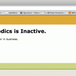
Even worse is the dispute between Methodics and IC Manage. A discussion on SemiWiki started on June 30[SUP]th[/SUP] with the screen shot above. You can visit the thread HEREbut let me summarize. Apparently someone, who chose to hide their identity, registered the domain www.methodics.comand put up the message that the web page is no longer active, the company is no longer in business, and listed IC Manage as an alternative source. IC Manage and Methodics DA compete in the design data management business. The official Methodics response is HERE.
As a grand finale, last week I got this email from Mike Sottak. Mike is a long time EDA PR guy who I have worked with in the past. Mike has always proved to be a solid guy so I have no problem posting his email. I must also mention that SemiWiki works with another competitor to IC Manage and Methodics which is ClioSoft.
You may be aware of the recent shenanigans perpetrated against the design data management company Methodics. It seems the domain name www.methodics.com (which Methodics does not currently own) was set up to point visitors to the web site of their competitor IC Manage. The blatant attempt to confuse customers went so far at one point as to suggest Methodics was no longer in business. While there was little doubt that IC Manage was behind this, it wasn’t until Methodics initiated something called a Uniform Domain Name Dispute Resolution complaint with the World Intellectual Property Organization that the smoking gun was revealed. WIPO confirmed the previously-hidden registrant/owner of the domain is indeed the Vice President of ICManage.
Full disclosure: Methodics is a client of mine. But this incident strikes a personal chord with me as someone who has worked in the EDA industry for more than 20 years. They did not ask that I write to you on their behalf. I do so because I have not seen a more offensive act of malicious and unethical tactics in my career (and many of you will recall that I was at Cadence during the infamous Avanti trade secret theft case). We as an industry often get criticized for being immature and self-defeating. It’s not hard to understand why customers and other people on the periphery of EDA would think that given this type of behavior. The fact that Shiv Shikand has the arrogance to register the domain name that rightly belongs to his main competitor IN HIS OWN NAME sets a new standard for disregard of business ethics.
So why should you care? I believe that part of the role of any press or media outlet is to help police the areas they cover by holding people, companies and other institutions accountable for their actions. I therefore urge you as a key influencer of our industry to call IC Manage to the carpet on this one. I am certain that if a similar situation occurred between Synopsys, Mentor or Cadence, you would do the appropriate reporting and analysis.
I can assure you that Methodics is not interested in this purely as PR stunt, and in fact would prefer that the whole issue go away and the domain name be rightfully transferred to them. But they have been violated in no uncertain terms and have been unfairly been taken advantage of by an unscrupulous competitor. If you are in any way involved with EDA, I believe this type of behavior must be exposed for what it is. Or do we continue to look the other way and condone it through our silence, perpetuating the image of an industry that is immature and risky with which to do business?
Kind regards
Mike Sottak
Wired Island PR
Below is the report from WIPO:
<methodics.com>
Notice of Change in Registrant Information
Dear Complainant,
Further to our Acknowledgment of Receipt of Complaint, please be advised of
the following:
The registrant of the disputed domain name in the above referenced
proceeding has been identified by the concerned Registrar, Blue Razor
Domains, as being different to the entity named in the Complaint as
Respondent. The registrant information we have received from the Registrar
is as follows:
Registrant:
Shiv Sikand
15729 Los Gatos Blvd
Suite 100
Los Gatos, CA 95032
United States
Administrative Contact:
Sikand, Shiv shiv@icmanage.com
15729 Los Gatos Blvd
Suite 100
Los Gatos, CA 95032
United States
+1.4083588191
Technical Contact:
Sikand, Shiv shiv@icmanage.com
15729 Los Gatos Blvd
Suite 100
Los Gatos, CA 95032
United States
+1.4083588191
Setting the legalities of this situation aside, If this story is true, morally and ethically this is just WRONG!I have seen a lot of dirty deeds in my 25+ years in EDA but this absolutely takes the prize! Please voice your opinion in the comment section and I will make sure they get to IC Manage. If you have disputing data please send it to me and I will include it in this post.
Again, I’m biased. I had coffee with Shiv Sikand to try and smooth things over after he attacked SemiWiki on a LinkedIn group when we started working with his competitor ClioSoft. We ended up yelling at each other in a Peet’s Coffee, Shiv and his company IC Manage are still banned from SemiWiki.
*** Shiv had posted a response HERE but it has since been taken down. It was probably one of the worst apologies I have seen.