RVN! 26 Banner revised (800 x 100 px) (600 x 100 px)

#49 Design Automation Conference Deadlines

#49 Design Automation Conference Deadlines
by Paul McLellan on 01-14-2012 at 10:53 pm

Note that there are several DAC deadlines coming up in the next couple of weeks.

The deadline for user track submissions is January 17th (next Tuesday). Submission requires an extended abstract. See here for details.

The deadline for DAC workshops is January 19th (next Thursday). A proposal is required. See here for details.

The deadline for the P.O. Pistilli Scholarship is February 1st. There is an application form to be filled in. See here for details.

As always, the DAC website is at dac.com and the DAC blog is at blog.dac.com where, if you don’t get your fill of my writing here, you can get even more of it.


Thanks to Linkedin members: 24 “Like” given to “Interface Protocols, USB3, HDMI, MIPI… the winner and losers in 2011”

Thanks to Linkedin members: 24 “Like” given to “Interface Protocols, USB3, HDMI, MIPI… the winner and losers in 2011”
by Eric Esteve on 01-14-2012 at 12:53 pm

Just because it seems that the likes given to: Interface Protocols, USB3, HDMI, MIPI… the winner and losers in 2011 were numerous, I decided to count it.

Twenty-four likes received, in 11 Linkedin groups (see below), that’s good! Very goos! Thanks to all of you… And most probably thanks to IPNESTfor the quality of the data.

If you did not read this post, it maybe the right time to do it! You will find many, many useful information about USB 3.0, HDMI, DisplayPort, MIPI and more


Eric Esteve
from IPNEST

And now the list:

Semiconductor Wiki Project (www.SemiWiki.com )

Pascal Lo Ré, Jan Willis like this

Semiconductor – VLSI

Cheng Kuan Yin, Kanak Rajput and 1 other like this

Processor/SoC/Systems Architecture, RTL Design Professionals

BAHLOUL Skander likes this

Texas Instruments

Chen Song Chaw Chen Song likes this

Microelectronics Network

Stephane Cordova, Mike Engbretson and 1 other like this

China Semiconductor Professional Network 中国集成电路专业人士协会

Steve Cheng likes this

High Speed Interface Design Professionals

Suto Hiroyuki, Michael Baker and 2 others like this

ANALOG MIXED SIGNAL

Roland MOBEANG, Kevin Ho like this

Semiconductor – Sales & Marketing

Chuck Dube likes this

Chuck Dube • Any thoughts on wireless HDMI (or whatever it’s called). Basically, the 60Ghz or so wireless interface between displays and video equipment. It seems 802.11ac? may be a contender.

Franz Dugand • The soon to be released 802.11ac may be the leading technology for wireless video streaming in the coming years. It has new features tailored for video streaming, and is using 5GHz band, so less crowded than 2.4GHz, and less expensive/challenging than 60GHz. Backward compatible with 802.11n, 802.11ac will probably be very popular in TV, STB and DVD players, those equipment being more and more connected to the internet.

MIPI Alliance

Michael Herz, Thierry Campiche and 3 others like this

VERIFICATION IP – VIP
Mehul Kumar likes this


The Innovator’s Dilemma Dagger Aimed at AMD and nVidia’s Heart

The Innovator’s Dilemma Dagger Aimed at AMD and nVidia’s Heart
by Ed McKernan on 01-13-2012 at 1:42 pm

There is one semiconductor company that for the last 3 years has outperformed ARM and more than doubled in stock price relative to Apple. They are everywhere but barely known to most. The success of this company in the coming year though could result in the leveling of AMD and nVidia as they try to adjust to the economics of the mobile Tsunami, which means the commoditization of application processors. The company is Imagination Technologies, whose graphics IP is in many mobile processors including Apple’s ARM family and Intel’s latest Atom processors.

Clayton Christensen described in his book the Innovators Dilemma the difficulty and reluctance that companies have of going into new markets that effectively cannibalize existing high margin businesses. One of the examples that Christensen focuses on is the disk drive industry in which every few years a new leader would emerge to displace the previous leader who was focused on maximizing its market share and profits instead of forging ahead with an eventual replacement. One of the key drivers of the replacement was a smaller form factor device (higher density was always understood to be a requirement).

What happens however, to Christensen’s model when in the midst of a massive increase in graphics capability there is a clash with an even greater force called personal mobility (or ultra mobility). The shift from desktop to notebook happened over many years and was considerably more gradual than what we have seen in just the last 4 years when the Internet was placed in the palm of one’s hand with the Smartphone. The first order of business for Apple, Samsung, HTC and others has been to shoehorn all the electronics in an area that has no tolerance for excessive heat. Something had to give.

Open any souped-up desktop PC with the latest AMD or nVidia graphics card and you realize that the cooling infrastructure has overshot that of the processor and indeed it is a supercomputer. The massive R&D budgets employed by AMD and nVidia are intended to win the gamers and then over a couple of Moore’s Law generations trickle down to the notebook, tablet and then Smartphone.

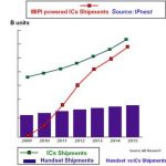
In typical, Innovator’s Dilemma fashion, Imagination Technologies has come from the ground up to challenge AMD and nVidia’s from the rear in an area that both are trying to catch up. This will be difficult for both to do because of the head start that Imagination Technologies has had in licensing its technology to Apple, Intel, Qualcomm, TI and Samsung. Indeed ARM feels threatened. Against this array of competitors, nVidia sits alone. The company has seen revenue more than double over the past three years and operating profit margins exceed that of AMD and nVidia by a wide margin. You could say that the Innovator’s Dilemma formula has been extended to take into account how an IP business model is superior to a Fabless Business Model.

Intel’s push in the very slim ultrabook form factor is already reducing nVidia and AMD’s share in the PC space. With Imagination Technologies licensing its graphics technology to the Fab players (Intel, Samsung and yes Apple – I consider them virtual fab) there is a squeeze on nVidia and AMD from above and below. All of this was driven by a major form factor shrinkage in PCs and Smartphones that was unforeseen just a few years ago but is dramatically reshaping the industry.

For AMD to survive, I believe they have to become an IP design House for Google, Samsung, Qualcomm, Amazon, HTC or other major player. Pure Fabless, with no shared investment, is no longer a model that survives up against the Fab Titans: Intel and Samsung. Companies must move to one side or the other: IP House or Fab Focused. If I can make a play of words on Jerry Sanders famous quote: Real Men Have Fabs or Real Men Live in IP Houses.

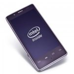
I find it interesting that in all of this transformation, Intel has decided that it needs Imagination Technologies for its low end Atom. Another sign that Paul Otellini believes Intel’s future value is really based on process technology and not chip architectures. Intel has never been able to keep up with nVidia on graphics but it way outperforms TSMC in process development. Imagination Technologies is able to give nVidia a run for its money in the graphics space and as a result have outperformed them financially. As a comparison over the past three years, nVidia’s revenue has been flat and is down since 2007 – perhaps a sign that the cliff is near.

FULL DISCLOSURE: I am Long AAPL, INTC, QCOM, ALTR


Needham growth conference

Needham growth conference
by Paul McLellan on 01-13-2012 at 6:00 am

One of the fun things when a company gets big but is still private, like Atrenta, is that you start to get invited to events like the Needham Growth Conference that took place earlier this week in New York. When I ran Compass Design Automation, which at the time was about $55M in revenue, I remember going to a couple of these events. At one level this seems like a pointless exercise since nobody can buy the stock. But there are actually two reasons that analysts should be interested. Firstly, when a company gets big enough, it can have an effect on the results of the other companies in the industry that are public. And secondly, when the company is big enough it starts to be plausible that it might have an IPO in the future, and an analyst who has a good understanding of the industry should not be hearing about it for the first time on the roadshow.

So this week, Bert Clement, the CFO of Atrenta was at the Needham conference for his 15 minutes of fame (plus 5 more for questions). Of course the audience is primarily financial types so the focus is not so much on Atrenta’s technology. Just getting the audience to understand that you are in EDA and which part you serve is enough of a challenge.

So what did Bert say. Firstly, that Atrenta is focused on SoC realization where it is really the only company today, and SpyGlass is pretty much the standard. They have 170 customers including 19 of the top 20 semiconductor companies. They have had eight consecutive years of revenue growth, are profitable and growing. They should do about $45M this year and margins are growing over time. So they are one of the largest and healthiest private EDA companies. They have over 300 employees with over 200 in R&D.

SoC Realization actually occupies an interesting niche in the spectrum of EDA areas. Below SoC realization is classic EDA, tools to build the actual SoC. This has single digit growth and is experiencing consolidation of suppliers (Synopsys/Magma being the most significant). Above SoC Realization is system design. It has double digit growth but the market is very fragmented and has a low TAM as a result. In the middle, SoC Reallization has double digit growth, an expanding supplier base of IP and IP companies, and is fuelled by the need for consumer products that incorporate a lot of IP to build very complex SoCs (think smartphones and tablets).


EDAC reports Q3

EDAC reports Q3
by Paul McLellan on 01-12-2012 at 7:49 pm

EDAC (EDA consortium) market statistics service announced the data for Q3 of 2011. Revenue increased 18.1% (versus 2010) to $1543.9 million. Sequentially (versus Q2) revenue increase 7.4%. Annualized, that puts EDA at over $6B for, I belive, the first time ever. Wally Rhines, who is EDAC chair (and CEO of Mentor) commented that “growth was exceptionally robust across the board, in every product category and every region.”

Breaking it down:

  • CAE revenue was $566.7 million (10.5% up on Q3 2010)
  • IC physical design and verification was $338.3 million (16% up on 2010)
  • PCB and MCM was $140.3 million (up 11.6% on 2010)
  • Semiconductor intellectual property, or what we usually just call IP, was $510 million (up a huge 37.4% from last year)
  • Services was $88.7 million (up 13.1% on 2010)

By region the numbers were all up too:

  • North America purchased $706.7M of products and services (up 22.4% on 2010)
  • Europe, Middle East and Africa (EMEA) was $257.9 million (up 14.9% on 2010)
  • Japan was $256.9 million (up 11.1% on 2010)
  • APAC was $322.4 million (up 17.6% on 2010)

Historically Q4 is the biggest quarter, with year-end budgets available and salespeople’s quota plans going into overdrive. Cadence is first to report since their financial year ended at the end of the calendar year. Synopsys, Mentor and Magma are all offset.


The EDAC Market Statistics Service page is here.


Advanced Memory Cell Characterization with Calibre xACT 3D

Advanced Memory Cell Characterization with Calibre xACT 3D
by SStalnaker on 01-12-2012 at 7:18 pm

Advanced process technologies for manufacturing computer chips enable more functionality, higher performance, and low power through smaller sizes. Memory bits on a chip are predicted to double every two years to keep up with the demand for increased performance.

To meet these new requirements for performance and power, memory designers must increase bit density while satisfying exacting specifications for fast data transfer and low power consumption. Unfortunately, higher density increases the interactions among interconnects and devices, making it harder to ensure that memories will meet all specifications and be manufacturable with high yield. Ultimately, this means that more accurate characterization than ever before is required at every step of memory design.

Traditional extraction methods used for memory designs have proven unable to address these challenges, either because they are too slow, or are not accurate enough, or both. Memory designers need tools that can help them analyze parasitic issues accurately and quickly at every stage of the physical design cycle, from basic building blocks to the full chip.

A fast field solver, such as Calibre xACT 3D, can be used to apply boundary conditions on a bit cell (Figure 1). By specifying a closed boundary for the cell, the designer can improve parasitic extraction and simulation accuracy, as well as performance for a symmetric design. Using boundary conditions, bit cell geometries are effectively modeled as a reflected or periodic repeated pattern on all sides of the boundary, at the same distance. This allows the designer to extract a single bit cell accurately without having to construct an array.

Figure 1: Application of boundary conditions on a cell

This modeling technique enables designers to radically speed up their characterization process and realize a design that performs to their specification. For example, using Calibre xACT 3D, we extracted a bit cell in 4 seconds, whereas a popular reference-level field solver required 2.15 hours. The total capacitance of the nets extracted from the bit cell compared very closely to the reference results.

Using fast field solver technology like Calibre xACT 3D at all stages of memory design, from bit cell design to full chip sign-off, ensures a robust design that will work to specification when it is manufactured.

To read the complete white paper, click here.

Leave a comment or contact Claudia Relyea if you would like to discuss how Calibre xACT 3D can help your company ensure the successful and timely development of high-performance, low-power memory designs at advanced nodes.


Memory Controller IP, battle field where Cadence and Synopsys are really fighting face to face. Today let’s have a look at Cadence’s strategy.

Memory Controller IP, battle field where Cadence and Synopsys are really fighting face to face. Today let’s have a look at Cadence’s strategy.
by Eric Esteve on 01-12-2012 at 9:45 am

I have shared with you last year some strategic information released by Cadence in April about their IP strategy, more specifically about the launch of the DDR4 Controller IP. And try to understand Cadence strategy about Interface IP in general (USB, PCIe, SATA, DDRn, HDMI, MIPI…) and how Cadence is positioned in respect with their closest and more successful competitor in this field, Synopsys.
Continue reading “Memory Controller IP, battle field where Cadence and Synopsys are really fighting face to face. Today let’s have a look at Cadence’s strategy.”


Speeding SoC timing closure

Speeding SoC timing closure
by Paul McLellan on 01-12-2012 at 1:42 am

As chips have become larger, one of the more challenging steps is full-chip signoff. Lots of other steps in the design process can work on just a part of the problem, but by definition full-chip signoff has to work on the full chip. But it is not just that chips have got larger, the number of corners that need to be validated has also exploded. And, of course, signoff is the last step before tapeout and so is on a critical part of the critical path under the most intense schedule pressure.

Over the last year or so Magma has introduced a suite of tools to address these issues. The first tool is the QCP extractor. You can’t have accurate timing without accurate parasitic data. The next tool is Tekton for delay calculation and static timing analysis. And thirdly there is Quartz DRC/LVS for physical verification.

These tools are multi-threaded and so scale to very large designs and can take advantage of compute farms. A further optimization is multi-mode, multi-corner analysis and extraction that allow a single server to concurrently analyze many scenarios and thus reduce the time and resources required. Magma’s place and route is now also built on top of these same basic extraction and analysis engines, thus removing correlation problems that can arise if the place and route system uses an approximation that the subsequent verification flags as incorrect.

There is a new webinar that explains how the sign-off technologies enhance the overall flow and are integrated together into a complete sign-off solution.


Medfield: ARM twisting

Medfield: ARM twisting
by Paul McLellan on 01-11-2012 at 2:53 pm

One of the most significant announcements at the consumer electronics show (CES) this week was Intel’s Medfield, an Atom-based smartphone SoC. The SoC itself is unremarkable, perhaps a little better than ARM Cortex-based SoCs in some areas, worse in others. The reason it is significant is that Motorola (soon to be Google, don’t forget) announced a multi-year partnership with the first products expected this summer, and Lenovo actually demoed a smartphone containing the chip.

I used to think that Intel had very little chance in the mobile marketplace because ARM was so entrenched and there just wasn’t any good reason to switch. Plus Intel’s big weakness is that they are hopeless at software. They previously tried to get into the communications business with an Xscale (ARM) strategy but gave up after investing over a billion dollars without really getting any customers. Last year they bought Infineon’s wireless business (also ARM-based) but they promptly lost their flagship customer, Apple, to Qualcomm. They have had an unsuccessful Atom-based phone SoC, Moorestown, that went nowhere.

But Android has leveled the playing field so Intel doesn’t need to be good at software development. There is little lock-in of Android to ARM-based systems and as more and more of the software is further and further from the hardware, the details of the hardware matter less and less for the software developer. With a little care, an Android-based app should run on any Android phone without really even knowing what the processor is (Android apps are (mostly) written in Java and so are actually compiled into Java Virtual Machine bytecodes not the underlying assembly in any case).

The important aspect of the announcement is not that Intel is going to seriously impact ARM-based phones in the short term. It is not. It is simply that Intel is seriously in the game. And once it is seriously in the game it will be able to leverage its lead in process technology which will soon put it about 2 process generations ahead of TSMC (or anyone else for that matter). Even if there are some inherent weaknesses in the Atom architecture versus ARM Cortex, two processes generations is simply too big a chasm to get across and a TSMC/ARM SoC will be inferior to an Intel/Atom SoC.

I wouldn’t be the least bit surprised if Intel hasn’t been making some trips across the valley to a famous Cupertino-based smartphone company.


Imera Virtual Fabric

Imera Virtual Fabric
by Paul McLellan on 01-10-2012 at 6:00 am

Virtual fabric sounds like something that would be good for making the emperor’s new clothes. I talked today to Les Spruiell of Imera to find out what it really is.

Anyone who has worked as either a designer or as an EDA engineer has had the problem of a customer who has a problem but can’t send you the design since it is (a) too big (b) the companies crown jewels and (c) no time to carve out a small test case. I’ve even once had a bug reported from the NSA where they were not even allowed to tell us what the precise error message was (since it mentioned signal names).

But realistically, if the problem is going to be debugged then either the design company’s crown jewels (the design source code) or the EDA company’s crown jewels (the tool source code) need to be transferred so that both can get together on the same machine. But wait…Imera has another approach. Connect the EDA company to the design company in a way that all the EDA company’s source code remains behind their firewall, and all the design company’s proprietary design data remains behind theirs. But you can still step through a debuggable version of the code running on the problematic design.

For example, a major southern California communications company was having a problem with an EDA tool. By using the Imera Virtual Fabric they put breakpoints in the code and found the problem within 5 hours. A complete fix was implemented, tested and delivered in 5 days. This compared to 35 or more days before using the previous approach, where a version of the code would be created that logged internal progress, this was mailed back to the EDA company, who then created a new version and gradually homed in on the problem.

It turns out that all of Cadence, Synopsys, Mentor and Magma are using this technology.

Another Imera technology that EDA companies are using is the capability to reach into their internal data center (or private cloud — I guess that is the new fashionable name for compute farms) and built a secure virtual vault with some number of machines siloed into the vault. These are then accessible only to the authorized users. But interestingly those could include an EDA vendor. So it is possible for a design company to set up a specific set of machines that, say, Cadence also has access to to enable collaborative work to debug a problem, for training, for beta testing and so on.

The approach is broadly applicable to other industries too. Volvo, for example, uses it to work with 3rd party vendors and thus ensure that the parts they are designing will fit in the space in the car where they need to go. Banks are using it to give very controlled access to sensitive data.

If you would like to learn more about Imera technology and how it is being used for remote debugging at Mentor Graphics, you might want to check into this seminar “Effective, Secure Debugging in a Fabless Ecosystem“, Jan. 31, San Jose.