
Advanced process technologies for manufacturing computer chips enable more functionality, higher performance, and low power through smaller sizes. Memory bits on a chip are predicted to double every two years to keep up with the demand for increased performance.
To meet these new requirements for performance and power, memory designers must increase bit density while satisfying exacting specifications for fast data transfer and low power consumption. Unfortunately, higher density increases the interactions among interconnects and devices, making it harder to ensure that memories will meet all specifications and be manufacturable with high yield. Ultimately, this means that more accurate characterization than ever before is required at every step of memory design.
Traditional extraction methods used for memory designs have proven unable to address these challenges, either because they are too slow, or are not accurate enough, or both. Memory designers need tools that can help them analyze parasitic issues accurately and quickly at every stage of the physical design cycle, from basic building blocks to the full chip.
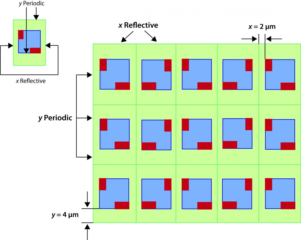
A fast field solver, such as Calibre xACT 3D, can be used to apply boundary conditions on a bit cell (Figure 1). By specifying a closed boundary for the cell, the designer can improve parasitic extraction and simulation accuracy, as well as performance for a symmetric design. Using boundary conditions, bit cell geometries are effectively modeled as a reflected or periodic repeated pattern on all sides of the boundary, at the same distance. This allows the designer to extract a single bit cell accurately without having to construct an array.

This modeling technique enables designers to radically speed up their characterization process and realize a design that performs to their specification. For example, using Calibre xACT 3D, we extracted a bit cell in 4 seconds, whereas a popular reference-level field solver required 2.15 hours. The total capacitance of the nets extracted from the bit cell compared very closely to the reference results.
Using fast field solver technology like Calibre xACT 3D at all stages of memory design, from bit cell design to full chip sign-off, ensures a robust design that will work to specification when it is manufactured.
To read the complete white paper, click here.
 Leave a comment or contact Claudia Relyea if you would like to discuss how Calibre xACT 3D can help your company ensure the successful and timely development of high-performance, low-power memory designs at advanced nodes.


Comments
There are no comments yet.
You must register or log in to view/post comments.