100X800 Banner (1)

Apache on the Road

Apache on the Road
by Paul McLellan on 10-19-2011 at 2:01 pm

There are lots of places that Apache is going to popping up in the next few weeks.

Firstly, Andrew Yang will deliver the keynote on October 24th at the Electrical Performance of Electronic Packaging and Systems (EPEPS) in San Jose. He will be talking about “Chip-Package-System convergence: bridging multiple disciplings to solve low power, cost down and system reliability challenges.”

And the following day at EPEPS, Dr Dian Yang (TIL there are two Dr Yangs at Apache) is on a panel session about the main challenges of high-speed packaging and interconnect.

You can register for EPEPS here.

If EPEPS isn’t your thing, then how about the ARM Techcon 2011. It takes place from 25-27th October in the Santa Clara convention center. The 25th is chip design day (the other two days are dedicated to system and software) and Apache will be participating.

And if Santa Clara is not your thing, ARM Techcon is in Hsinchu on November 18th and in Paris on December 8th.

Next up is MEPTEC (Microelectronics Packaging and Test Engineering Council) conference on “2.5D, 3D and beyond” on November 9th in Santa Clara. I’m looking for the low-down on packaging in the fourth dimension! Aveek Sarkar will be presenting on “Thermal power distribution and reliability interactions in 2.5/3D packaging-modeling.”

And finally, for today, if you are in China in December, the IEEE Electrical Design of Advanced Packaging and Systems (EDAPS) is taking place December 12-14th in Hangzho. Apache will be presenting. More details later.


SICAS capacity data loses TSMC and UMC

SICAS capacity data loses TSMC and UMC
by Bill Jewell on 10-19-2011 at 10:26 am

SICAS (Semiconductor Industry Capacity Statistics) has released its 2Q 2011 data with significant changes in membership. The data is available through the SIA at: SICASdata The SICAS membership list no longer includes the Taiwanese companies Nanya Technology, Taiwan Semiconductor Manufacturing Company Ltd. (TSMC) or United Microelectronics Corporation (UMC). These companies had been in previous SICAS data for several years. Nanya is a relatively small semiconductor manufacturer with revenue of $1.8 billion in 2010. TSMC and UMC are the two largest semiconductor foundries, with 2010 revenues of $13.3 billion and $4.0 billion, respectively. IC Insights, which includes foundries in its rankings of semiconductor suppliers, listed TSMC as the third largest semiconductor supplier in both 2010 and 1[SUP]st[/SUP] half 2011. UMC was 19[SUP]th[/SUP] in both rankings. ICInsights Rankings

The only other change in SICAS participants is the omission of National Semiconductor. The National data may be included with Texas Instruments, which acquired National effective September 27, or may have been neglected during the transition. National’s revenue for its fiscal year ended May 2011 was $1.5 billion.

We at Semiconductor Intelligence estimate TSMC and UMC represented about 16% of total IC capacity in SICAS. Thus losing these companies has caused a major disruption in SICAS data and makes comparison ofthe 2Q 2011 data with previous quarters invalid in most categories. However TSMC and UMC release information on wafer capacity and shipments in their quarterly financial releases. Thus adding the reported TSMC and UMC 2Q 2011 data to the SICAS data results in total IC data which is more comparable to prior quarters.

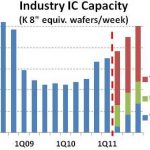
The chart below shows SICAS data for total IC capacity in thousands of eight-inch equivalent wafers per week. Capacity for TSMC and UMC was added to the SICAS 2Q 2011 capacity for comparison with prior quarters. 2Q 2011 IC capacity (including TSMC and UMC) was 2,084 thousand wafers, up 1.6% from 2,052 thousand in 1Q 2011 and the fifth consecutive quarterly increase. IC capacity in 2Q 2011 was still 6% below the record capacity of 2,223 thousand wafers in 3Q 2008. The adjusted 2Q 2011 data is still not entirely comparable to prior SICAS data since Nanya (and possibly National) are no longer participating.

The March 11, 2011 Japanese earthquake and tsunami also had some impact on capacity. The disaster affected several wafer fabs either through direct damage or through power outages. Since SICAS data is based on average capacity throughout a quarter, the impact on 1Q 2011 SICAS data was not likely significant. Most of the affected fabs were back to full production by the end of April. Almost all of the fabs were back up by mid July. Although the size of the impact is difficult to estimate, 2Q 2011 capacity and utilization would have been somewhat higher if not for the Japan disasters.

SICAS reported total IC capacity utilization of 92.2% in 2Q 2011, down 2.0 percentage points from 94.2% in 1Q 2011. The change in participants makes the 2Q 2011 SICAS data not directly comparable to 1Q 2001. Adding capacity and shipment data for TSMC and UMC in 2Q 2011 enables a more apples-to-apples comparison. In this second case, total IC capacity utilization was 92.8% in 2Q 2011, down 1.4 points from 1Q 2011. Another way to make a more equivalent comparison is to use SICAS data for MOS IC capacity without foundry wafers. This category was not as affected by the participant changes since TSMC and UMC reported in the foundry category. Utilization for MOS ICs without foundry was 92.4% in 2Q 2011, down 1.2 points from 93.6% in 1Q 2011.

Thus industry total IC capacity utilization dropped in 2Q 2011 from 1Q 2011, but not by the 2 points indicated by the SICAS data. If the same participants were in both 1Q and 2Q data, the utilization drop probably would have dropped by about 1.2 to 1.4 points. IC capacity utilization has been above 90% for six consecutive quarters following the 2008-2009 downturn.

The change in participants in SICAS is disappointing. SICAS has enjoyed fairly high participation rates since it was formed in 1995. As a member of the SICAS founding executive committee I remember the spirit of cooperation as foundry companies and integrated device manufacturers were willing to share data for the first time, with the goal of providing useful information for the entire semiconductor industry.


Apple is Giving Samsung Semiconductor A Splitting Headache

Apple is Giving Samsung Semiconductor A Splitting Headache
by Ed McKernan on 10-18-2011 at 5:00 pm

Vertical integration, as I have noted in previous blogs, is the way to domination and maximum profitability. That is unless someone else has beaten you to the punch with an even bettermodel. Apple is now executing a product and manufacturing supplier strategy that will force Samsung to lose lots of money and then ultimately split the Semiconductor Group from the larger Samsung Corporate Umbrella. Apple owns the Commanding Heights of the new Computer Ecosystem and has mapped out the more profitable Virtual Vertical Manufacturing Structure that allows it to invest just a portion of the CapEx that traditional suppliers require. Hence, they are growing in profitability at a greater rate than traditional vertically integrated companies. Samsung will need to split off its Semiconductor Unit soon or they will face even greater losses because they will be put in an untenable situation by Apple’s soon to be executed actions.

Most of my recent blog posts have been focused on Apple for one reason. They are re-writing the book on how to run a superior company, from products to manufacturing, and this is having a dramatic impact in the semiconductor industry playing field. Many people focus on the products – which are outstanding. But the other side of the house is cranking on a model that will dramatically increase profit margins at the expense of a multi-sourced supplier base that will ultimately succumb to their wishes (any of their wishes). The readers must understand that Apple can punish as well as incentivize suppliers at their choosing. As I outlined in a blog a few weeks ago Apple is the “swing consumer” of the semiconductor industry (see Apple Plays Saudi Arabia’s Role in the Semiconductor Market). Therefore, they dictate market pricing for many components.

As many of our readers are aware, Apple started a legal process several months ago to keep Samsung Tablets out of worldwide markets because the product looked similar to the iPAD. Samsung is the only company in the world that can challenge Apple on a vertical cost basis and they have the added advantage of having corporate subsidies. Apple’s goal in the coming year is to make Samsung retreat from the consumer market and back into semiconductors or risk losing an excessive amount of money.

The Global Semiconductor market is going through some softness as of late. However, DRAM is very sick and NAND is doing just OK – overall. The picture, I contend, is different if we look vendor by vendor. In a downturn, the largest semiconductor vendor with the biggest CapeEx gets hit worse than the smallest guy. So Samsung is now feeling maximum pain.

Recently, Apple let it be known that it was shifting DRAM and NAND out of Samsung to Toshiba and Elpida. Here’s where it gets interesting. Apple, as recently discussed, has over 70% gross margins in its iPhone 4S so they can afford to pay a little more to certain suppliers that they seek to gain favor with at the expense of a “Bad Supplier.” I contend that Apple is probably paying higher ASPs to Toshiba and Elpida in the short run to get more of their capacity and to penalize Samsung. Samsung is now looking at reduced demand and the prospect of selling out DRAM and NAND at a lower ASP to the gray market. Remember in down times, gray markets have ASPs substantially below contract price. A lot of bleeding is going on. (see Samsung Sees Weaker Earnings)

From a long-term point of view, it is difficult for Samsung to plan for new fabs if they don’t know how much demand they can expect from Apple. And now, Apple is raising the competitive profile of Toshiba and Elpida at Samsung’s expense. If Samsung gets out of the Tablet and Phone market, then that will free Apple to expand into the 25% of the market (phones) that will be like green fields with 70%+ gross margins. And all this occurs by just paying Toshiba and Elpida a few extra cents per part.

Splittsville Time is Approaching.


USB 3.0 PHY Verification: how to manage AMS IP verification?

USB 3.0 PHY Verification: how to manage AMS IP verification?
by Eric Esteve on 10-18-2011 at 6:38 am

Very interesting question from Zahrein in this thread: “how to manage an embedded USB 3.0 PHY Verification”? To clearly position the problem, Zahrein need to run the RTL verification of a complete SoC integrating an USB 3.0 function, that is the Controller (digital) and the PHY (Analog Mixed Signal) embedded in the SoC. The question, as asked by Zahrein, is “inside the USB3 block, we will have a lot of Mixed signals and hence the AMS verification is needed but as a USB3 block connect to the core or IP’s, do we need AMS verification. I believe the Full chip RTL validation would cover it as the Data_In and Data_out is in digital waveform”.

In fact the answer is “No”, you don’t need to run AMS verification at this stage (RTL of the complete SoC), but, immediately comes a condition: as far as the PHY-specific Mixed Signal verification has been done already, and this should be part of the PHY development methodology. The next question quickly comes: is the PHY developed internally, or has it been sourced from an IP vendor? If the latest is true, the solution is not far away.

According with Navraj Nandra, Director for AMS IP at Synopsys: “after integration of the PHY into the ASIC, USB3.0 functional (logical) verification must be done at a “system level” including at a minimum, the PHY, the link-layer controller (host/device, etc.), and any VIPs. For functional verification, Synopsys ships a verilog simulation model in which the digital-logic portion of the PHY is represented by flattened GTECH netlists, and the analog portions of the PHY are represented by behavioral verilog. This verilog model can then be dropped into a simulation bench in which the other elements (e.g. link-layer controller, VIPs, etc..) are instantiated, and functional scenarios can be simulated.”

In other word, the customer doesn’t need to run AMS verification, the PHY is represented by behavioral Verilog model, and you can run a complete “digital-only” verification.

Now, if the PHY has been internally developed, the above methodology can be applied, at the condition that the PHY development team has run PHY-specific Mixed Signal verification, and generated RTL simulation model (digital-logic portion of the PHY represented by flattened netlists, and the analog portions of the PHY are represented by behavioral RTL).

In the “make versus buy” problematic, it shows that the internal PHY development team should behave exactly as an IP vendor, offering the same level of service. As a side remark (here I remember the time where I was doing SoC integration, including AMS and digital functions being provided by different design team within the company) such a “service” can be more difficult to obtain when you are an internal customer than when you are paying a license fee to an IP vendor…

Let’s imagine now that we are doing engineering in the real life (the place governed by the laws of Physics, as well as Murphy’s laws). The above described methodology has been deployed, you have run RTL simulation, and you feel that a scenario is not working quite as expected, and narrows it down to the PHY level. If the PHY has been sourced to Synopsys, Navraj’s suggestion is that the customer:

(a) captures VCD waveforms for this scenario just at the top-level of the PHY,
(b) Open a Synopsys Solvnet case for this, and upload the waveforms on the Solvnet case.


As part of Synopsys customer support, they’ll review it and determine what the problem is.

If the PHY has been internally sourced, there is certainly a similar solution, involving the PHY development team and AMS verification, but the important point here is that the SoC integrator doing RTL verification at the chip level (or below) should not be involved in AMS-level verification.

Hope this answer to Zahrein’s question…

Any comment from the design community is welcomed, as well as mentioning any other approach working for such a scenario!

Eric Esteve from IPNEST – Table of Content for “USB 3.0 IP Forecast 2011-2015” available here


Mentor at the TSMC Open Innovation Platform Ecosystem Forum

Mentor at the TSMC Open Innovation Platform Ecosystem Forum
by Daniel Payne on 10-17-2011 at 3:14 pm

EDA companies and foundries must closely collaborate in order to deliver IC tool flows that work without surprises at the 40nm and 28nm nodes.

Tomorrow in San Jose
you can attend this 4th annual event hosted by TSMC along with Mentor Graphics and other EDA and IP companies.

Here are some of the topics that will interest IC designers using Mentor tools:

iLVS: Accessible, Supportable Paradigm for Circuit Verification at Advanced Nodes (2:30PM, EDA Track)
Accurate, comprehensive device recognition, connectivity extraction, netlist generation and, ultimately, circuit comparison becomes more complex with each new process generation. The number of layers and layer derivations are increasing and the complexity of devices, especially Layout Dependent Effects (LDS), becomes harder and harder to model. In the past, customers could take a foundry rule deck and easily modify it to include their own device models for transistors, resistor, capacitors, inductors, etc., and even augment the deck with their own checks. At 40nm, 28nm, few customers are able to do this confidently. To address this situation, TSMC and Mentor Graphics will discuss how they collaborated to define iLVS, a syntax that provides customers with a more easily adaptable solution to their circuit verification needs. Using iLVS, users can more easily modify and augment foundry rule decks, yet still adhere to the modeling and manufacturing intent captured in these decks.

Keys to Successful DFM Partnership (4:00PM,IP/EDA/Services Track)
DFM is now a known necessity for advanced nodes. But a successful DFM strategy is more than a “push button” solution. It depends on a synergistic combination of tool technology and design methodology, and close collaboration with the foundry. In this session, CSR and Mentor will relate their personal experiences with DFM, its implementation in the TSMC ecosystem, discuss critical factors that determine the difference between success and failure in actual practice.

Challenges and Directions for Next Generation 3D-IC (4:30PM, EDA Track)
The IC industry is steadily moving to the third dimension of scaling, i.e., stacking die vertically using through silicon vias (TSVs) to make inter-die connections in a manner analogous to copper vias in multi-layer printed circuit boards (PCBs), but on a much smaller scale. The 2.5D interposer solution is here today, but next generation, ergo full 3D, will bring additional complexities. For example, when TSVs are introduced into the active area of an IC, things get complicated due to complex electrical, mechanical stress and thermal interactions that impact circuit performance and reliability. In this session Qualcomm and Mentor Graphics will discuss some of the challenges of designing 3D-ICs and what the ecosystem is doing to provide the needed methods and tools to make next generation 3D-IC a reality.

Improving Analog/Mixed Signal Circuit Reliability at Advanced Nodes (5:00PM,IP/EDA/Services Track)
Preventing electrical circuit failure is a growing concern for IC designers today. For certain types of failures such as Electrostatic discharge (ESD) issues, there are well established best practices and design rules that circuit designers should be adhering to. Other issues are more recent, such as the best way to design circuits that cross different voltage regions on a chip. While these topics are not unique to a specific technology node, in particular for analog mixed signal they become increasingly critical as the oxides get thinner for the most advanced nodes and as circuit designers continue to put more and more voltage regions on-chip. To validate that circuits have robust protection from electrical failure, TSMC and MGC will present how they have partnered to define and develop rule decks that enable automatic advanced circuit verification to address these issues at the 28nm and 40nm nodes.

Information on the TSMC Open Innovation Platform Ecosystem Forum is here.


EDA and ITC

EDA and ITC
by Daniel Payne on 10-17-2011 at 10:44 am

Every SOC that is designed must be tested and the premier conference for test is ITC, held last month in Anaheim, California.

I spoke with Robert Ruiz of Synopsys by phone on September 21st to get an update on what is new with EDA for test engineers this year. Robert and I first met back at Viewlogic when Sunrise was acquired in the 90’s.

The Big Picture
Over the years Synopsys has built and acquired a full lineup of EDA tools for test and they call it synthesis-based test:

Scan Test is a very well known technique and designers can choose either full-scan or partial-scan using the TetraMAX tool (technology initially acquired from Sunrise).

The STAR Memory System is technology acquired from Virage and it is well received in the industry with some 1 billion chips containing this IP to date.

Test engineers have a few choices with EDA tools, either buy from one vendor or from multiple vendors where you stitch the point tools together:

Questions and Answers
Q: With smaller process nodes there is more chance for Single Event Upset (SEU) in memories. How do you design for that?
A: SEU is mitigated by using Error Correcting Coding at the design stage.

Q: BIST is a popular test approach, but how do you know that your test electronics is OK?
A: The test electronics is treated like other parts of the logic design, and we add it to the scan chain too.

Q: Where would I use your Yield Analysis tool?
A: Within a foundry for example on the initial yield of new nodes there may be low yield, so this approach helps them find out where on each design the yield is being limited.

Q: Who else would use Yield Analysis?
A: We see users in IDM, Foundries and Fabless wanting to improve yield with this tool.

Q: How does static timing analysis work with ATPG?
A: In our test flow Static Timing Analysis (Prime Time) can guide TetraMAX (ATPG) for critical paths and area defects. Slack info sent to TetraMAX that will uncover any timing defects.

Q: Do temperature gradients cause speed faults?
A: Yes, and you could uncover any speed fault with our tools.

Q: What kind of Market share does Synopsys have in the EDA test tools?
A: Mentor and Synopsys are the top two suppliers for DFT tools. The top 20 semi companies roughly split in DFT between SNPS and MENT.

Q: Was Mentor Graphics the first to offer compression tools for test?
A: Yes, however our compression is more efficient compared to their approach.

Q: How are Synopsys test tools different from Mentor or Cadence tools?
A: The design flow using our logic synthesis is the biggest difference. For Memory and IO testing we lead in this IP (through Virage).

Q: Can scan compression create routing issues like congestion?
A: Yes, here’s a graphical comparison of routing congestion – white and red are high congestion in routing. Optimization for removing congestion is shown on the right-hand side. At synthesis stage any congestion will make the physical design tool run times much longer, or even fail to complete. Smart synthesis tools can help on congestion so that P&R times are quicker.

Q: What kind of industry endorsements do your DFT tools have?
A: We’re in the TSMC Reference flows.

Q: What are some pitfalls during test?
A: During test your chip may draw more power than in the budget (red is too much power), and that can damage the device during scan testing. Users can define their power budget during testing using DFT tools (green shows the budget), lower power can mean longer run times. This is a mature technology and it doesn’t require extra DFT up front (DFTMAX has compression).


SIG feedback – 19[SUP]th[/SUP] annual event this past Monday, tech papers presented. Samsung presented in 2010 for reduced tester power consumption.

Q: What’s happened after the Virage acquisition?
Q: Synopsys had a relationship with Virage before acquisition. Now the DFT tools know the scan chains and can connect memory scan to logic scan more efficiently. We can even re-use shift registers as scan elements, saving area up to 10% based on design style.

We can model memories with scan chains embedded, then optimize the ATPG runtimes. Use the Virage memories and Synopsys ATPG for the best test results.

Q: How do I optimize the number of scan chains?
A: Our tools let you optimize that.

Q: What is Yield Explorer all about?
A: This tool reads silicon data that is failing scan tests.

  • – Accept physical design info and know where the defect is occurring (this via, that cell)
  • – Also useful for volume diagnosis.
  • – Defects today can be subtle, beyond just stuck-at faults, more cross-talk induced errors or noise errors.


This can help get to a higher yield quicker. Use the defective silicon data to help diagnose and pinpoint where to find failures. Create a candidate list of where to look. Designers can become more involved on where the failures are located at.

Q: How can you find and then verify IC defects?
A: Use etching techniques to find it visually. Yield analysis will pinpoint to the cell level what is suspect.

Q: Who is using this Yield Analysis capability?
Q: One customer is ST Ericsson who presented at SIG on Monday, they ran the Yield Explorer with TetraMAX and immediately found a via causing loss. They then made one design change, and yield went up 47%. They used the LEF/DEF feature to reduce area to look for loss. Fewer scripts to glue tools together.

Q: Yervant Zorian, tell me about Virage within Synopsys now.

A: We started 10 years ago to offer Memory test automation, and are now in our 4[SUP]th[/SUP] generation of memory test with some 1 billion chips using the Virage approach. The percentage of SOCs using RAM can be 60% now, so memory yield can limit the chip yield. Power is an issue during the testing of RAMs so you have to be intelligent about how to test these without exceeding limits.

In our IP with BIST the DFT tools used by the designer can analyze the results all the way down to the physical level.

The diagnosis of chips through JTAG ports allow the debug of all memories on the SOC in a low-cost fashion.

One challenge is how to diagnose SRAMs early in a new node that is just being defined. With Yield Analysis you can now use an automated approach to help improve yield for this.

All of our memory IP requires extensive characterization before it gets placed in a new SOC.

Summary
Synopsys offers a full suite of DFT tools and testable IP used by both design engineers and test engineers. The dominance of Design Compiler for logic synthesis is what makes the Synopsys tools different from the other vendor offerings.


TSMC Gets Fooled Again!

TSMC Gets Fooled Again!
by Daniel Nenni on 10-16-2011 at 2:51 pm

If you follow the SemiWiki Twitter feed you may have noticed that The Motley Fool (Seth Jayson) did three more articles on TSMC financials. The first Foolish article was blogged on SemiWiki as “TSMC Financial Status and OIP Update”.

The next three Fool Hardy articles look at cash flow (the cash moving in and out of a business), accounts receivable (AR), days sales outstanding (DSO) and a closer look at margins. All three articles are interesting reads so if you have the time I would definitely click over. If not, here are the cool pictures and my expert guess of the foundry business going forward.
Don’t Get Too Worked Up Over #TSMCEarnings http://www.fool.com/investing/general/2011/10/04/dont-get-too-worked-up-over-taiwan-semiconductor-.aspx

Over the past 12 months, Taiwan Semiconductor Manufacturing generated $687.4 million cash while it booked net income of $5,543.0 million. That means it turned 4.5% of its revenue into FCF (Free Cash Flow). That sounds OK.

However, FCF is less than net income. Ideally, we’d like to see the opposite. Since a single-company snapshot doesn’t offer much context, it always pays to compare that figure to sector and industry peers and competitors, to see how your business stacks up.

With questionable cash flows amounting to only -1.1% of operating cash flow, Taiwan Semiconductor Manufacturing’s cash flows look clean. Within the questionable cash flow figure plotted in the TTM period above, changes in taxes payable provided the biggest boost, at 1% of cash flow from operations. Overall, the biggest drag on FCF came from capital expenditures, which consumed 92.2% of cash from operations.

DanielNenni SemiWiki.com
#TSMCPasses This Key Test fool.com/investing/gene…

Sometimes, problems with AR or DSO simply indicate a change in the business (like an acquisition), or lax collections. However, AR that grows more quickly than revenue, or ballooning DSO, can also suggest a desperate company that’s trying to boost sales by giving its customers overly generous payment terms. Alternately, it can indicate that the company sprinted to book a load of sales at the end of the quarter, like used-car dealers on the 29th of the month. (Sometimes, companies do both.)

Why might an upstanding firm like Taiwan Semiconductor Manufacturing do this? For the same reason any other company might: to make the numbers. Investors don’t like revenue shortfalls, and employees don’t like reporting them to their superiors.

Is Taiwan Semiconductor Manufacturing sending any potential warning signs? Take a look at the chart above, which plots revenue growth against AR growth, and DSO. Will Taiwan Semiconductor Manufacturing miss its numbers in the next quarter or two? I don’t think so. AR and DSO look healthy. For the last fully reported fiscal quarter, Taiwan Semiconductor Manufacturing’s year-over-year revenue grew 5.3%, and its AR dropped 3.9%. That looks OK. End-of-quarter DSO decreased 8.7% from the prior-year quarter. It was down 4.9% versus the prior quarter.
DanielNenni SemiWiki.com
Are You Watching This Trend at #TSMC? fool.com/investing/gene…

Margins matter. The more Taiwan Semiconductor Manufacturing (NYSE: TSM ) keeps of each buck it earns in revenue, the more money it has to invest in growth, fund new strategic plans, or (gasp!) distribute to shareholders. Healthy margins often separate pretenders from the best stocks in the market. That’s why we check up on margins at least once a quarter in this series. I’m looking for the absolute numbers, comparisons to sector peers and competitors, and any trend that may tell me how strong Taiwan Semiconductor Manufacturing’s competitive position could be.

Here’s the margin picture for Taiwan Semiconductor Manufacturing over the past few years:

Here’s how the stats break down:

  • Over the past five years, gross margin peaked at 49.4% and averaged 45.8%. Operating margin peaked at 40.1% and averaged 35%. Net margin peaked at 40% and averaged 34.5%.
  • TTM gross margin is 48.7%, 290 basis points better than the five-year average. TTM operating margin is 36.9%, 190 basis points better than the five-year average. TTM net margin is 36.5%, 200 basis points better than the five-year average.

With recent TTM operating margins exceeding historical averages, Taiwan Semiconductor Manufacturing looks like it is doing fine.

My expert guess is that the semiconductor industry will continue to struggle as a result of the economic uncertainty around the world. Unemployment, debt, housing crisis, over population (7 Billion+ people!); consumers will spend less money on electronics next year. To make things worse, semiconductor inventories are at pre-recession levels. In Q2 2011, the DOI (days of inventory) reached 83.4 days, exceeding the last record high of 83.1 days seen in the first quarter of 2008. The good news is that smart phones are no longer considered a luxury, smart phones are now life lines which means they will continue to hyper drive the semiconductor industry for years to come. China is hugely subsidizing mobile phones and India launched a $35 tablet ($60 cost) so the internet will be coming before indoor plumbing in some regions.

In regards to TSMC, it is all good news. Take a look at the charts and you will see an extremely healthy company in a VERY competitive market and the MOST economically challenging times the semiconductor industry has ever seen. TSMC has already won the 28nm node and 20nm is not far behind. TSMC is easily a $20 stock, believe it.

UMC botched 40nm and is struggling with 28nm, this really breaks my heart as I absolutely respect the UMC engineers. SMIC was a huge disappointment. Backed by the Chinese government and the largest domestic market for consumer electronics, how could they fail? But fail they did. Hopefully the recent re-org will get SMIC back in the foundry game! I also had high hopes for GlobalFoundries as a competitive threat for TSMC. GFI is actually doing quite well, unfortunately we all got carried away in the excitement and unachievable expectations were set. Intel 22nm may be the only real threat to TSMC at 28nm and it will certainly be exciting to see how that all plays out.


Austin and San Jose SCC

Austin and San Jose SCC
by Paul McLellan on 10-14-2011 at 3:35 pm

Don’t forget the SpringSoft Community Conferences next week in Austin on Tuesday and in San Jose on Thursday. There is no charge and you even get a free lunch (see “no such thing as…”).

The morning in Austin is focused on functional closure and how to leverage SpringSoft’s verification technology around Verdi and Certitude and the new ProtoLink Probe Visualizer for FPGA debug. The afternoon is focused on custom IC design and how to get better results using the Laker custom IC technology.

In San Jose this order is reversed, with the morning being dedicated to custom IC design and the afternoon to functional verification.

Registration for both SCC conferences is here.


Soft IP Qualification

Soft IP Qualification
by Paul McLellan on 10-14-2011 at 3:10 pm

At the TSMC Open Innovation Platform Ecosystem Forum (try saying that three times in a row) next week (on Tuesday 18th), Atrenta will present a paper on the TSMC soft IP qualification flow. It will be presented by Anuj Kumar, senior manager of the customer consulting group.

More and more, chips are not put together what we think of as the standard way, by writing a bunch of RTL and then going through “classic” EDA. Instead, they are assembled out of pre-existing IP, either from the 3rd party IP marketplace or from a previous chip in the same company. So the focus of what is important in a design has to change. On many chips the IP content is well over 80%, and a lot of that is in the form of soft IP blocks (aka synthesizable IP). So it is essential that designers know the quality of the IP and any integration risks associated with using it. This information is crucial to making sure that an SoC meets its power, performance, area (price) and schedule.

Atrenta has been collaborating with TSMC to create a comprehensive system to automate the process of IP qualification. Of course this is based on the SpyGlass platform. The system analyzes soft IP using an IP handoff methodology consisting of TSMC’s Golden Rule Set covering various design parameters for the soft IP block: risk analysis, integration readiness, implementation readiness and reusability.

Information on the TSMC Open Innovation Platform Ecosystem Forum is here. Atrenta will be presenting at 1pm on Tuesday October 18th.


Conclusion of the USB 3.0 IP forecast from IPNEST… complimentary for SemiWiki readers

Conclusion of the USB 3.0 IP forecast from IPNEST… complimentary for SemiWiki readers
by Eric Esteve on 10-14-2011 at 10:40 am

Using the “Diffusion of Innovation” theory, we have built a forecast for the market of USB 3.0 IP in 2011-2015. In this new version of the report, we have inserted the actual revenues generated by USB 3.0 IP from different vendors, for 2009 and 2010, and reworked the 2011-2015 forecast. Initially, we had expected this IP market to ramp up very fast, because the USB technology is already familiar to the end user, so the market adoption should be easier than for other emerging technology. In fact, the ramp-up is not as fast as expected, and the reason is crystal clear: even if the technology is already available and demonstrated in applications like external storage, the most important enabler was missing: the availability of PC or Notebook with native SuperSpeed USB support, or USB 3.0 included in the PC chipset. Because the electronic industry is expecting such an introduction to come in Q2 2012, and PC shipments to follow quickly and reach a rate greater than 80% during 2013, the sales for USB 3.0 IP are breaking a barrier: after “Innovators” and “Early Adopter”, USB 3.0 is expecting to reach “Early Majority” starting in 2012. Because of the SoC design cycle, IP sales are happening now, at OEM designing for Consumer Electronic and other mass market applications.

In order to build an accurate forecast for IP sales, we have used a bottom-up methodology. Usually, the top down approach is followed: based on an expected count of design start by market segment, you try to determine (using a secret sauce?) the proportion of designs where a certain technology will be used. For an emerging technology like USB 3.0, we have preferred an approach which is to review all the Applications (in all the market segments: PC, PC Peripherals, Consumer Electronics and Wireless handset), evaluating the list of actors (OEM, IDM, Fabless) for each Application, and determine if they will adopt USB 3.0 and, even more important, when they will do it. We have clearly identified a first wave of applications, where the adoption of SuperSpeed USB was fast: External Storage (HHD before SSD) and a very few PC Peripherals (Bridge, Hub, Web Camera…). The end user should be highly motivated, as he had to use a PCIe to USB 3.0 bridge (HBA or ExpressCard), to move to USB 3.0.

The second wave of Applications is starting to generate IP sales now, for products to be launched in 2012 and later and to be connected to PC integrating PC Chipset with native USB 3.0 support. These are, in CE segment: Set Top Boxes, DVD and Blue-Ray, HDTV, then Digital Video Camera before Digital Still Camera, in PC Peripherals segment: LCD PC Monitors, HDD Enclosures, External SSD and me-too ASSP for bridges and hubs and in Wireless handset segment the Application processors for smartphone. This second wave should represent a jump in USB 3.0 IP sales, breaking the 100 barrier during 2012 or 2013.
The third wave of Application could be linked to the “Late Majority” from the Innovation theory, and should start to hit the market in 2014, when more than 90% of the PC will be shipped with USB 3.0. We have listed all these applications and evaluated the number of additional USB 3.0 IP sales associated to be lower than for the second wave, but significant, so the USB 3.0 IP market in 2015 should weigh as much as the overall USB IP market in 2010.

If we consolidate the USB 3.0 IP with the existing USB IP market, the total USB IP market should be in the range of $55-60M in 2010. In other words, USB is still the largest of all the Interface IP markets (HDMI, PCI Express, SATA and DDRn) at that date, as we have shown in (4). But probably not for so long, as DDRn and HDMI (thanks to the royalties) IP markets are growing faster than USB. SuperSpeed USB has been introduced late in the market, compared with HDMI, PCIe gen-2 or SATA 3G. During this delay the end users have learned to use other protocols to interface a device to a host, this versatility has probably impacted the potential for USB 3.0 pervasion, and the related USB 3.0 IP sales.

This is the conclusion from the “USB 3.0 IP Forecast 2011-2015”. But as you now, “devil is in the details”, and you will find many details in this 48 pages survey –unique on the market- exclusively dealing with IP. Take a look at the Table of contents here.

Eric Esteve – CEO IPNEST