
For the 20[SUP]th[/SUP] anniversary of IP-SoC, we had about ten presentations, most being really interesting; the conference has provided globally a very good level of information, speakers coming from various places like China, Belarus, The University of Aizu (Japan), University of Sao Paulo (Brazil), Silesian and Warsaw University of Technology (Poland), BNM Institute of Technology (Bangalore-India) and obviously from western Europe and USA. I am going to IP-SoC for more than five years now, and I am glad to see that there is no more room for the insipid “marketing” presentation that some IP vendors used to give. It was real information, and if you were attending to presentation focused on security, like this given by Martin Gallezot (one of my former colleagues at PLDA), you really needed to know a bit on the topic (Physical Attacks against Cryptographic) to fully understand… but that’s exactly what you expect when you go to a conference, isn’t it? Learn something new for you.
And, obviously, doing networking within this niche part of the industry which is IP. IP-SoC was the right place to network, and I did it as much as possible, as well as finding new customers in the IP vendor community. Sorry, I can’t give you names; we need to close the deal first!
Starting with the 20th anniversary Special Talk, we had (as usual) a « Semiconductor design IP Market overview » from Gartner ; if you remember my blog in January about Gartner, they were very good at forecasting… the past. This year, Gartner has improved, as they are now giving a year-to-year design IP revenue growth forecast of 10% for 2011, 4% for 2012, and 8% for 2013 and later, which is more on line with what we can expect from the IP market, compared with the few % they gave last year. Also interesting, the result of a survey made by Gartner with the IP consumer. In particular:
- To the question: “What are the most important criteria to select a specific IP?” 90% have answered “It must be Silicon provenand tested”.
- To the question: “Why do you use design IP?” 70% have answered “To improve Time-To-Market”.
Nothing surprising in these answers, but rather the confirmation that it’s really difficult to enter the IP market, as even if your product is wonderful, it will not be silicon proven, and the first sale will be very difficult to make!
The conclusion from Gartner was, at least to my opinion, rather funny: “78% of the semiconductor growth in 2012 will come from Smartphone and Media Tablet; so you should sell on this market”. Funny, because if you are not selling on this market, it’s probably too late in December 2011 to modify your port-folio to attack it in 2012…
Last information you may value: IP market weighted $325M in 1998, and weights now $1.7B; this represent 0.12% of the value of the End Equipment served by these IP; impressively low, isn’t it?
Another presentation http://www.design-reuse.com/ipsoc2011/program/ was by Marc Millerfrom Tabula. I know Tabula (and Marc) since 2005, when we decided at PLDA to support them with our PCI Express IP. At that time, only a few people did really understood what exactly their product was. I think in the meantime, a lot more people understand Tabula new concept, based on “dynamically reconfigurable hardware logic, memory, and interconnect at multi-GHz rates”. That’s a pretty good idea: the same piece of Silicon, say a LUT as we are in the FPGA world, will be used to support different logic functions, within the same system clock period! Two remarks: at first, the Silicon should run as fast as possible, that’s why Tabula has invested into 40nm technology; second remark: how damn can we use the existing design (EDA) tools? The answer is: no way! So, Tabula is 50% an EDA company, designing his own toolset, and 50% a hardware FPGA vendor. According with Marc, the “official” release of the tools is to come very soon, I say “official” as Tabula is already claiming to have customers. Will Tabula successively compete with the duopole? I don’t know, but their product is real innovation!
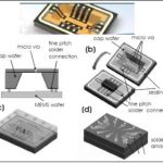
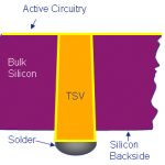
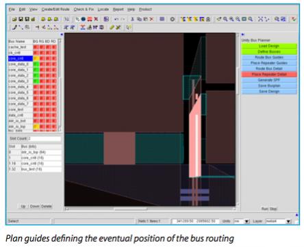
I realize that one blog is too short to cover all the other interesting presentations (cache coherence, 3D-IC for butterfly NoC to name a few), I will have to come back in a second blog. I will just mention… my presentation before leaving you:“ Interface IP Market Birth, Evolution and Consolidation, from 1995 to 2015. And further?”That was the first time I saw people standing during the show, not to leave the room but to better see the slides! Among a few compliments I got after the presentation, one was especially precious to me, as it came from a SC, and even IP, veteran: Jonathan Edwards, now IP Manager at ST-Ericsson. In fact, Jonathan started his career back in the 70’s working with GEC Plessey then INMOS in the UK, and for ST-Microelectronics when they bought INMOS, and has stayed in the technical expertise role all time long. Thanks again Jonathan!
By Eric Estevefrom IPnest– Interface IP Survey available here.