Most of what you see at DAC is canned PowerPoint presentations, however on Tuesday afternoon I spotted a company called Oski Technology that was doing something almost unheard of – they had an engineer debugging a digital design from Nvidia using formal tools live. I later found out the engineer found 4 bugs in just three days without any assistance from Nvidia. Continue reading “Finding RTL Bugs Live Using Formal Techniques”
Electromagnetic Simulation Update from Nimbic
Dr. Raul Camposano, CEO of Nimbic talked with me on Wednesday at DAC to provide an update on what’s new with their electromagnetic simulation tools.
Continue reading “Electromagnetic Simulation Update from Nimbic”
DesignSync update from Dassault Systems at DAC
At DAC on Wednesday Rick Stanton of Dassault Systems gave me an update on what’s new with DesignSync, a design data management tool offered since 1998. Rick and I both worked at Viewlogic in the 90’s along with Dennis Harmon who then founded Synchronicity, later acquired by Dassault Systems.
Continue reading “DesignSync update from Dassault Systems at DAC”
Webinar: how to reduce mobile device cost and board space with LLI
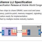
LLI Specification has been officially released by the MIPI Alliance, at the occasion of the Mobile World Congress in Barcelona, this year. As indicated by the name, the round-trip latency of the LLI inter-chip connection is fast enough for a mobile phone modem to share an application processor’s memory while maintaining enough read throughput and low latency for cache refills. Sharing the same DRAM device means the wireless handset integrator can save real estate printed circuit board (PCB) space and create a thinner smartphone, or implement additional device, more features to the smartphone, like NFC chip for example. It also means that the OEM will save, on every manufactured smartphone, the cost of one DRAM ($1 to 2$). If you manufacture dozen of million smartphone like some of the leaders, you can see how quickly you will get the return on the initial investment done by the chip makers to acquire the IP!
MIPI Alliance is strongly supportive of LLI, as we can see from this quote: “As active MIPI contributors, Synopsys and Arteris are aiding in the adoption of the MIPI M-PHY and MIPI Low Latency Interface,” said Joel Huloux, chairman of the board of MIPI Alliance. “The early integration and availability of the Arteris and Synopsys solution helps speed time to market for MIPI LLI adopters.” LLI support from Arteris and Synopsys illustrate how important is to build a strong partnership when selling a complementary solution, as the joint solution consists of Arteris’ Flex LLI™ MIPI LLI digital controller IP and Synopsys’ DesignWare® MIPI M-PHY IP. A team of Arteris and Synopsys engineers, formed to facilitate verification and testing of the joint solution, validated its functionality and interoperability. And for those who love to get insights, you should know that LLI was initially developed by an Application Processor chip maker, who understood that the function, to be successful on the market, has to be marketed and sold by an IP vendor, Arteris was selected as they were already marketing C2C or “Chip To Chip Link” IP, offering exactly the same functionality (sharing a DRAM between Modem and Application Processor), by the means of a parallel Interface, we will come back soon about this IP.
You will certainly get more information by registering and attend this webinar, just go here
Overview of this webinar:
When designing mobile devices, it is critical to implement technologies that will future-proof your design, minimize BOM costs and board space, and maintain or improve performance. The MIPI Alliance Low Latency Interface (LLI) and M-PHY are two technologies that can help future-proof your design while giving it competitive advantages in terms of cost, board space, performance, and time-to-market.
The webinar will present a case study describing how LLI can be used to minimize DRAM footprint on a mobile phone system board. Particular attention will be paid to real-world implementation issues, such as clock domain, power and voltage management as well as integration with SoC interconnect fabrics.
This webinar will teach you:
- What the LLI and M-PHY technologies are, and best practices for implementation
- How LLI is different than other chip-to-chip interface standards, such as USB and PCIe
- How the LLI point-to-point interconnect can benefit multi-chip systems
- How the LLI controller and M-PHY IP can reduce the silicon footprint on your board
- How LLI can reduce individual BOM and multi-product platform costs
Who should attend:
This webinar is targeted at system architects, mobile device and consumer electronics product managers and designers, design engineers, SoC architects, and project managers.
Presenters:
Hezi Saar, Staff Product Marketing Manager, Synopsys
Hezi Saar serves as a staff product marketing manager at Synopsys and is responsible for its DesignWare MIPI controller and PHY IP product line. He brings more than 17 years of experience in the semiconductor and electronics industries in embedded systems. Prior to joining Synopsys, from 2004 to 2009, Saar served as senior product marketing manager leading Actel’s Flash field-programmable-gate-array (FPGA) product lines. Previously, he served as a product marketing manager at ISD/Winbond and as a senior design engineer at RAD Data Communications. Saar holds a bachelor of science degree from Tel Aviv University in computer science and economics and an MBA from Columbia Southern University.
Kurt Shuler, VP of Marketing, Arteris
Kurt Shuler is the VP of marketing at Arteris. He has held senior roles at Intel, Texas Instruments, ARC International and two startups, Virtio and Tenison. Before working in high technology, Kurt flew as an air commando in the U.S. Air Force Special Operations Forces. Kurt earned a B.S. in Aeronautical Engineering from the U.S. Air Force Academy and an MBA from the MIT Sloan School of Management.
Philippe Martin, Vice President, Corporate Applications and Senior Fellow, Arteris
Philippe Martin is Vice President, Corporate Applications and Senior Fellow at Arteris. He has been involved in the development of the MIPI Alliance Low Latency Interface (LLI) specification since the creation of the MIPI Alliance LLI Investigation Group in 2009. Philippe is a renowned expert on LLI and has contributed to the technology through the MIPI Alliance LLI Working Group. Philippe has also participated in the first two commercial implementations by semiconductor companies of the LLI standard.
By Eric EstevefromIPNEST
Laker IC Layout Update at DAC
Taiwan’s most famous EDA company is SpringSoft so on Wednesday at DAC I met wtih Dave Reed, Director of Marketing to get an update on what’s new with their IC layout tools. Continue reading “Laker IC Layout Update at DAC”
Designing a Wafer-Scale Image Sensor for use in X-Rays
At Intel we mused about designing wafer-scale integration (WSI) back in the 70’s however I just learned about how Dr.Renato Turchetta at the Science and Technology Facilities Council (STFC) designed a wafer-scale imaging sensor chip for X-Ray applications. I was also able to interview Dr. Turchetta to learn more about the challenges that they faced in creating this chip.
Continue reading “Designing a Wafer-Scale Image Sensor for use in X-Rays”
Will Microsoft Go Thermonuclear?
Microsoft is in trouble. Many of you already know that. Steve Ballmer has one last opportunity to set the company on a growth path or they will retreat into IBM legacy mode… ala the post 1990s Lou Gerstner era. And so they introduce a large tablet-convertible in direct competition with their PC partners Dell and HP. The End Game is coming sooner than anyone expected. Where is this headed?
A few weeks ago I considered writing a blog following the disastrous Dell quarterly earnings report where they admitted Apple’s iPAD was starting to inflict damage on their PC business. I was sure that this was going to be a forcing function on the Wintel Empire and tried to look at it from the Intel side. Would Intel get into the PC business as Dell and HP scaled back? I couldn’t complete the logic because an Intel entry is at conflict with Apple’s strong consumer push with their PCs.
No, the more logical conclusion is that Intel forges ahead with owning the high performance driven datacenter market (at some ever shrinking expense to HP and Dell) while Microsoft scrambles to replace HP and Dell in the client space where form factors are shrinking dramatically. DVD and HDDs are now being replaced by tiny, energy sipping NAND flash chips while application delivery over the cloud becomes a must.
Then there are the economics to consider but first a little history on tablets:
Microsoft has been dabbling in tablets for more than 20 years. Does anyone remember the flaming startup called Go? The stylus and hand writing recognition were considered the key to tablets taking off and Microsoft thought that they were closing in on a solution year after year. As an engineering friend of mine liked to say on a daily basis about his constantly delayed chip tapeout: “never been closer.”
The aim of hand writing recognition was to enhance Microsoft’s bread and butter Office Application environment with users casually writing in documents on a screen. It was a hard object (stylus) on a hard SURFACE (had to throw that in). It was clunky and unnatural. As is typical to all massively planned grand events, history chooses to take a detour and we ended up with smartphones and tablets controlled by the soft touch of a thumb and index finger.
Now to the Economics:
Apple’s operating margins are now greater than Microsoft (39% vs. 36.8%). Did you know that? If Microsoft stays on the Wintel course in the tablet and PC market working with traditional customers like Dell and HP they will face either shrinking margins or reduced volume to stay relevant. The alternative is to take the hardware into their own hands and deliver a complete solution to corporations and consumers while eliminating costs by going vertical. This is what the tablet announcement signifies and in a way it is leading down the IBM’s mainframe bundled solutions path. Eliminating Dell and HP off the top reduces the end prices of PC equipment by 15-25% depending on the configuration. It’s a good start towards being competitive but without a doubt a burning the ships moment.
Microsoft will need to go a step further and take ownership for some of the silicon that goes into the tablet and ultrabooks. Specifically they will need to acquire the likes of nVidia and AMD in order to develop low cost ARM and x86 processors and thereby effectively moving margins into Microsoft’s pocket. The new vertically integrated Microsoft then can replicate the Apple supply chain enabling them to hit low end market price points and to undercut Intel in the >$700 mobiles that use Ivy Bridge. Now this is a true Thermonuclear War. In the end, the 30 year old Wintel stasis can not coexist with Apple’s hyper growth.
Steve Ballmer has maybe two years (more likely one year) to put Microsoft in a leadership position that remains within spitting distance of Apple. If he is not successful, would it be even possible for Bill Gates to come out of retirement to forge a winning plan?
FULL DISCLOSURE: I am Long AAPL, INTC, QCOM, ALTR
EDA Tools to Optimize Memory Design
I met with Amit Gupta, President and CEO of Solido at DAC on Tuesday to get an update on their EDA tools used in the design of memory, standard cells and low-power. In 2012 they’ve expanded to add three new software packages: Memory, Standard Cell, Low Power. They must be doing something right because at DAC this year I see more competitors jumping into the Fast Monte Carlo space. Continue reading “EDA Tools to Optimize Memory Design”
IC Cell Library Characterization at DAC
Edmond Macaluso, President of Z-Circuit Automation met with me at DAC on Tuesday afternoon to provide an overview of how their EDA tools characterize cell libraries. Continue reading “IC Cell Library Characterization at DAC”
Mike Muller’s ARM Keynote at DAC 2012
Mike Muller’s keynote focused on a lot of changes since the ARM1 was designed in 1983 when ARM the company did not exist and ARM was the next generation processor for Acorn Computer, which was really in the hobby market and had its first boost when they had a contract to design the BBC Microcomputer to go along with a computer literacy project. My minor claim to fame about the ARM1 was that I installed the VLSI Technology design software that was used to design it on two Apollo workstations (which hadn’t actually shipped so I had to go and install it at Apollo not Acorn).
Mike decided to dig up the layout of the ARM1, which turned out to be more of a challenge than expected, involving finding an Exabyte drive, converting VAX files to Linux and converting from CIF (which VLSI Technology used for layout) to GDSII. The original ARMs were full custom designs (this predated synthesis). ARM have recently announced a low end microcontroller, the Cortex-M0. It turns out that this is roughly the same number of transistors as the ARM1 so it makes an interesting basis for comparison.
The chips are about 26 years apart, or 13 process generations, so it should be about 1/2[SUP]13[/SUP] smaller (namely 1/8000) and it is actually 1/10,000 times smaller so about right. Performance should be about 6 performance scalings, so 64 times as fast but it is only 16 times as fast. This is because the 5V power supply that the ARM1 used should have scaled down to 8mV but in fact it has only scaled to 950mV and so the transistor threshold voltages haven’t scaled enough.
The big change in design is that the ARM1 took 6 months to layout. The Cortex-M0 took 32 minutes. Basically synthesis, place and route has automated the whole process whereas the ARM1 was custom. But that is really the only major improvement in design methodology.
Mike then looked at the design productivity. The ARM1 took 6 man-years (MY) and was 25,000 transistors. The dual Cortex-A15 took 150MY and is 150 million transistors. Luckily design productivity has increased 240 times. It is when you look at software that things are scary. The ARM1 graphics library was 0.25MY of work and was 150 lines of code (Loc). Assembly of course. The current ARM GPU, the Mali-T604 has OpenGl, open CL and other graphics support and is 190MY of work and 1M LoC. Just a 7 times increase in productivity.
Mike pointed out that the hardware people shouldn’t be complacent. We came up with synthesis and P&R so that we can essentially compile our chips. But we haven’t come up with anything comparable since. Software people have moved onto Python, cloud computing, development environment and lots of new goodies. So apart from the few people left having to write device drivers, the way software is being developed is changing fast.
Next Mike moved onto validation. The ARM1 was in 3um, had 24,000 transistors and took 6 MY to validate. The Cortex-M0 is in 20nm, 32,000 transistors (not much more) and took 11 MY to validate. But the big difference is the machine resources brought to bear. The ARM1 took 2,000 hours to validate but the Cortex-M0 took 1,439,000 hours to validate. Taking the speed of the machines into account this is 3,000,000 times less efficient. We waste a lot of computer cycles early, especially with constrained random verification, in order to avoid silicon respins later.
Mike feels we need to get more formal design techniques. Today formal verification is stuck on the side of the design process as an “optional extra” to be run by a specialist, rather than something embedded deeply in the design process. Without this we are stuck with constrained random and burning computer and verification engineer cycles, and formal verification not part of every designers job.
As an aside, Mike talked a bit about building ARM’s datacenter in the parking lot. It has 200TFLOPS and 93TB DRAM. It consumes 1.5MW (luckily there was a new housing tract going in across the street so they actually managed to get a line like that installed). The UPS consists of two parts, firstly 6 spinning flywheels which can each deliver 250KW for 20 seconds. Then two 785bhp quad turbo diesel generators that can get up to full power in 8 seconds. Looks pretty good too!
There is a video the keynote here. The video starts with the DAC award session and the keynote itself starts at 29 minutes in. Wait and let enough of the video load and then you can skip straight to the start (unless you really want to see a re-run of the award session).

