Hard to believe EDA360, the Cadence Blueprint toBattle ‘Profitability Gap’; Counters Semiconductor Industry’s Greatest Threat!, is DEAD at the ripe old age of one. As you may have already read John Bruggeman left Cadence after the company conference call last week. The formal announcement should go out on Monday after the SEC paperwork is complete. The question is why?

Richard Georing did a very nice anniversary piece “Ten Key Ideas Behind EDA360 – A Revisit” which is here. Points 1-9 are a good description of what Synopsys and Mentor already do today but they call it revenue instead of a “vision”. Point 10 is the real reason behind EDA360’s failure and JohnB’s departure:
10.No one company or type of company can provide all the capabilities needed for the next era of design. EDA360 requires a collaborative ecosystem including EDA vendors, embedded software providers, IP providers, foundries, and customers.Cadence is committed to building and participating in that ecosystem…..
One of the school teacher comments that has followed me through life is that I “don’t play well with others”, which is absolutely true to this day. The same goes for Cadence, they do not play well with others. That wasn’t always the case of course, but it certainly is today. To borrow a phrase from another SemiWiki Blog, Cadence has a barbed wire fence strategy and EDA360 cannot survive inside barbed wire.
No one will grieve more than me since EDA360was great blogging fodder. My first blog: Cadence EDA360 Manifesto caused quite a stir and got me beers with John Bruggeman. In turn I gave him an EDA360 monogrammed grey hoodie which he actually wore. Calling it a “manifesto” was clearly a PR mistake which they admitted and corrected.

My second blog: Cadence EDA360 Redux! Made fun of the tag line:
“Cadence Design Systems, Inc. (NASDAQ: CDNS), the global leader in EDA360………”
Of course, why wouldn’t Cadence be the global leader in something they just made up? Actually I typed: “Of course, why wouldn’t Cadence be the global leader in something they just pulled out of their corporate butts?” My wife/editor, however, did not like the mental image it created so I changed it. Butt now you know the truth! Cadence PR got rid of that tag line shortly thereafter.
I also blogged TSMC OIP vs CDNS OIP Analysis to point out the error of choosing the same name as TSMC for a similar program:
The TSMC Open Innovation Platform™promotes timeliness-driven innovation amongst the semiconductor design community, its ecosystem partners and TSMC’s IP, design implementation and DFM capabilities, process technology and backend services……
Cadence Design Systems, Inc. (NASDAQ: CDNS), the global leader in EDA360, today announced the Cadence Open Integration Platform, a platform that significantly reduces SoC development costs, improves quality and accelerates production schedules…..

Cadence dropped that one as well. Lawyer letters may have been involved so I cannot take full credit. My Semiconductor Realization!Blog was much more EDA360 supportive:
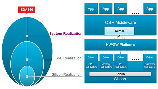
Per JohnB: EDA360is a top down approach starting with System Realization – to SoC Realization – ending with Silicon Realization. The WHY of EDA360makes complete sense, great vision, I’m on board, I even have an EDA360shirt. The question I had was: exactly HOW was this going to work? I still do not know the answer.
My last blog: Cadence EDA360 is Paper! (The one year anniversary is paper by the way, thus the title) was also a positive one:
I think EDA360 is an excellent road map for Cadence. The company seems to have focus and hopefully EDA360 products will continue to be developed and deployed.
Cadence centralized product marketing in support of EDA360with JohnB as its leader. Cadence product marketing is back to decentralized reporting into engineering. Marketing versus engineering driven, I miss JohnB Already! R.I.P EDA360!
Note: you must be logged in to read/write comments.


Chemical Origins of Environmental Modifications to MOR Lithographic Chemistry