 A dedicated schematic migration tool can save weeks of effort and allow companies to explore new foundry opportunities. Unfortunately moving analog and mixed signal design data between foundries and processes is a complex business. While engineers would rather spend their days creating new circuits, many spend time translating existing designs by re-creating their data using components from new process design kits (PDKs).
Translating design data is usually a complex process and endless hours of expensive engineering time are wasted copying schematics, swapping new components for old and modifying parameters to satisfy a new PDK. With the increasing reliance on analog circuits in SoCs and an expanding market in analog IP, engineers need to migrate their schematics quickly to run simulations using models in the new PDK. A business can’t respond to new opportunities if it takes weeks before testing can begin in a new process or foundry.
Though it may first appear relatively simple, migrating schematics is much more involved than it looks. Tools must handle physical differences in component symbols and then deal with the hidden mysteries of parameter interactions and component description format (CDF). What starts out looking like a simple case of swapping a few components ends up becoming more and more complex and it’s little wonder that many designers end up copying their schematics manually.
At IN2FAB, we have spent many years building design migration technology as both a migration service company and an EDA tool vendor. Our OSIRIS schematic migration tools have been developed using hundreds of PDK variants for designs from IDMs and foundries and this has given us a great deal of insight in to the challenges of schematic migration. All of our technology is built on the Cadence platform and runs directly with foundry PDKs.
In an ideal world, symbols for components would all look exactly the same; at least for the common ones. If they were all the same size, drawn with the same origin and with pins in exactly the same place, an engineer would just have to change the name of the component library to be well on the way to getting a new circuit. Even if the component names were different, it would just be a case of writing a mapping script to swap one to the other.

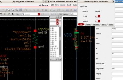
Resistor migrated from source to target processes. Pin names are mapped between the PDKs and a new bulk pin tied to a net, all using the migration tools. Unfortunately, this is rarely the case, especially when moving from one foundry to another. Symbols change size, position and orientation, new pins appear and old ones are removed so swapping one symbol for another just isn’t good enough. Migration tools must take account of physical differences and include an automatic re-wiring capability to reconnect pins that move around or the engineer is left with a circuit full of badly placed components and a string of unconnected wires.
New pins such as bulk connections sometimes appear and they need to be connected while redundant wires that connected old pins that disappeared should be removed. Bulk connections can also be set as a property so this must also be addressed as part of the migration process.
Re-located or new pins can also short with existing wires so a short locator must find and fix places where new pins on bump in to old wires. Even when circuits go between radically different PDKs, they should have clean connectivity after migration without extended manual clean-up.
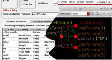
Even when the physical connections are all made, the hidden world of parameters and CDF can present a new round of problems. Entering values for new components using schematic tools is straightforward but mapping properties from one PDK to another is not as easy as it looks. At the simplest level, we need to know the names of the properties on the source and the target symbol and this is usually simple enough to find: e.g. old name = “w”, new name = “width”. With a little trial and error, a mapping system will come together but we also need to get the parameter type to match: e.g. the original is a string: (w = “1u”) while the new one is a floating point number: (w = 1e-06) so this must be adapted by the tools. The callbacks that set other parameters must also be triggered to make sure that everything is set correctly for netlisting and simulation.

These problems become more pronounced when calculating passive values. Migrating the width and length of a resistor is usually pointless as the resistance co-efficient is going to change. Far better to map the resistor value and width and let the new PDK work out what the length should be but that’s going to involve parameter manipulation and callback triggers which are another level of complexity again. A migration tool must analyse the PDKs and present clear information to the user through a GUI; then deal with all of the triggers and callbacks automatically during the migration process.
Lastly, we need to know if our new schematic matches the old one in order to be able to use it for simulation or other work. It’s possible to write netlists for the old and new circuits and run those in to an LVS tool but then we must allow for the differences in component and parameter value names. That can probably be fixed with some sort of perl script but that’s just making our job more complex again. A far better way is using a dedicated schematic comparator that understands all of the mapping and can identify a difference in between source and target in seconds and these are all built in to the schematic migration tools
Larger companies may have a CAD department that will put some sort of customized schematic porting capability in place when they have a big foundry move; doing part of the work and leaving the designers to clean up the rest. If a big corporation is has enough spare time and engineers to dedicate to the problem then they may spare the designers some of the pain but what does a designer do when they want to try out a foundry or two? Or a boutique IP company that’s offering a circuit in a new process they’ve never used before?
The increasing range of foundry and process options along with the dynamic nature of the analog IP market demands that engineers must be able to migrate and test their designs extremely quickly if they are to take advantage of a market window. A fast and intuitive schematic migration capability gives engineers the flexibility to move circuits and simulate in a new process in fraction of the time of other methods.
Tim Reagan
President & CTO at IN2FAB Technology


Musk’s Orbital Compute Vision: TERAFAB and the End of the Terrestrial Data Center