You are currently viewing SemiWiki as a guest which gives you limited access to the site. To view blog comments and experience other SemiWiki features you must be a registered member. Registration is fast, simple, and absolutely free so please,
join our community today!
In the modern electronic world, it’s difficult to imagine any system working as a whole without MEMS (Micro-electromechanical Systems) such as pressure sensors, accelerometers, gyroscopes, microphones etc. working in sync with other ICs. Specifically in AMS (Analog Mixed-Signal) semiconductor designs, there can be significant… Read More
GenApSys is a biotech company developing proprietary DNA sequencing technology. As part of that they develop their own custom sequencing chips. These have an analog component and like many people they use the Cadence Virtuoso analog design environment for this.
I talked to Hamid Rategh who is GenApSys’s VP engineering.… Read More
Custom IC design and layout is becoming more difficult at 20nm and smaller nodes, so the EDA tools have to get smarter and work harder for us in order to maintain productivity with the fewest iterations to reach our specs. Dave Stylesand John Stabenow of Cadence met with me last Monday in Austin at the DAC exhibit area.
John Stabenow… Read More
I’m utterly amazed at how IC-based products are improving our quality of life by implantable devices. The modern day pacemaker has given people added years of life by electrically stimulating the heart. A privately-held company called NeuroPace was founded in Mountain View, California to treat epilepsy by using responsive… Read More
TSMC has been investing in the fabless semiconductor ecosystem for 25+ years and that is why they are the #1 foundry and lead this industry (my opinion). I’m a big fan of joint webinars. Not only is it collaboration open to the masses, it is a close collaboration between the two sponsoring companies. Having worked on the TSMC… Read More
Cadence has brought a suit against Berkeley Design Automation for, as far as I can see, integrating their AFS circuit simulator with the Virtuoso Analog Design Environment (ADE) without using the (licensed) Oasis product. Since BDA is (actually was) a member of the Cadence Connections program, they have to abide by the contract… Read More
In a shocking move TSMC now favors Cadence over Synopsys! Okay, not so shocking, especially after the Synopsys acquisitions of Magma, Ciranova, SpringSoft, and the resulting product consolidations. Not shocking to me at all since my day job is Strategic Foundry Relationships for emerging EDA, IP, and fabless companies.
Rick… Read More
I already talked about how Cadence is splitting Virtuoso into two. Anyway, it is now officially announced. The 6.1 version will continue to be developed as a sort of Virtuoso classic for people doing designs off the bleeding edge that don’t require the new features. And a new Virtuoso 12.1 intended for people doing 20nm and… Read More
Virtuoso Has Twinsby Paul McLellan on 10-18-2012 at 6:01 pmCategories: Cadence, EDA
Cadence has apparently announced that going forward the Virtuoso environment is going to be split into two and offered as two separate code-streams, the current IC6.x and a new IC12.x. The idea is to introduce a new product with features that were specifically developed for new technologies such as double patterning aware layout… Read More
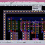
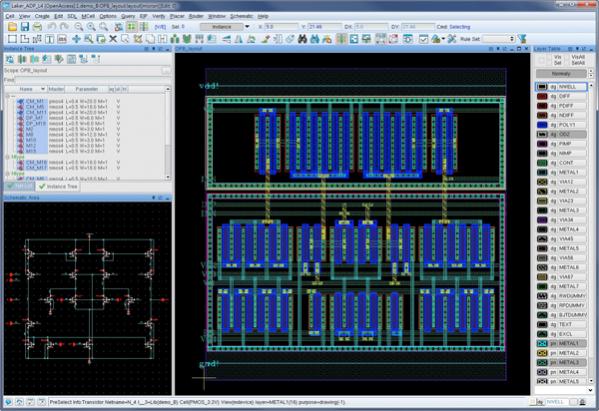
TSMC’s technnology symposium seems to be the new time to make product announcements, with ARM and Atrenta yesterday and Springsoft today.
There is a new incarnation of Springsoft’s Laker layout family, Laker[SUP]3[/SUP] (pronounced three, not cubed). The original version ran on its own proprietary database.… Read More