Usually these brief history pieces are totally written by the SemiWiki blogger whose name is at the top. Often me since that was how I prototyped book chapters (buy). Well, OK, I did actually write this but it is completely cribbed from a presentation earlier this week by Wally Rhines who gave a sort of keynote at the announcement of… Read More

Tag: vhdl
Mark your Date for Semiconductor Design Vision
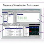
A very popular acronym is ‘WYSIWYG’ – What You See Is What You Get! This is very true and is important to visualize things to make it better in various aspects such as aesthetics, compactness, organization, structure, understandable for correction and so on; the most important, in case of semiconductor design, is being able to identify… Read More
SoC Verification Closure Pushes New Paradigms
In the current decade of SoCs, semiconductor design size and complexity has grown by unprecedented scale in terms of gate density, number of IPs, memory blocks, analog and digital content and so on; and yet expected to increase further by many folds. Given that level of design, it’s imperative that SoC verification challenge has… Read More
Have you Tried ALDEC?
I must admit. I was too comfortable. Let me explain, I’m a ModelSim guy from Mentor Graphics. I did not really think nor care much of the other RTL simulator options. How could someone build a better tool with respect to simulation? Let me introduce you to Aldec. Aldec was founded in 1984 by Dr. Stanley M. Hyduke. 30 years later they are… Read More
Get into a Xilinx FPGA for Under $90
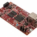
Jump into Xilinx Programmable Logic today! I wanted to encourage my dear readers if you have not tried using an Xilinx FPGA (Field Programmable Gate Array) or even CPLD (Complex Programmable Logic Device) then it is worth your time to begin your evaluation. Maybe you got one for Christmas? If not, it is easier than you think to start… Read More
A Brief History of RTL Design
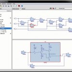
RTL is an acronym for Register Transfer Level and refers to a level of hardware design abstraction using Registers and logic gates. Here’s an example schematic showing one DFF as a register, and one inverter as a logic gate.
Figure 1: RTL diagram of a DFF (D Flip Flop) and Inverter… Read More
How many languages an Engineer should speak?
I speak VHDL and SystemC, others speak Verilog and SystemVerilog … what do you speak?
Before getting into the core of the topic let me give you some round figures, engineers love numbers. Julian Lonsdale “European Sales Manager at Aldec” informed me at the Xfest Munich last month that Aldec carried out a survey to evaluate the usage… Read More
AMS Programmable Prototype Platforms
AVNET released their 15[SUP]th[/SUP] Xfest this year, a couple of months ago. It was here in Germany last week. It was a well organized event, rich with invaluable technical information and full of decent smart engineers and managers. If you missed it this year register for the next event as soon as you can.
It was a very successful… Read More