You are currently viewing SemiWiki as a guest which gives you limited access to the site. To view blog comments and experience other SemiWiki features you must be a registered member. Registration is fast, simple, and absolutely free so please,
join our community today!
This article concludes the three-part series examining key methodologies required for successful multi-die design. The first article Reducing Risk Early: Multi-Die Design Feasibility Exploration focused on feasibility exploration and early architectural validation, while the second article Building the Interconnect… Read More
The semiconductor industry has experienced rapid advancements in recent years, particularly with the increasing demand for high-performance computing, artificial intelligence, and advanced automotive systems. Traditional single-die chip designs are often unable to meet modern PPA requirements. As a result, engineers… Read More
Keysight, with deep roots tracing back to Hewlett-Packard, has long been at the forefront of innovation in electronic design and testing. It manufactures electronics test and measurement equipment and software. The company also owns its own foundry and makes custom chips and packages for its instrumentation business. Many… Read More
At the 2024 TSMC OIP Ecosystem Forum, one of the technical talks by TSMC focused on maximizing 3DIC design productivity and rightfully so. With rapid advancements in semiconductor technology, 3DICs have become the next frontier in improving chip performance, energy efficiency, and density. TSMC’s focus on streamlining the… Read More
Establishing void-free fill of high aspect ratio TSVs, capped by a thin and uniform bulk layer optimized for removal by CMP, means fully optimizing each of a series of critical phases. As we will see in this 3-part series, the conditions governing outcomes for each phase vary greatly, and the complexity of interacting factors means… Read More
Establishing void-free fill of high aspect ratio TSVs, capped by a thin and uniform bulk layer optimized for removal by CMP, means fully optimizing each of a series of critical phases. As we will see in this 3-part series, the conditions governing outcomes for each phase vary greatly, and the complexity of interacting factors means… Read More
Dan is joined by 2023 recipient of the J.J. Ebers award, Dr. Mukta Farooq. This is the highest technical award from the IEEE Electron Devices Society and Mukta is the first woman to earn this prestigious award.
Throughout her career Dr. Farooq has been a trailblazer. She was the first female to earn a Bachelors of Science in Metallurgical… Read More
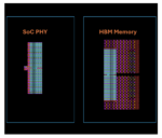
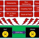
The semiconductor industry has built decades of success on hyper-integration to increase functionality and performance while also reducing system cost. But the standard way to do this, to jam more and more functionality onto a single die, breaks down when some of the functions you want to integrate are built in different processes.… Read More
The old one-size-fits-all approach doesn’t work anymore for DDR4 memory controller IP, especially when addressing the enterprise segments, or application like servers, storage and networking. For mobile or high end consumer segments, we can easily identify two key factors: price (memory amount or controller footprint) … Read More
“Thinking Outside the Chip”by Students@olemiss.edu on 04-13-2016 at 7:00 amCategories: EDA
While pushing Moore’s Law’s boundaries in the world of 2D packaging, companies are starting to explore nontraditional approaches towards designing integrated circuit chips. 2D packaging is currently the most used method in designing chips in the industry, and while it leads in efficiency of power and performance, it lacks … Read More