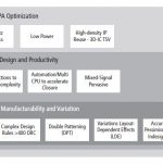
I recently blogged about the actions filed by Tela Innovations at both the US International Trade Commission (USITC) and in federal district court. Those actions allege that five mobile phone manufacturers -HTC, LG, Motorola Mobility, Pantech, and Nokia – were importing handsets into the US which infringed on seven of… Read More
Tag: tsmc
TSMC ♥ Cadence
In a shocking move TSMC now favors Cadence over Synopsys! Okay, not so shocking, especially after the Synopsys acquisitions of Magma, Ciranova, SpringSoft, and the resulting product consolidations. Not shocking to me at all since my day job is Strategic Foundry Relationships for emerging EDA, IP, and fabless companies.
Rick… Read More
Using Soft IP and Not Getting Burned
The most exciting EDA + Semi IP company that I ever worked at was Silicon Compilers in the 1980’s because it allowed you to start with a concept then implement to physical layout using a library of parameterized IP, the big problem was verifying that all of the IP combinations were in fact correct. Speed forward to today and our… Read More
Design IP including Multi-standard SerDes enables risk-free, faster customer ASIC designs
ASIC design service companies are an essential piece of the SC ecosystem, as well as Silicon Foundries, EDA and IP vendors. Their customers range from pure fabless with no ASIC design resources, who need a third party to turn a concept into a real product (IC) and then market and sale it, to large IDM temporarily lacking design resource… Read More
TSMC ♥ Oasys
Oasys has joined the TSMC Soft-IP Alliance Program. This means that TSMC IP partners have access to a new RTL exploration tool to improve QoR and reduce the iterations needed for design closure. In modern process nodes, RTL engineers implementing complex IP cores for graphics, networking, and mobile computing are struggling … Read More
Double Patterning for IC Design, Extraction and Signoff
TSMC and Synopsys hosted a webinar in December on this topic of double patterning and how it impacts the IC extraction flow. The 20nm process node has IC layout geometries so closely spaced that the traditional optical-based lithography cannot be used, instead lower layers like Poly and Metal 1 require a new approach of using two… Read More
Wafer Costs: Out of Control or Not?
I didn’t attend the International Electronic Device Meeting (IEDM) earlier this month, but there have been a lot of reports on the inter webs especially about 20nm and 14nm processes. Some of this is really geeky stuff but I think that perhaps the most interesting thing I’ve read about is summarized in this chart:
This… Read More
Equipment Down 16% in 2012, Flat to Down in 2013
Shipments of semiconductor manufacturing equipment have been trending downward since June 2012, based on combined data from SEMI for North American and European manufacturers and from SEAJ for Japanese manufacturers. The market bounced back strongly in late 2009 and in 2010 after the 2008 downturn to return to the $3 billion… Read More
IP Scoring Using TSMC DFM Kits
Design For Manufacturing (DFM) is the art and science of making an IC design yield better in order to receive a higher ROI. Ian Smith, an AE from Mentor in the Calibre group presented a pertinent webinar, IP Scoring Using TSMC DFM Kits. I’ll provide an overview of what I learned at this webinar.… Read More
Cortex-A9 speed limits and PPA optimization
We know by now that clock speeds aren’t everything when it comes to measuring the goodness of a processor. Performance has direct ties to pipeline and interconnect details, power factors into considerations of usability, and the unspoken terms of yield drive cost.
My curiosity kicked in when I looked at the recent press release… Read More