You are currently viewing SemiWiki as a guest which gives you limited access to the site. To view blog comments and experience other SemiWiki features you must be a registered member. Registration is fast, simple, and absolutely free so please,
join our community today!
Recently, TSMC conducted their annual Open Innovation Platform forum meeting in San Jose. Although TSMC typically eschews a theme for the forum, David Keller, EVT TSMC North America, used a phrase in his opening remarks that served as a foundation for the rest of the meeting – “celebrate the way we collaborate”.
The forum begins… Read More
Last week at TSMC’s OIP symposium, Jen-Tai Hsu, Kilopass’s VP R&D, presented A New Solution to Sensing Scheme Issues Revealed.
See also Jen-Tai Hsu Joins Kilopass and Looks to the Future of Memories
He started with giving some statistics about Kilopass:
- 50+ employees
- 10X growth 2008 to 1015
- over 80 patents (including
…
Read More
This is the 5[SUP]th[/SUP] TSMC Open Innovation Platform Ecosystem Forum and it is not to be missed. Please note that the location has moved from the San Jose Convention Center to the Santa Clara Convention Center which is literally right across the street from the new Levi’s Stadium. If you haven’t been to the new stadium you really… Read More
The success of our semiconductor eco-system depends on collaboration, so the annual TSMC OIP Event just held on September 30 at the San Jose Convention Center was a prime example of that. I didn’t attend this year, but I did follow up with Amit Nandaof Silvaco this week to hear about what they presented. As a consultant I’ve… Read More
TSMC ♥ Cadence!by Daniel Nenni on 10-11-2014 at 4:30 pmCategories: Cadence, EDA, IP, TSMC
One of the questions I routinely ask amongst the fabless semiconductor ecosystem is, “How are the EDA vendors doing?” There are always complaints because, let’s face it, we all like to complain. On occasion however I do hear about a vendor who goes above and beyond the call of duty and it really brightens my day.
Of late,… Read More
Even though the flight to Taiwan is somewhat difficult, I really do enjoy my trips to Hsinchu. In addition to the top two pure-play foundries being there, one of the top SoC companies (MediaTek) and many of the leading semiconductor design companies are there as well. All are a quick taxi ride from my home away from home, the Hotel Royal.… Read More
One of TSMC’s two big Silicon Valley events each year is the Open Innovation Platform (OIP) Forum. This year it is on Tuesday October 1st. It is in the San Jose Convention Center and starts at 9am (registration opens at 8am). Pre-registration to attend is now open here or click on the image to the right.
From 9.10 to 9.40 is the … Read More
The legend of Intel being two process nodes ahead of the rest of the industry is quickly coming to an end. To come to terms with this you need to do an apple to apple comparison which is what I will do right here, right now.
First and foremost let’s compare SoC silicon delivery since SoCs are driving the semiconductor industry and will … Read More
At TSMC’s OIP on October 1st, Mentor Graphics have 5 different presentations. Collect the whole set!
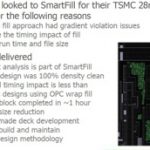
11am, EDA track. Design Reliability with Calibre Smartfill and PERC. Muni Mohan of Broadcom and Jeff Wilson of Mentor. New methodologies were invented for 28nm for smart fill meeting DFM requirements (and at 20nm me may … Read More
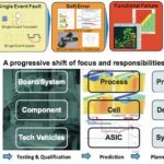
Increasingly, end users in some markets are requiring soft error rate (SER) data. This is a measure of how resistant the design (library, chip, system) is to single event effects (SEE). These manifest themselves as SEU (upset), SET (transient), SEL (latch-up), SEFI (functional interrupt).
There are two main sources that cause… Read More